ISSN(Online) : 2319-8753
I
nternational
J
ournal of
I
nnovative
R
esearch in
S
cience,
E
ngineering and
T
echnology
(An ISO 3297: 2007 Certified Organization)
Vol. 3, Issue 9, September 2014
A Design and Analysis of Low Power Linear
Feedback Shift Register with Clock Gating
P.Mariappan
Professor, Department of ECE, S V College of Engineering, Tirupati, A.P, India
ABSTRACT: This paper presents a method to reduce the power consumption of the popular linear feedback shift register. The proposed scheme is based on the gated clock design approach and it can offer a significant power reduction, depending on technological characteristics of the employed gates. A modified Linear Feedback Shift Register is designed in which power consumption is reduced by deactivating the clock signal to Flip Flop when the output signal is not different from input signal. The power consumption of the new LFSR is reduced due to the reduced switching of Flip Flop To verify, the maximum, minimum and average power of the two LFSRs are the compared.
KEYWORDS: LFSR, PRBGs, Register Transfer Level (RTL), Dynamic Power Management (DPM), Verilog, VHDL.
I. INTRODUCTION
Today, Pseudo-Random Bit Generators (PRBGs) are widely used in many electronic equipment. A good PRBG must be characterized by repeatability (i.e., giving the same output sequence when the same seed is used) and randomness. Today, Hardware implementation of the PRBGs is almost made up of the well-known Linear- Feedback Shift Register(LFSR) whose generic circuit is reported and represented a generic topology of the digital design [1] in Fig.1. This circuit is very simple to be implemented, but since the clock-path of all flip-flops (FFs) toggle at every clock cycle, they consume a significant amount of power.
In this paper, proposed the gated clock design approach for LFSRs[7] which can lead to power reduction without unduly complicating the traditionally simple topology.
In this paper first part will give introduction, 2nd part on clock gating at register transfer level,3rd part gives information about Traditional LFSR, 4th part about gating, 5th part about simulation results, 6th part concludes the paper.
II. CLOCK GATING AT REGISTER TRANSFER LEVEL
Power should be optimized at all stages, but it is generally convenient to address it after Register Transfer Level (RTL).
ISSN(Online) : 2319-8753
I
nternational
J
ournal of
I
nnovative
R
esearch in
S
cience,
E
ngineering and
T
echnology
(An ISO 3297: 2007 Certified Organization)
Vol. 3, Issue 9, September 2014
Fig. 1: A generic topology of the digital design [2]
III. TRADITIONAL LINEAR FEEDBACK SHIFT REGISTER
A linear feedback shift register (LFSR)[6] is a shift register whose input bit is a linear function of its previous state. The only linear functions of single bits are XOR and inverse-XOR[11], thus it is a shift register whose input bit is driven by the exclusive-or (XOR) of some bits of the overall shift register value. As shown in Fig.2, it is obtained with an array of FF’s with a linear feedback performed by several XOR gates. Although LFSR’s are very simple to implement, because they are based on rather complex mathematical theory [8]. However, they can be efficiently describes through the nth order polynomial
Pn(x) = xn + bn-1 xn-1 +bn-2 xn-2 + …….+ b2 x2 + b1 x + 1.
Fig. 2: A Traditional Linear Feedback Shift Register (LFSR). Fig. 4: Gated clock based on synchronization respect to
The bit positions that affect the next states are called the taps. In the diagram below the taps are [16,14,13,11,1]. The rightmost bit of the LFSR is called the output bit and the taps are XOR'd sequentially with the output bit and then fed back into the leftmost bit. The sequence of bits in the rightmost position is called the output stream.
Fig. 3: A 16 bit Linear Feedback Shift Register
ISSN(Online) : 2319-8753
I
nternational
J
ournal of
I
nnovative
R
esearch in
S
cience,
E
ngineering and
T
echnology
(An ISO 3297: 2007 Certified Organization)
Vol. 3, Issue 9, September 2014
The taps of an LFSR can be represented as a polynomial mod 2. This means that the coefficients of the polynomial must be 1's or 0's. This is called the feedback polynomial or characteristic polynomial[3]. For example, if the taps are at the 16th, 14th, 13th and 11th bits (as shown), the feedback polynomial is
x16 + x14 +x13 + x11 + 1.
The 'one' in the polynomial does not correspond to a tap — it corresponds to the input to the first bit (i.e. x0, which is equivalent to 1). The powers of the terms represent the tapped bits, counting from the left. The first and last bits are always connected as an input and tap respectively.
IV. GATING
To reduce the power consumption in a digital system a set of strategies termed Dynamic Power Management (DPM)[4] is often used. The DPMs strategy consists in disabling the logic circuits that are not performing functional operations during a particular time frame, thus reducing power consumption. At circuit level, this strategy is applied by the so
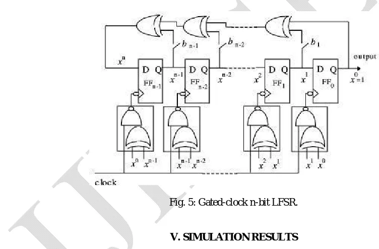
called ―gated clockǁ[11] approach which disables the clock of FFs when output is same as input, as it is shown in Fig. 4 and activating the FF only when the input signal is different from the actual output value. As it can be easily understood, this approach is perfectly compatible with a LFSR only adding some extra gates, as shown in Fig. 5.
Fig. 5: Gated-clock n-bit LFSR.
V. SIMULATION RESULTS
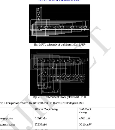
In order to evaluate the power reduction obtained by applying clock gating approach in LFSR, we have evaluated the power consumption in 16 bit Traditional LFSR and power consumption in 16 bit LFSR with clock gating for the same input vector and same clock cycles.
VHDL code of traditional 16-bit LFSR was first simulated in MODELSIM and then Verilog gate netlist was generated by Leonardo, which was then imported in Design Architect which gave the average, maximum and minimum power consumed through ELDO.
ISSN(Online) : 2319-8753
I
nternational
J
ournal of
I
nnovative
R
esearch in
S
cience,
E
ngineering and
T
echnology
(An ISO 3297: 2007 Certified Organization)
Vol. 3, Issue 9, September 2014
Fig. 6: RTL schematic of traditional 16 bit LFSR
Fig. 7: RTL schematic of Clock gated 16 bit LFSR
Table 1: Comparison between 16- bit Traditional LFSR and16 bit clock gate LFSR.
Without Clock Gating With Clock
Gating
Average power 5.6966 Mw 4.913 mW
Maximum power 37.939 mW 30.144 mW
Minimum power 45.6137 nW 62.4403 nW
VI. CONCLUSION
ISSN(Online) : 2319-8753
I
nternational
J
ournal of
I
nnovative
R
esearch in
S
cience,
E
ngineering and
T
echnology
(An ISO 3297: 2007 Certified Organization)
Vol. 3, Issue 9, September 2014
In contrast to the above results, Minimum power was increased by 36%, that may be due to power consumed in initial transitions and that is in order of nano watts, which is too small as compared to power reduction in Maximum power and Average power.
REFERENCES
[1] Qing Wu, Massoud Pedram, and Xunwei Wu, ―Clock-Gating and Its Application to Low Power Design of Sequential Circuits,ǁ IEEE Transactions On Circuits And Systems—I: FundamentalTheory And Applications, Vol. 47, No. 103, March 2000
[2] Walter Aloisi and Rosario Mita, ―Gated clock design of Linear Feedback Shift Registerǁ, IEEE Transactions On Circuits AndSystems—II: Express Briefs, Vol. 55, No. 6, June 2008
[3] L. Lee, S. AI-Sarawi and D. Abbott, ―Low power serial parallel dynamic shift registers,ǁ Electronics letters 9thJnuary 2003 vol.39no.1
[4] Mitch Dale, ―Utilizing clock gating efficiency to reduce power,ǁ EE Times- India January 2008.
[5] Dr. Vishwani Agrawal, “Class slides, Low power design of electronic circuits,” Auburn University, spring 2009.
[6] M. Lowry, “Parallel implementation of linear feedback shift register for low power applications,” IEEE Trans. Circuits Syst.II, Analog Digit. Signal Process., vol. 43, no. 6, Jun. 1996.
[7] M. E. Hamid and C. H. Chen, “A note to low-power linear feedback shift register,” IEEE Trans Circuits Syst. II, AnalogDigit. Signal Process., vol. 45, no. 9, pp. 1304-1307, sep. 1998.
[8] R. S. Katti, X. Ruan, and H. Khattri, “Multiple-Output low-power linean feedback shift register design,” IEEE Trans. Circuits Syst.I, Reg. Papers, vol. 53, no. 7, pp. 1487–1495, Jul. 2006.
[9] T. Lang, E. Musoll, and J. Cortadella, “Individual flip-flops with gated clocks for low power datapaths,” IEEE Trans. CircuitsSyst. II, Analog Digit. Signal Process., vol. 44, no. 6, pp. 507–516, Jun. 1997.
[10] Wonjong Kim, Seungchul Kim, Hanjin Cho, Kwang-youb Lee, “A Fast-Serial Finite Field Multiplier without Increasing theNumber of Registers,” 2003 IEEE, ETRI, Seokyeong University 161, Gajeong-Dong, Yuseong-Gu, Daejeon, 305-350, Korea.