Copyright to IJIRSET www.ijirset.com 9579
Electronic Structure, Electronic Charge Density and
Optical Properties of Organic –Inorganic Hybrid
Semiconductor C
2
H
6
NTeZn
Wilayat Khan
1, Sikander Azam
1, Saleem Ayaz Khan
1, A. H. Reshak
1,21
New Technologies-Research Center, University of West Bohemia, Univerzitni 8, 306 14 Pilsen, Czech Republic
2
Center of Excellence Geopolymer and Green Technology, School of Material Engineering, University Malaysia Perlis,
01007 Kangar, Perlis, Malaysia
*
Corresponding author: Wilayat Khan,
Abstract:
The electronic structure, electronic charge density and optical properties of the organic –inorganic hybridsemiconductor C2H6NTeZn are premeditated by employing the full-potential density-functional technique. The band structure
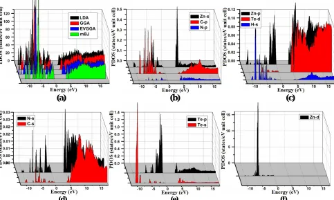
of our optimize crystal indicate semiconductor nature. For understanding the nature of chemical bonding in the investigated material, we calculate the electronic charge density in (110) and (010) crystallographic planes. From the analysis density of states, we emphasize that in the partial density of states, the valence band maximum is contributed strongly from the Zn-d state and a minor contribution from the hybridization of N-s and C-s states. The conduction band minimum is mainly formed from the Zn-s orbital while on the other hand small contribution from Te-p and Te-s states. Further more, we also have calculated the optical properties, to get a physical basis for latent application in optoelectronic devices.
Keyword: Band structure; Density of states; electronic charge density; Optical properties: DFT
I. INTRODUCTION
Crystalline mixtures constructed up of periodically ordered nanostructured inorganic semiconductor motifs and organic molecules are an innovative kind of hybrid semi conducting components that are of large basic significance and technological relevance [1-9]. The mainly interesting characteristic of these components is that many complimentary properties of each individual constituent are conveyed into the hybrid structure by embedding two noticeably different constituents into a single crystal lattice. Integration and blending of outstanding transport properties and structural/thermal firmness from the inorganic constituent and excellent flexibility and possibility from the organic constituent can be anticipated. Moreover, the combining of the inorganic and organic modules in these crystalline hybrid molecules takes location at the atomic level and through chemical bonds, and therefore is free of the interface issues that are unavoidably present in accepted hybrid composite components. In addition, the configuration of such hybrid crystals nearly always leads to exclusive and remarkable new characteristics that are not possible for the one-by-one constituents. Some prominent demonstrations include organic– inorganic perovskite-like structures and associated materials [1-4] hybrid metal oxides [5, 6] and semiconductors created of zinc blende and wurtzite frameworks [7-9]. The II/VI based hybrid semiconductor crystal structures (II: Group 12 components and Mn; VI: Group 16 components) are composed of one-dimensional (1D) chains or two-dimensional (2D) slabs of II/VI semiconductor fragments that are interconnected or divided by organic amine substances to form periodic
crystal lattices. They are of the common equation [MQ(L)x] (M=Mn, Zn, Cd; Q=S, Se, Te; L=organic amine or diamine; and
ISSN: 2319-8753
International Journal of Innovative Research in Science,
Engineering and Technology
(An ISO 3297: 2007 Certified Organization)
Vol. 3, Issue 2, February 2014
Copyright to IJIRSET www.ijirset.com 9580
in the structural, mechanical, and thermal behaviors of these hybrid components. In 2009 Xiaoying Huang et. al. [11]reported
five crystal structures of 3D-[ZnTe(L)0.5] prepared of ZnTe single-atomic slabs and long chain diamines, in addition to their
functional stage transitions, mechanical properties, accurate heat capability, thermal diffusivity, and thermal conductivity. Our analysis displays that crystalline hybrid semiconductors of this kind are much lighter and considerably more bendable than their inorganic corresponding items. The amalgamation of organic substances into the semiconductor crystal lattices also leads to drastically decreased thermal conductivity that is most attractive for high concert thermoelectric materials with functional integrity [12-16].
In this article, we analyze the electronic structure, electronic charge density and optical properties of C2H6NTeZn compound
within the modified Becke and Johnson (mBJ) [17] exchange correlation energy within the framework of full-potential linearized augmented plane wave (FP-LAWP) technique as employed in the WIEN2K package [18].
II. CRYSTAL STRUCTURE AND COMPUTATIONAL DETAIL
For our calculations we use the lattice parameters of the organic –inorganic hybrid semiconductor a-ZnTe(bda)0.5, given in
the crystallographic data (CCDC-736292) [19]. Our investigated compound has monoclinic symmetry with space group
P21/c
, having eight formulas/unit cell. The molecular structure of the investigated compound, is shown in Fig. 1.The full-potential linearized augmented plane wave (FP-LAPW) technique is used to calculate the electronic structure and
linear optical properties of C2H6NTeZn compound, which is based on density functional theory (DFT) as employed in the
WIEN2K package [20]. We carried out the DFT calculations for optimizing the structure of our investigated compound by
minimizing the forces acting on each atom of C2H6NTeZn compound to get stable geometry. The structure of the crystal is
considered to be stable when the convergence of energy criterion 1mRy/a.u. The self consistency is achieved at 10-4Ry. For
our calculations, we choose the RMT values in such a way that no charge leakage is observed from the core and also the
convergence of the total energy was ensured. The Muffin Tin (MT) sphere is expanded up to lmax=10, inside which the
potential and charge density is indicated. We set the value RMTKMAX=7, for the expansion of the basis function.
The electronic exchange-correlation energy is solved by using local density approximation (LDA) [21], generalized gradient approximation (GGA) [22] and Engle Vosko generalized gradient approximation (EV-GGA) [23]. In order to avoid the underestimation of LDA and GGA, we have used the modified Becke-Johnson approximation (mBJ) to get better band gap value. The below equation give mBJ potential and its explanation is found in the Refs [24, 17, 25].
) ( ) ( 2 12 5 1 ) 2 3 ( ) ( ) ( , , r r t c r cv r
v BRX
MBJ X
(1)
Where
N i i 1 2
, represent the electron density,
, 1 * , . ) 2 1 ( i N i i
t
stands for kinetic energy density and MBJ
X
v , stand
Copyright to IJIRSET www.ijirset.com 9581
Fig. 1: Molecular structures of C2H6NTeZn compound
III. RESULTS AND DISCUSSION Electronic structure
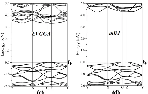
To examine the electronic and optical properties of a compound, it is very useful to investigate the band structure. The band structure has been calculated for the investigated compound using LDA, GGA, EVGGA and mBJ (see Fig. 2).
ISSN: 2319-8753
International Journal of Innovative Research in Science,
Engineering and Technology
(An ISO 3297: 2007 Certified Organization)
Vol. 3, Issue 2, February 2014
Copyright to IJIRSET www.ijirset.com 9582
(c) (d)
Fig. 2Calculated band structures of C2H6NTeZn compound using LDA, GGA, EVGGA and mBJ
Figure 2 (a, b, c and d), shows the band structure of the investigated compound along the selected high-symmetry lines within the first Brillouin zone of the monoclinic crystal. The symbols is assign to high symmetry points of irreducible Brillioun zone (IBZ). Following Fig. 2, it is clear that our investigated compound is a direct band gap semiconductor. From these results, we conclude that mBJ give better band gap value [27-31] as compared to other approximation i.e. LDA, GGA and EVGGA. Due to this reason, mBJ is taken as a best tool for calculating the band gap. The calculated energy band gaps for the four approximations (LDA, GGA, EVGGA and mBJ), are displayed in the Table 1.
Table.1 calculated band gaps of C2H6NTeZn, using LDA, GGA, EVGGA and mBJ
C2H6NTeZn LDA GGA EVGGA mBJ
Eg (eV) 2.79 2.93 3.322 4.25
From the total density of states (TDOS) and partial density of states (PDOS), we can visualize the atomic states hybridization
and contributions to the band in the band structure of C2H6NTeZn compound. Fig. 3(a, b, c, d, e and f), report the calculated
Copyright to IJIRSET www.ijirset.com 9583
(a)
(b)
(c)
(d) (e) (f)
Fig. 3
Calculated total density state (DOS) and partial density of states (PDOS) of C2H6NTeZn compound using mBJElectronic charge density
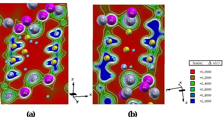
In order to understand the chemical bonding nature of the organic –inorganic hybrid semiconductor C2H6NTeZn, we
ISSN: 2319-8753
International Journal of Innovative Research in Science,
Engineering and Technology
(An ISO 3297: 2007 Certified Organization)
Vol. 3, Issue 2, February 2014
Copyright to IJIRSET www.ijirset.com 9584
(a)
(b)
Fig. 4
Electronic charge density distribution contour calculated with mBJ in the (010) and (010) planes of of C2H6NTeZncompound using mBJ
Optical Properties
The complex dielectric function explains the linear behavior of the system to an electromagnetic radiation. All optical spectra
of C2H6NTeZn organic –inorganic hybrid semiconductor, including real () and imaginary () parts of dielectric tensor,
reflectivity R(), refractive index n(), extension coefficient K(), optical conductivity (), energy loss function L() and
absorption co-efficient I() are calculated and analyzed in detail. The dielectric tensor components for C2H6NTeZn
compound is calculated for both parallel and perpendicular direction of electromagnetic radiation polarization. The momentum matrix elements calculate electron transitions between the occupied and unoccupied states following the selection
rules [32], that result the imaginary part () of dielectric function which is given by ;
n n n n n n c K c K v k c k n v k c k er E E p p dk m e 2 2 2 2 int ) (Im (2)
where p represents the momentum matrix element of the crystals with momentum k.
The symbols cn
k
E and vn
k
E represent the energy for the conduction and valence bands, respectively. The absorption spectrum
is proportional to the total inter-band transitions from the filled valence states cn
k
to vacant conduction states vn
k
over the
K-points of the 1st Brillouin zone. The real part of the dielectric function () is obtained from the imaginary part of the
dielectric function () by using the Kramers–Kronig transformation:
p d
er
0 2 2int 2 Im ( )
) (
Re (3)
The inter-band transition is taken into account during the calculation of the real and imaginary part of the dielectric function
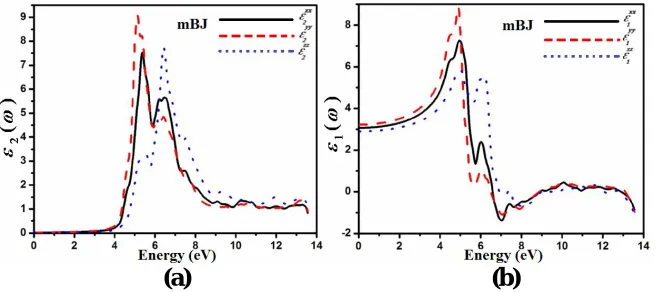
of C2H6NTeZn compound for parallel and perpendicular direction of electric field, is shown in Fig. 5, using mBJ. Our
investigated crystal C2H6NTeZn possess monoclinic symmetry, therefore it contains three nonzero principal dielectric tensor
components of second order, as follow xx(), yy() and zz(). Fig. 5a, shows the plots of 2 () xx ,
) ( 2
yy and
) ( 2
zz ,
which is obtained by using mBJ approximation. The imaginary part () of dielectric function indicates several peaks in the
energy range from 4.6 to 7.0 eV and the main peaks appeared at 5.37 eV for 2xx(), 5.14 eV for ( )
2
yy and 6.4 for ( )
2
Copyright to IJIRSET www.ijirset.com 9585
The real part of the dielectric tensor components 1 ()
xx , ) ( 1
yy , and
) ( 1
zz , as shown in the Fig. 5b. The calculated static
values of the three components 1xx(0)
, 1xx(0)
and 1xx(0)
are 3.07, 3.24 and 2.91, respectively. Our investigated compound
possess a band gap of about 4.26 eV, resulting smaller value of (),which is explained on the basis of Penn model [33].
The Penn model is given by the following relation;
21 ) 0
( Eg
(4)
It is clear from equation (3) that () is inversely proportional to Eg. The compound which has smaller value of band gape
exhibit larger value of ().
(a)
(b)
Fig. 5
Calculated real and imaginary parts of dielectric functions, using mBJBy knowing the real and imaginary part of dielectric function, we can calculate the remaining optical properties like, the
reflectivity R(), optical conductivity (), refractive index n(), extension co-efficient k(), absorption co-efficient I()
and energy loss function L(), respectively.
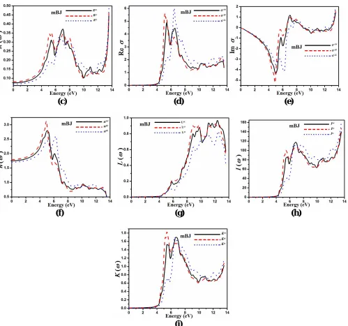
Fig. 5(c), represents the reflectivity spectra Rxx(), Ryy() and Rzz() as a function of energy. The static values of reflectivity
are 4.5 %, 5.0 % and 2.0 % for Rxx(), Ryy() and Rzz(), respectively. For higher energy (13.5 eV), the three components
show maximum reflectivity of 50 %.
The variation in the real Re and imaginary Im part of the optical conduction with photon energy from 0.0 to 13.0 eV,
are shown in Fig. 5(d, e). The optical conductivity () plots indicate big variation at small energy spectrum. The
components of the real part of conductivity i.e. Rexx(), Reyy() and Rezz(), show maximum values around 5.0 eV and
6.0 eV. Two valleys are appeared corresponding to the peaks in the imaginary part of the conductivity at about the same energies (Fig. 5(d, e). It is clear from the Fig. 5(d, e), that the same behavior is observed in both part of conductivity at higher energy along the spectral region.
Fig. 5f, shows the refractive index n() as a function of energy. The static values of the refractive index nxx(), nxx() and
nxx() are found to be 1.73, 1.78, and 1.69, respectively. It is clear from Fig. 5f, that the values of n() increases with energy
in the absorption region, and reaches its maximum value in far ultraviolet region (at about 5.0 eV). At higher energy, beyond 6.0 eV, it tends to decrease and achieve its minimum value at 8.0 eV. One can see from Fig. 5f, that there is a considerable
anisotropy among the three components (nxx(), nxx() and nxx()) of the refractive index.
The extinction coefficient k(), is shown in Fig. 5g. k(), possess maximum peaks in the energy range between 4.8 eV and
7.0 eV. The energy loss function L(), is plotted in Fig. 5h, which exhibits peaks located at energy around 12.6 eV
corresponding to the abrupt decrease in the spectrum of reflectivity R(). The maximum peaks in L() is corresponding to
the screened plasma p [34]. The z-component of the energy loss function shows considerable anisotropy with the other two
ISSN: 2319-8753
International Journal of Innovative Research in Science,
Engineering and Technology
(An ISO 3297: 2007 Certified Organization)
Vol. 3, Issue 2, February 2014
Copyright to IJIRSET www.ijirset.com 9586
the spectral components of absorption co-efficient Ixx() and Iyy() show isotropic behavior and the Izz() shows
considerable anisotropy with Ixx() and Iyy() in the energy range from 5.0 eV to 13.0 eV. One can note that the Ixx()
exhibit maximum value at 7.0 eV and beyond 13.0 eV i.e. at higher energy Izz() indicates higher value as compared to other
two components.
(c)
(d) (e)
(f)
(g) (h)
(i)
Fig. 5
Reflectivity, refractive index, extension co-efficient, absorption coefficient, optical conductivity and energy lossCopyright to IJIRSET www.ijirset.com 9587 IV. CONCLUSION
We studied the electronic structure, electronic charge density and linear optical properties of the organic–inorganic hybrid
semiconductor C2H6NTeZn, using the first principles calculation. Our calculated results for the band structure indicate direct
band gap of about 4.25 eV, using mBJ, which provide better band splitting than the other three approximations. The Te-p, Zn-s and N-p states possess main contribution to the upper part of the valence band, while the lower part of the conduction band is highly contributed by Zn-s orbital with the small support of Te-p and Te-s states. Our calculated electronic charge density repots strong sharing of electrons between C/N with H atoms. We examine that our calculated optical properties show anisotropic nature at the middle of the spectral region. The calculated results of the optical properties show that the
C2H6NTeZn is suitable for optoelectronic devices.
Acknowledgements
This result was developed within the CENTEM project, reg. no. CZ.1.05/2.1.00/03.0088, co-funded by the ERDF as part of the Ministry of Education, Youth and Sports OP RDI program. School of Material Engineering,
REFERENCES
[1] Kagan, C. R., Mitzi, D. B., and Dimitrakopoulos, C. D., "Organic-Inorganic Hybrid Materials as Semiconducting Channels in Thin-Film Field-Effect Transistors", Science, vol. 286, pp. 945-947, 1999.
[2] Mitzi, D. B., "In Progress in Inorganic Chemistry", Vol. 48 (Ed.: K. D. Karlin), Wiley, New York, p. 1, 1999.
[3] Mitzi, D. B., and Kagan, C. R., "In Thin-Film Transistors", (Eds.: C. R. Kagan, P. Andry), Marcel Dekker, New York, pp. 475 2003.
[4] Ishihara, T., "In Optical properties of Low-Dimensional Materials", Vol. 1 (Eds.: T. Ogawa, Y. Kanemitsu), World Scientific, Singapore. pp. 289 – 335 1996.
[5] Johnson, J. W., Jacobson, A. J., Rich, S. M., and Brody, J. F., "New layered compounds with transition-metal oxide layers separated by covalently bound organic ligands. Molybdenum and tungsten trioxide-pyridine", J. Am. Chem. Soc, vol. 103, pp. 5246-5247, 1981.
[6] Yan, B. B., Xu, Y., Goh, N. K., and Chia, L. S., "Hydrothermal synthesis and crystal structures of two novel hybrid open-frameworks and a two-dimensional network based on tungsten(VI) oxides", Chem. Commun, pp.2169-2170, 2000.
[7] Huang, X. Y., Li, J., and Fu, H., "The First Covalent Organic−Inorganic Networks of Hybrid Chalcogenides: Structures That May Lead to a New Type of Quantum Wells", J. Am. Chem. Soc, vol. 122, pp. 8789-8790, 2000.
[8] Huang, X. Y., Heulings, H. R., Le, V., and Li, J., "Inorganic−Organic Hybrid Composites Containing MQ (II−VI) Slabs: A New Class of Nanostructures
with Strong Quantum Confinement and Periodic Arrangement", Chem. Mater, vol. 13, pp. 3754-3759, 2001.
[9] Huang, X. Y., Li, J., Zhang, Y., and Mascarenhas, A., "From 1D Chain to 3D Network: Tuning Hybrid II-VI Nanostructures and Their Optical Properties", J. Am. Chem. Soc, vol. 125, pp. 7049-7055, 2003.
[10] Fu, H., and Li, J., "Density-functional study of organic–inorganic hybrid single crystal ZnSe(C2H8N2)1/2", J. Chem. Phys, vol. 120, pp. 6721 2004. [11] Li, J., et al., "Flexible Hybrid Semiconductors with Low Thermal Conductivity: The Role of Organic Diamines", Angew. Chem. Int. Ed. vol. 48, pp. 7871 –7874 2009.
[12] Fluegel, B., Zhang, Y., Mascarenhas, A., Huang, X. Y., and Li, J., "Electronic properties of hybrid organic–inorganic semiconductors", Phys. Rev. B, vol.70, pp. 205308-12, 2004.
[13] Zhang, Y., Dalpian, G. M., Fluegel, B., Wei, S. H., Mascarenhas, A., Huang, X. Y., Li, J., and Wang, L. W., "Novel Approach to Tuning the Physical Properties of Organic-Inorganic Hybrid Semiconductors", Phys. Rev. Lett, vol. 96, pp. 026405-026409, 2006.
[14] Dresselhaus, M. S., Chen, G., Tang, M. Y., Yang, R. G., Lee, H., Wang, D. Z., Ren, Z. F., Fleurial, J. P., and Gogna, P., "New Directions for Low-Dimensional Thermoelectric Materials", Adv. Mate, vol. 19, pp. 1043-1053 (2007).
[15] Goldsmid, H. J., "Thermoelectric Refrigeration", Plenum, New York, 1964. [16] Rowe, D. M., "Thermoelectrics Handbook: Macro to Nano", CRC, Boca Raton 2005.
[17] Becke A. D., and Johnson, E. R., "A simple effective potential for exchange", J. Chem. Phys, vol. 124, pp. 221101, 2006.
[18] Becke A. D., and Roussel, M. R., "Exchange holes in inhomogeneous systems: A coordinate-space", Phys. Rev. A, vol. 39, pp. 3761-3767, 1989. [19] Li, J., et al., "Angew. Chem. Int. Ed., Flexible Hybrid Semiconductors with Low Thermal Conductivity: The Role of Organic Diamines", vol. 48, pp. 7871 –7874, 2009.
[20] Continenza, A., Wentzcovitch, R. M., and Freeman, A. J., "Theoretical investigation of graphitic BeO", Phys. Rev. B, vol. 41, 3540-3544, 1990. [21] Hohenberg, P., and Kohn, W., "Inhomogeneous Electron Gas", Phys. Rev. B. vol. 136, pp. 864-B871, 1964.
[22] Kohn, W., and Sham, L. J., "Self-Consistent Equations Including Exchange and Correlation Effects", Phys. Rev, vol. 140, A1133–A1138, 1965. [23] Zerarga, F., Bouhemadou, A., Khenata, R., and Bin-Omran, S., "Structural, electronic and optical properties of spinel oxides ZnAl2O4, ZnGa2O4 and
ZnIn2O4", Sol. State. Sci, vol. 13, pp. 1638-1648, 2011.
ISSN: 2319-8753
International Journal of Innovative Research in Science,
Engineering and Technology
(An ISO 3297: 2007 Certified Organization)
Vol. 3, Issue 2, February 2014
Copyright to IJIRSET www.ijirset.com 9588 [26] Blaha, P., et al., WIEN2K: "An Augmented Plane Wave and Local Orbitals Program for Calculating Crystal Properties", edited by K. Schwarz, Vienna University of Technology, Austria 2001.
[27] Tran, F., et al., "Band gap calculations with Becke–Johnson exchange potential", J. Phys. Condens. Matter, vol. 19, pp. 196208- 196216, 2007. [28] Reshak, A. H., and Khan, S. A.,"Electronic structure and optical properties of In2X2O7 (X = Si, Ge, Sn) from direct to indirect gap: An ab initio study",
Computational Materials Science, vol. 78, pp. 91–97, 2013.
[29] Reshak, A. H., Kamarudin, H., Kityk, I. V., and Auluck, S., "Electronic structure, charge density, and chemical bonding properties of C11H8N2Oo
-methoxydicyanovinylbenzene (DIVA) single crystal", journal of material science, vol. 48, pp. 5157-5162, 2013.
[30] Reshak, A. H., Khyzhun, O. Y., Kityk, I. V., Fedorchuk, A. O., Kamarudin, H., Auluck, S., and Parasyuk, O. V., "Electronic Structure of Quaternary Chalcogenide Ag2In2Ge(Si)S6 Single Crystals and the Influence of Replacing Ge by Si: Experimental X-Ray Photoelectron Spectroscopy and X-Ray
Diffraction Studies and Theoretical Calculations", Sci Adv Mater, vol. 5, pp.316-327 -12, 2013.
[31] Reshak, A. H., Kityk, I. V., Parasyuk, O. V., Fedorchuk, A. O., Alahmaed, Z. A., Alzayed, N., Kamarudin, H., and Auluck, S., "X-ray photoelectron spectrum, X-ray diffraction data, and electronic structure of chalcogenide quaternary sulfide Ag2In2GeS6: experiment and theory", journal of material
science, vol. 48, pp. 1342-1350, 2013.
[32] Wooten, F., "Optical Properties of Solids", (New York, Academic Press), 1972.