University of Twente
Faculty of Electrical Engineering,
Mathematics & Computer Science
Design of a fully integrated RF
transceiver using noise modulation
Dlovan Hoshiar Mahrof MSc. Thesis
April 2008
Supervisors: Prof. Dr. Ir. B. Nauta Prof. Dr. Ir. J.C. Haartsen Dr. Ing. E.A.M. Klumperink
Abstract
Preface
In accordance with the degree of Master of Science in Electrical Engineering, I present this thesis entitled “Design of a fully integrated RF transceiver using noise modulation”.
I wish to take this opportunity to thank my advisors Mr. Bram Nauta, Mr. Eric Klumperink and Mr. Jaap Haartsen in giving me this chance to learn from their experiences throughout this project.
I would like also to express appreciation to the entire IC Design group in University of Twente for their support and nice time.
Also I am very grateful to UAF (De Stichting voor Vluchteling-Studenten UAF) for their intensive support and guiding throughout my study and my life.
To the heart who always loves without limit, my dear mother Zakia Al Hawezi.
Contents
Chapter 1 Introduction ... 1
1.1 Background ... 1
1.2 Problem definition ... 2
1.3 Proposal solution ... 3
1.4 Objective ... 4
1.5 Report survey ... 4
Chapter 2 Noise Modulation system ... 5
2.1 Noise modulation concept ... 5
2.2 System description ... 5
2.1.2 Baseband Noise Modulation transceiver ... 6
2.2.2 Passband Noise Modulation transceiver ... 13
2.3 Time analysis ... 15
2.1.3 Channel noise contribution ... 20
2.2.3 Non-Integer ratio of Δω en Rb Frequency offset ... 21
2.4 Frequency synchronization ... 23
Chapter 3 : System Design Optimization ... 25
3.1 Multiplier vs. Mixer ... 25
3.2 Baseband Filter ... 30
3.3 De-Spreading Block ... 32
3.4 Total schematic of the Noise Modulation system ... 34
Chapter 4 Receiver requirements & Optimization ... 35
4.1 System requirements (NF and Gain) ... 35
4.2 Squarer Block ... 37
4.3 Mapping system requirement to block requirements ... 53
Chapter 5 Conclusions ... 59
References: ... 61
Appendixes: ... 63
1. The power spectral density of STx(t) ... 63
2. Simulink Model for the Noise Modulation ... 64
3. Fourier series of a square signal ... 66
4. Bulk effect derivation of the Square component ... 67
5. Taylor expansion of Iout ... 68
6. NF derivation for the Squarer Block ... 69
7. Voltage gain derivation for the Squarer Block ... 71
8. Sensitivity equation vs. Friis NF equation ... 72
9. Second iteration level diagram with LNA ... 74
Chapter 1
Introduction
Recently, a lot of applications require the using of Ad hoc sensor networks, to measure the physical properties of the environment (e.g. temperature, air pressure, humidity ...). In those networks, there are two important challenges regarding the implementation of their transceivers, namely robust communication and low power consumption. The concept of Noise Modulation is explained and motivated to be a potential solution. Building a whole transceiver based on this concept is a big task because it requires deep investigations into a lot of interesting aspects, on the system as well as on the circuit level. Therefore, the focus of this thesis will be presented in the objective section. Finally, the chapter ends with the organization of the thesis.
1.1 Background
Wireless distributed sensor networks consist of a collection of communicating nodes, where each node incorporates:
• One or more sensors
• Processing capability in order to process sensor data and to accomplish local control
• A radio to communicate information to/from neighboring nodes and eventually to external users.
In the recent years, different communication concepts have been developed in sensor ad hoc networks through intensive research. This research has highlighted the relevance of the following specifications:
Cost: Each sensor embraces different complex functions. Those functions must be in coherence with each other so that the total system works properly. Implementing those complex sensors in very large numbers increases the cost. Fortunately, emerging CMOS and MEMS technologies reduce the cost per sensor to adequate prices.
Power consumption: In ad hoc networks, each node has its own digital signal processing capability. Consequently, there are two main contributions to the power per node, digital part (DSP) and the analogue part (Radio).
Theoretically, the attenuation increases at least quadratically with the distance between the transmitter and receiver –node. Therefore, using two hops of length L as shown in Figure 1 is better from the power consumption view of point, than using a single hop with length L. Therefore, the transmitted power can be reduced by using a multi-hop communication scheme.
Performance: The nodes are distributed in a harsh environment, where there are a lot of interfering signals. In such an environment, Spectral Spreading transmission systems can provide more robust communication than the conventional narrow band systems. By spreading the spectrum of an information signal over a much wider band than the information rate, the system provides attractive capabilities, namely, anti-jam capability, interference (multipath path and other interference signals) rejection and a low probability of intercept (LPI) capability. Moreover, spreading allows for multiple user random access communication with selective addressing (e.g. via different code, CDMA). Processing Gain (PG) measures how much spreading has been achieved and is equal to PG = Bss/B, where Bss is the spread spectrum transmitted signal and B is the
bandwidth of the information signal. There are different ways to spread the information signal for example: Direct Sequence (DS), frequency hoping, Time hoping and Hybrid systems (Rappaport [6]).
In recent research, a lot of attention has been spent to reduce the power consumption in the Spectral Spreading systems (special in DS systems), while retaining an adequate performance. To explain why the power consumption is critical in wireless sensor networks, the following example is presented.
A typical battery that is usually used in distributed nodes, for instance Lithium Thiony1 Chloride battery, has a capacity of 2000 mAh and a nominal voltage of 1.2 V. By assuming that the battery lasts between 2 to 4 years per sensor, Table 1 shows the maximum allowable current and power consumption.
Number of years Number of
hours Current consumption [µA] Power consumption [µW]
2 17 520 114 136.8
4 35 040 57 68.4
Table 1: Power and current budget of a typical battery
However, in many application battery replacement is highly undesired and the use of an energy harvesting techniques (e.g. solar cells). For compact systems with an area <1cm2, typical energy harvesting devices produce a power in the range of 1-100 µW (IEEE [7]).
This research aims at the design of a low power transceiver for a power consumption level compatible with energy harvesting or batteries with very long lifetime. The focus is on ad hoc sensor networks in low throughput applications. In those applications, the measured data, like temperature, moisture and gas, does not change fast. Accordingly, the transmitter of the reporting node needs to be ON just for low “duty cycle”, while the receiver of the listening node requires being ON most of the time.
1.2 Problem definition
From one side, the conventional Multiple Access (MA) techniques like FDMA, TDMA and CDMA are not attractive because they require a lot of coordination between the transmitters and the receivers; those techniques are based on an absolute frequency, time and code sequence which must be known in the receiver.
reducing the received SNR. Reducing the SNR makes it difficult to synchronize the reference signal (i.e. the reference code in the DS technique) in the receiver with respect to that in the transmitter. As a consequence, the transmitted power has to be increased. The conventional Spread spectrum systems are not adequate in relation to this issue. Therefore, additional power must be consumed in the synchronization operation to be able to implement MA and to achieve higher processing gain.
1.3 Proposal solution
A particular WB transmission technique, called the Frequency Offset Division Multiple Access (FODMA) has been studied in the Telecommunication Engineering Group at the University of Twente, Shang [1], Balkema[2] and IEEE paper[3]. In FODMA or Noise Modulation as depicted in Figure 2, the reference signal (Xref) is a broadband noise which
is transmitted together with the modulated information data.
Figure 2: Noise Modulation schema
The clean reference signal is separated from the modulated information data by offset frequency ∆ω, so that the cross-correlation between those two signals is equal to zero (in other words: the two signals will not disturb each other). At the receiver, the modulated data and the reference signal are simply correlated to reconstruct the information data without the need to regenerate and synchronous the carrier.
The channel definitions in FODMA are not based on absolute parameters but relative
1.4 Objective
In this Master project, the focus concerns two major points:
1. Investigating the feasibility of an implementation of this transceiver in CMOS. 2. Specifying and designing the critical building blocks with a special emphasis to
low power consumption in the receiver.
1.5 Report survey
Chapter 2
Noise Modulation system
The aim of this chapter is to provide an understanding about the Noise Modulation system. After a short introduction about the concept of Noise Modulation, the chapter begins with the system description, where two types of communication systems are explained, namely the baseband Noise Modulation transceiver and the Passband Noise Modulation transceiver. After that a time analysis about the system operation is presented. This analysis provides a new way to understand the signal processing, the channel noise contribution and the effect of using a non integer ratio between the offset frequency ∆ω and the bit rate, on the bit error rate (BER). Finally, the phase synchronization of the local oscillator in the transmitter to that employed by the receiver has been analyzed to show its influence on the communication performance.
2.1 Noise modulation concept
Shannon’s Channel Capacity theory indicates that the signal energy for communications in the AWGN channel should be allocated equally over all frequencies in the band. The signal that is able to achieve that is a sample function of white noise. In the Noise Modulation system, the reference signal is a broad band noise that approximate the Shannon signal. By spreading the spectrum of an information signal with this reference signal, the modulated information will also become a broadband signal. Therefore, both the reference and the modulated signal approximate the Shannon signal so that by using the Noise Modulation concept, a higher capacity can be obtained in comparison to the other spread spectrum techniques.
2.2 System description
2.1.2
Baseband Noise Modulation transceiver
Figure 3 shows the baseband transceiver model. In this model, the transmitted signal is located in the baseband. The information data m(t) has the form of polar NRZ1.
Figure 3: Baseband Noise Modulation transceiver
The wideband noise reference signal Xref(t) is generated by the transmitter and has a
Gaussian probability density function, with a mean value equal to zero. The power spectral density of the reference signal is:
⎩ ⎨
⎧ − < < =
otherwise B f B l f
X X X
ref
0 )
( Equation 2-1
,with a mean power equal to . The modulation block spreads the power of the information data over the reference signal to construct the Sinfo(t) signal. The basic
principle of the Spreading and De-Spreading operation is explained in
l BX
2
Figure 4. When the modulated data and the reference signal are transmitted over a channel as shown in Figure 4, the original information signal can be reconstructed by the following calculation (Balkema [2]):
( )
t(
m t X( )
t)
X( )
t m t X( )
ty = ( )× ref × ref = ( )× ref2 Equation 2-2
Figure 4: Basic principle behind spreading and de-spreading
By writing Xref(t) as it Fourier series representation, one can see that the signal consists of
a series of cosine waves each with random phase shifts. By taking Xref(t) = cos(ωt) gives:
( )
t m t( )
t m t(
(
t)
y ω 1 cos 2ω
2 ) ( cos
)
( × = × +
= 2 1
)
Equation 2-3
When y(t) is low pass filtered only the desired information data remains.
As mentioned in the previous chapter, in order to send both the modulated data Sinfo(t)
with the reference signal Xref(t) together without interfering each other, those signals have
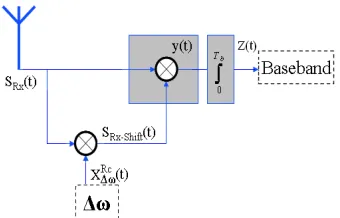
to be separated by offset frequency ∆ω at the transmitter. At the receiver2 the same shift operation is done to retain the information data as shown in Figure 5. The Figure also shows that this frequency shift in the transceiver is implemented by using an oscillator to generate the offset frequency signal X∆ωand a multiplier.
Figure 5: Implementing the offset frequency in the Noise Modulation transceiver
At the transmitter, the Sinfo(t) and the Sref(t) will not interfere with each other, because
their cross-correlation is equal to zero:
( )
cos(
)
then: :assuming
A XΔω t = ωΔωt
(
)
[
( )
(
)
]
[
( )
( )
(
)
]
( )
(
)
(
)
[
]
( )
(
)
[
]
[
(
)
]
0
sin sin
,
0 ref
ref
ref ref
ref Tr
ref info
ref Sinfo
Sref
=
+ Δ ×
+ ×
× =
+ ×
× + Δ × =
+ ×
× ×
= + ×
= +
= Δ
4 4 3 4
4 2 1 ω φ
τ
τ φ
ω
τ τ
τ ω
t E
t X t X E m
t X m t
t X E
t X m t X t X E t
S t S E t
t R
Equation 2-4
Another function for the offset frequency at the transceiver is to implement the Multiple Access by utilizing different frequency. The bandwidth of the reference signal BX is much
larger than the offset frequency and the offset frequency is much larger than the bandwidth of the information data B, hence BX >> ∆ω >> B (later this point will be
explained). The frequency spectrum which has been drawn in Figure 5, is just to show the concept of using the offset frequency. In order to have an advanced picture about the frequency spectrum, the power spectral density expression of STX(t) must be derived and
carefully analyzed. The spectral density is derived from the autocorrelation function. The autocorrelation of STx(t) has been derived in Appendix 1 for Figure 6 (the role of block C
will be explained later) :
( )
τ( )
τ( ) (
τ cos ωτ)
2 1
C2 + Δ
=
ref ref ref
ref Tx
TxS X X X X
S R R
R Equation 2-5
Figure 6: Noise Modulation transceiver
2 After the antenna, there exist a filter with a bandwidth that is just wide enough to accommodate the
Now one can find easily the power spectral density of the STx(t):
Power info ref
)
Equation 2-8
The expression of Equation 2-8 shows that the spectral density of the transmitted signal consists of three broadband signals as shown in Figure 7 (the purpose of drawing those three signals in a stacked blocks above each other is to have a clear view, whereas in the real picture they are overlapping on each other with ∆ω << BX). Thus, the energy of
Xref(t) is divided equally between Sinfo(t) and Sref(t).
Figure 7: Power spectral density of the transmitted signal STx(t)
The last point at the transmitter is to calculate the transmitted bit energy3:
(
)
B lbit time the
Equation 2-9
l
For an ideal channel, the received signal SRx(t) is equal to the transmitted signal STx(t)
with a spectrum shown in Figure 7. The received signal SRx(t) will be shifted by a
frequency , which is equal to under the condition of ideal phase synchronization between the transmitter and the receiver. This shifting operation produces SRx-Shift(t). Then
a linear multiplier correlates between SRx(t) and SRx-Shift(t) to produce two baseband
peaks, one peak exists around zero [Hz] and the other peak exists around 2∆ω [Hz]. Both peaks contain the same information data (i.e. two copies of the same information data). To explain why the de-spreading operation produces those two peaks, let’s go throughout the spectrum at the receiver:
Rc
fΔω fTr ω
Δ
The power spectral density of the signal SRx-Shift(t) is expressed as follows:
)
Equation 2-11
This power spectrum is drawn in Figure 8:
Figure 8: Power spectral density of the signal SRx-Shift(t)
A linear multiplier between SRx(t) and SRx-Shift(t) in time domain translates to a
convolution operation in frequency domain:
(
)
The convolution operation of Equation 2-12 is graphically explained in Figure 9:
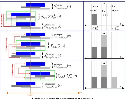
Figure 9: De-spreading operation at the receiver
Thus, the results of the de-spreading process are two peaks. Figure 9 also shows that the offset frequency ∆ω must be larger than the bandwidth of the information data B, so that the two peaks does not interfere each other.
The energy of the peak, which is around the 0 [Hz] is two times the energy of the second peak. By using a low pass filter as shown in Figure 10, the information data will be reconstructed.
In the real world, the channel adds noise. Shang explained how this thermal noise will spread throw the receiver till it reaches the output of the low pass filter. The signal at the output of the low pass filter Z(t) constructs from a baseband polar NRZ E{Z(t)} and a noise nZ(t):
The quantification of the SNR at the output of the low pass filter is necessary to have an intuitive measure for describing the quality of the output signal, and to measure the Bit Error Rate (BER) of the system:
( )
Shang made the derivation of the SNR of Equation 2-14 and found:
PG
Equation 2-15
Since the output signal E{Z(t)} is a baseband polar NRZ signal in Additive White Gaussian Noise (AWGN), and assuming symbols 1 and -1 occur with equal probability, one can find that BER of the FODMA system working in the baseband is (Haykin [4]):
⎟⎟
Where erfc is the complimentary error function:
( )
x( )
y dyEquation 2-16
Differentiating the denominator of Equation 2-15 with respect to C and PG, gives the following two conditions in order to maximize the BER:
77 . 0
= = Coptimum
C Equation 2-17
O b
optimum N
E
Equation 2-19
Then the BER is:
Shang also explained that the communication performance is slightly degraded when the value of C = 1 and keeping the condition of Equation 2-18 to be still satisfied:
1
=
C Equation 2-21
O b optimum
C
N
E
PG
PG
1
.
65
1
=
=
⎯
⎯→
⎯
= Equation 2-22This makes the BER to be:
⎟⎟ ⎠ ⎞ ⎜⎜
⎝ ⎛ =
O b e
N E erfc
P 0.079 2
1 Equation 2-23
Equation 2-18 shows that for a given Eb/NO, the processing gain should be as close to
Goptimum for the low error rate. This means that PG should be adaptively optimized to
different values of Eb/NO Forexample, if 15 dB < Eb/NO < 20 dB, then G = 20 dB should
be the best choice as shown in Figure 11.
2.2.2
Passband Noise Modulation transceiver
In the RF application, the transmitted signal must be shifted to the RF domain as shown in Figure 12.
Figure 12: Passband Noise Modulation transceiver
The Passband transceiver is almost the same as a baseband transceiver, except that both the modulated information data and the reference signal are up-converted to the passband, by a cosine wave with a carrier frequency of ωF, where ωF >> BX >> ∆ω >> B. The
concept of the noise modulation does not change because the same operation is done in the RF domain in stead of the baseband domain.
The output signal E{Z(t)} is again a baseband polar NRZ signal in AWGN, and assuming symbols 1 and -1 occur with equal probability, one can find that BER of the FODMA system working in the baseband is (Haykin [4]):
⎟⎟ ⎠ ⎞ ⎜⎜
⎝ ⎛ =
2 2
1 SNR
erfc
Pe Equation 2-24
Shang made the derivation for the SNR:
( )
{ }
[
]
(
)
(
)
PGC C N
E C C N
E PG C
C C
N E t
Z E SNR
O b
O b
O b nZ
2 2 2 2
2 2 2 2
2 4
2 2
2
2 1 1
1 2
1
5 + + + + ⎟⎟
⎠ ⎞ ⎜⎜ ⎝ ⎛ ⎟⎟ ⎠ ⎞ ⎜⎜
⎝
⎛ + +
⎟⎟ ⎠ ⎞ ⎜⎜ ⎝ ⎛
= =
σ
Equation 2-25
Differentiating the denominator of Equation 2-25 with respect to C and PG, gives the following two conditions in order to maximize the BER:
1
= = Coptimum
C Equation 2-26
O b optimum
N E PG
Then the BER is:
⎟ ⎟ ⎠ ⎞ ⎜
⎜ ⎝ ⎛ =
O b
e N
E erfc
P 0.054
2 1
minimum Equation 2-28
For a fixed bandwidth system with limited output power, the energy per bit can be controlled by changing the processing gain. The performance for various PG is plotted in Figure 13. It can be seen that for lower Eb/NO, a lower PG is better.
Figure 13: Single user performance transmitted in passband when C=1
Finally, by comparing Equation 2-23 with Equation 2-28, one can see that the link performance of the FODMA system in the baseband is better than the Passband. This is because with the same Eb/NO, less power of the transmitted signal for the system working
2.3 Time analysis
Visualizing the system operation in time domain leads to gain deep view into the concept of Noise Modulation. Let’s assume, first that the ratio between the bit rate (Rb4) and the
offset frequency (Rb/∆ω) is an integer for instance, Rb = 1MHz and ∆ω = 2 MHz (Next
section deals with the situation where the ratio of (Rb/∆ω) in not integer) and,
second that the offset frequency signal at the receiver is synchronized to the offset frequency signal at the transmitter.
For the transmitter in Figure 14, the signals are visually analyzed in time
domain. Figure 14: Noise Modulation transmitter
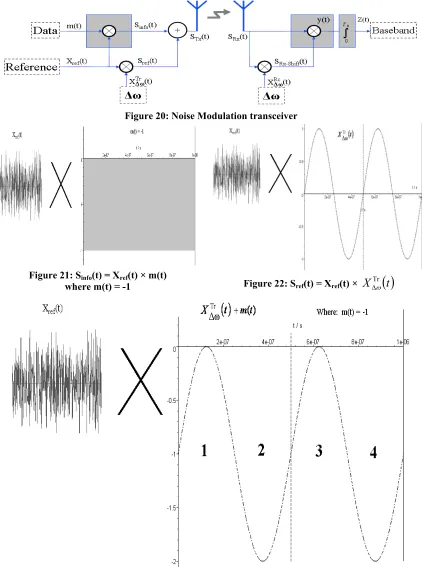
As depicted in Figure 15, Sinfo(t)
contains a Gaussian distributed random part, which is the reference signal Xref(t)
and a deterministic part, which is the bit 1:
( ) ( )
t mt Xt
Sinfo()= ref ×
Figure 15: Sinfo(t) = Xref(t) × m(t) where: m(t) = 1
As depicted in Figure 16, Sref(t) consists
of a Gaussian distributed random part
Xref(t) and a deterministic part, which is
the offset frequencyXTr
( )
t signal: ωΔ
( )
t X( )
t Xt
Sref( ) ref Tr
ω
Δ
× =
Figure 16: Sref(t) = Xref(t) × XΔTrω
( )
tThe transmitted signal STx(t) as shown
in Figure 17 contains a Gaussian distributed random part Xref(t) and a
deterministic part XTr
( )
t + m(t). ωΔ
The deterministic part shapes the random part so that the energy of the random part is distributed around the two peaks of the deterministic part. Thus, there are two active regions inside a bit time namely, the 1st and 3rd
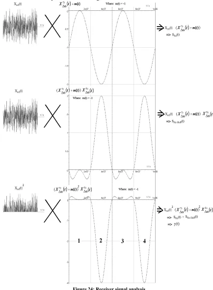
region. Figure 17: STx(t) = Sinfo(t) + Sref(t) where: m(t) = 1
4 R
For an ideal channel (noiseless), the received signal is equal to the transmitted signal. The receiver of Figure 18 multiplies the received signal with the shifted version of the received signal to produce y(t) as shown in Figure 19. The deterministic part of y(t) gathers the energy of the random part in the 1st and 3rd -quarter of the bit time. Thus, the integration operation of the baseband filter is active just in those two regions.
Figure 18: Noise Modulation receiver
The same analysis can be applied when the bit is zero as shown in Figure 21, Figure 22, Figure 23 and Figure 24.
Figure 20: Noise Modulation transceiver
Figure 21: Sinfo(t) = Xref(t) × m(t)
where m(t) = -1 Figure 22: Sref(t) = Xref(t) × XΔTrω
( )
tAs shown in Figure 24, the deterministic part of the signal y(t) gathers the energy of the random part in the 2nd and the 4th -quarter of the bit time. Thus, the integration operation of the filter is active just in those two regions.
In the previous analysis, the role of the XRc
( )
tω
Δ in reconstructing the bit at the receiver is
implicitly presented. To explain this role, let’s write the equation of y(t):
( )
(
( )
)
( )
4 4 4
4 3
4 4 4
4 2
1 3 2
1 DeterministicSignal
Rc 2 Tx
samples positive Random
2 (t) X t m(t) X t
X t
y = ref Δω + × Δω Equation 2-29
The deterministic part contains two Offset frequencies, one is generated at the transmitter and the other is generated at the receiver. Now let’s draw the deterministic part of the signal y(t):
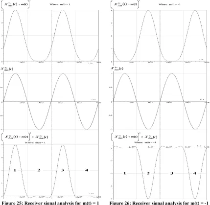
Figure 25: Receiver signal analysis for m(t) = 1 Figure 26: Receiver signal analysis for m(t) = -1
The signal is positive and concentrated in the 1st and 3rd quarter for the situation where Bit 1 is sent, and the 2nd and 4th quarter for the situation where Bit 0 is sent, as shown in
( )
(
2) (t m t XTr +
Δω
)
Figure 25 and Figure 26. The XRc
( )
tω
Δ at the receiver determines if the
signal must stay positive or flip to become negative. This way of analysis is practical to study the influence of the phase synchronization of at the receiver to that at the transmitter.
( )
(
)
2) (t m t +
( )
tω
XTr
Δω
XTr
Δ
( )
t XRcω
2.1.3
Channel noise contribution
In this section, the previous time analysis is extended to include the contribution of the AWGN channel noise. As mentioned before the channel noise process n(t) is modeled as an Additive, White and Gaussian Noise, whose mean power spectral is zero and whose power spectral density is constant. Assuming that there is no attenuation in the channel, the received signal is equal to the transmitted signal plus the channel noise n(t):
( )
(
( )
)
(
( )
)
( )
Equation 2-30
Assuming XRc
( )
t XTr( )
tEquation 2-31
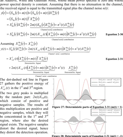
The dot-dashed red line in Figure 27 gathers the positive energy of
in the 1st and 3rd region.
) (
2 t
Xref
The two grey peaks is multiplied by the random part: 2n(t)Xref(t),
which consist of positive and negative samples. The results of this multiplication are positive and negative samples, which they will be concentrated in the 1st and 3rd region, where also the desired signal exists. The negative samples distort the desired signal, hence they distort the detection operation.
Figure 27: Deterministic parts of Equation 2-31 (m(t) = 1)
Figure 28: Deterministic parts of Equation 2-31 (m(t) = -1)
The positive samples of n2(t) are multiplied by two cycles of XRc
( )
tω
Δ , which consist of
two positive and negative peaks. The results are 4 regions, namely two regions of positive samples and two regions of negative samples. The baseband filter will average those samples. If the energy of the channel noise n(t) is low, then the contribution of
can be neglected.
Δ Figure 28 shows the deterministic parts of Equation 2-31
2.2.3
Non-Integer ratio of
Δω
en R
bFrequency offset
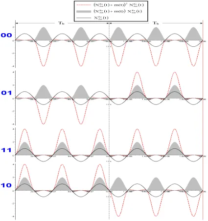
All the explinations and the examples that are till now presented, assume an integer ratio between Δω en Rb5 Carefully inspecting Equation 2-31 and Figure 27, one can recognize
the appearance of an inhomogeneous distribution of the signal and the noise per bit, if the ratio between Δω en Rb becomes non-integer as shown in the example of Figure 29,
where Δω = 2.5 MHz and Rb = 1 M samples/s. In this example, two bit times must be
drawn so that theXRc
( )
t complete its cycle. ωΔ
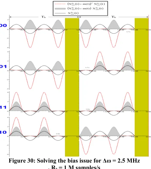
Figure 29: Bias issue for Δω = 2.5 MHz , Rb = 1 M samples/s
This inhomogeneous distribution of the signal and the noise per bit causes different probability in detecting the zero and one -bits in each pattern, namely 00, 01, 11 and 10. Thus, it degrades the performance of the system as it is shown later.
5 R
The distribution can be made homogeneous by letting the filter of Figure 20 to integrate from 0 to 4/5 Tb as shown in Figure 30.
A Simulink model as explained in Appendix 2 for the Noise Modulation system is built to inspect the effect of the bias issue on the BER. The results of our model are shown in Figure 31.
Figure 30: Solving the bias issue for Δω = 2.5 MHz , Rb = 1 M samples/s
As you can observe in Figure 31 that when there exists a non-integer ratio between Δω en Rb (Δω = 2.5 MHz, Rb = 1 M samples/s) then the BER performance degrades, if the filter
integrates over the whole bit time as shown by Curve 2. Using the solution depicted in Figure 30 improves the BER as shown by Curve 3. However even this solution is not enough to improve the BER to that degree shown by Curve 1, where there exist an integer ratio between Δω en Rb (Δω = 2 MHz, Rb = 1 M samples/s). This is because of an
inefficient use of one bit time interval.
Thus, choosing an integer ratio between Δω en Rb provides the maximum performance,
due to the maximum utilizing of one bit time interval.
2.4 Frequency synchronization
In the ideal case, the receiver needs to be coherent in the sense that it requires two forms of synchronization for its operation:
1. Phase synchronization, which ensures that the local oscillator in the receiver is locked in phase with respect to that employed in the transmitter.
2. Timing synchronization, which ensures proper timing of the decision-making operation in the receiver with respect to the sampling instants (i.e. switching between bits 1 and 0)
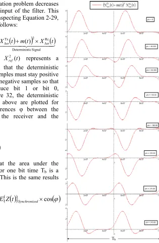
The phase synchronization problem decreases the bit energy at the input of the filter. This can be explained by inspecting Equation 2-29, which is rewritten as follows:
( )
(
144( )
4424)
4443( )
3 2
1 DeterministicSignal
Rc 2 Tx
samples positive Random
2
) ( )
(t X t m t X t X
t
y = ref Δω + × Δω
As mentioned that represents a
positive samples and that the deterministic part decide if those samples must stay positive or convert to become negative samples so that the filter will produce bit 1 or bit 0, respectively. In
) (
2 t
Xref
Figure 32, the deterministic part of the equation above are plotted for different phase differences φ between the local oscillators in the receiver and the transmitter:
( )
t(
t)
XTr sin ω ω = Δ
Δ
( )
(
ω ϕ)
ω = Δ +
Δ t t
XRc sin
Figure 32 shows that the area under the deterministic signal for one bit time Tb is a
cosine function of φ. This is the same results as what Chang found:
( )
{ }
Z t NotSynchronized = E{ }
Z( )
t Synchronized×cos( )
ϕE
Figure 32: Phase synchronization problem
The conventional way to solve the phase synchronization problem is to use the IQ Costas loop as shown in Figure 33 . However, the Costas loop is just able to solve phase differences less than 45o.
Figure 33: Costas loop receiver
Solving the phase synchronization issue in the analogue domain requires extra components to process the received signal. Mostly, the signal processing in digital domain, where flexible and accurate phase correction algorithms can be easily implemented, requires less energy than in analogue domain. Therefore, we suggest solving the synchronization issues in the digital domain as shown in Figure 34, where the IQ structure provides information about the complex plan of the received signal. The Analogue to Digital Converter (ADC) component samples the IQ signal and converter it to the digital domain.
Chapter 3
: System Design Optimization
After understanding the operation and the signal processing of the Noise Modulation system, this chapter optimizes the design choices at the system level. This optimization is necessary to characterize the system components. The chapter begins with studying the possibility of using Switch Mixers instead of Linear Multipliers to reduce the noise figure of the system. The next section is about the optimum design for the baseband filter in order to achieve a maximum BER performance. Then, the de-spreading block will be introduced and a simpler implementation of it will be explained. The chapter ends with the final schematic of the Noise Modulation system.
3.1 Multiplier vs. Mixer
Switch Mixers are preferable to Linear Multipliers because of their higher gain and lower noise contribution. Figure 35 shows four Linear Multipliers of 1, 2, 3 and 4. The aim of this section is to search the possibility to replace Linear Multipliers of 1, 2 and 3 with Switch Mixers. The 4th Multiplier is necessary to be as linear as possible, because it is
responsible about the de-spreading process at the receiver, hence it has a critical influence on the quality of the detection operation.
Figure 35: Noise Modulation transceiver
The linear Multiplier of 1 can easily be replaced by a Switch Mixer, because the data m(t)
is a series of 1 and -1 signals (i.e. a polar NRZ signal). However the replacing of Linear Multipliers of 2 and 3 with Switch Mixers demands that the old X
( )
t ATr( )
tSine
Tr ω
ω = × Δ
Δ sin
and X
( )
t ARc( )
tSine
Rc ω
ω = × Δ
Δ sin
Tr Square
A ARc
must become square signals, with a frequency of ∆ω and amplitude of and Square, respectively as shown in Figure 37 and Figure 39.
Figure 36: Sinfo(t) = Xref(t) × m(t)
where m(t) = -1 Figure 37: Sref(t) = Xref(t) × X
( )
tTr
ω
Figure 36, Figure 37, Figure 38 and Figure 39 present the time analysis.
Figure 38: STx(t) = Sinfo(t) + Sref(t)
Where m(t) = -1
The interesting point appears when comparing regions 1 and 3 in the deterministic part of
y(t) between Figure 24 and Figure 39. Figure 39 shows that the deterministic part of y(t)
is zero in those regions, while Figure 24 shows that the deterministic part of y(t) contains a positive signal in those regions. This positive signal gathers the positive samples of
and produces undesired positive samples (Only the negative samples of y(t) are useful for the detection of bit 0), hence they decrease the energy bit at the output of the baseband filter.
( )
t Xref2Therefore, by using switched mixers, we may expect an improvement of the performance.
As shown in the figures below, the same time analysis has been done when bit 1 is sent. Again one can observe that the whole energy are only concentrated in regions 1 and 3.
Figure 40: Sinfo(t) = Xref(t) × m(t) where m(t) = 1 Figure 41: Sref(t) = Xref(t) × XTr
( )
tω
Δ
Figure 43: Receiver signal analysis
The Simulink model of chapter 2 has been used to measure the BER for this new system, where Linear Multipliers of 1,2, and 3 are replaced by Switch Mixers. The switch Mixer is modeled by using a multiplier and an oscillator that produce a square signal with a frequency of ∆ω and unity amplitude. An ideal square wave does not exist in the reality, therefore a 6 level Fourier series version of the square signal is chosen (See Appendix 3). In order to have a fair BER comparison between this new system and the old one, the amount of power that those Switch Mixers produce must be equal to that produced by Linear Multipliers. This is achieved as follows:
39 . 1 2 2
6
1
2
= ⎟ ⎠ ⎞ ⎜ ⎝ ⎛ × =
=
∑
=
n n Rc
Sine Tr
Sine
B A
A
[ ]
V Equation 3-1where
π
π n
A n
A B
Rc Tr
n
Square Square 4 4
=
= is the amplitude of the nth element of the Fourier series of the square signal, which has an amplitude of Tr = =1
Square
A Rc
Square
To complete the picture, the channel noise contribution must also be included. For this purpose Equation 2-31 has been rewritten below:
( )
Figure 44 plot the deterministic parts of Equation 3-2. The BER performance depends on the SNR at the output of the baseband filter:
1. The signal is represented by the dash-dot red line in Figure 44 and Figure 45. In Figure 44, the area under this line in the 1st and 3rd region are approximately
equal to that of Figure 45, while as mentioned before that regions 2 and 4 in Figure 44 do not have a negative effect on BER in comparison to the signal of the same regions in Figure 45. Thus, the quality of the signal will be improved by using Switch Mixers.
Figure 44: Deterministic parts of
Equation 3-2 when Switch Mixers are used (m(t)=1)
Figure 45: Deterministic parts of Equation 3-2 when Linear Multipliers are used
(m(t)=1)
2. The noise is essentially represented by the grey curve in Figure 44 and Figure 45. The area under the grey curve in the 1st and 3rd region on Figure 44 is approximately equal to that of Figure 45. Interesting point is that the grey curve in the 2nd and 4th region in Figure 44 is zero, while those regions in Figure 45
contribute some noise. Thus, less channel noise contribution exists at y(t) by using Switch Mixers.
Therefore, the SNR will be improved by using Switch Mixers, which means a better BER performance. The Simulink model verifies our expectation as shown in Figure 46.
Figure 46: Comparing the BER performance between using Linear Multipliers or Switch Mixers
3.2 Baseband Filter
This section investigates the optimum design for the baseband filter (See Figure 47) to increase the bit energy with the assumption that the criterion of the phase synchronization is satisfied.
Figure 47: Noise Modulation transceiver, the linear Multiplier are replace by the Switch Mixers
The baseband filter integrates the energy for the duration of one bit time Tb. The result of
the integration is compared to a threshold value so that a decision can made whether bit 1 or 0 has been sent. This block consists of three components:
Integration and Dump (I&D): it creates a cumulative sum of the input signal, while resetting the sum to zero according to a fixed schedule at the end of Tb.
Sample and Hold (S/H): it acquires the output signal of I&D component when it receives a trigger event before the resetting operation of I&D component. Then it holds the output at the acquired input value until the next triggering event occurs.
Comparator: it balances the output of the S/H component to a threshold to make a decision about the transmitted bit.
Figure 48 shows a simple example of this
block, where the working principle is Figure 48: An example of baseband filter uses I&D
presented. The shape of y(t) is approximated by two blocks for each bit as depicted in Figure 49. The scenario of our example assumes that bit 1 and bit 0 have been sent.
Figure 49: Approximate presentation of y(t)
As depicted in Figure 50, the integrated signal of I&D component will be sampled at Tb. The comparator compares the sample
to the threshold signal, which is equal to zero in our system.
The optimum design for the baseband is the Matching6 Filter. The distribution of the
energy for bit 0 is different than that for bit 1 as shown in Figure 49. Consequently, the impulse response of the optimum filter must match the shape of the input signal for bit 1 and bit 0 as depicted in Figure 51. As a result, the matching Filter has an impulse response of a block with unity amplitude and a width of Tb, which is a Sinc function in
Figure 51: Impulse response of the Matching Filter
the frequency domain. The output of the Matching Filter is the convolution between its impulse response hBBF(t) and its input signal y(t) (See Figure 49):
( )
t y( )
ρ h(
t ρ)
dρz = +∞
∫
BBF −∞ −
Equation 3-3
The result of the convolution operation is depicted in Figure 52. The S/H acquires a sample at Tb for each bit. Both bits 1 and
0 will have the same bit energy because the amplitudes of those two samples are equal. By replacing I&D component with the Matching Filter in our Simulink model, the BER performance does not
change as shown in Figure 53. Figure 52: Approximate presentation of z(t), when Matching Filter is used
Figure 53: Comparing BER performances for different baseband Filter implementations
The conclusion is that I&D Filter is in fact the Matching filter for our system and can be replaced by a low pass filter + sampling at the proper times (determination of this proper sampling is done in the digital domain).
6 Matching Filter theory states that in order to optimize the detection operation, the impulse response of the
3.3 De-Spreading Block
The de-spreading block as shown in Figure 54 has the responsibility of de-spreading the received broadband signal at the antenna.
Figure 54: Noise Modulation transceiver
Since multiplication is a commutative operation, the receiver in Figure 54 can be drawn in more convenient form as given in Figure 55 (Massachusetts [5]).
Figure 55: Noise Modulation transceiver
Although that our system uses the mentioned Switch Mixers, but it is interesting to redraw Figure 9 for our new system so that we get an approximate picture about the spectrum of signals p(t) and y(t). This is done in Figure 56.
The spectrum of p(t) will be concentrated at Δω with a bandwidth of B. Multipling p(t)
with , which applies the frequency offset Δω to the receiver, results in the spectrum shown in
( )
t XRcω
Δ
Figure 57, which is exactly equal to the spectrum of y(t) in Figure 9.
Figure 57: Spectrum of y(t)
3.4 Total schematic of the Noise Modulation system
In summary of the system analysis, Figure 58 presents the total schema for the Noise modulation system:
1. At the transmitter, a power amplifier is needed to amplify the power to the required level, which is 0 dBm.
2. At the receiver, a Front End RF Filter is needed to filter the out of band signals as mentioned previously. The bandwidth of this filter is equal to the bandwidth of the broadband signal STX(t),100MHz around 2.4 GHz.
3. Three from four Linear Multipliers can be replaced by Switch Mixers. This improves the NF of the system, which means that there is no need to spend extra power consumption to raise the desired signal above the noise.
4. The de-spreading block can be implemented in a more convenient way by using a square component and a Switch Mixer in place of using a Linear Multiplier and a Switch Mixer.
5. Finally, I&D is the matching filter for our system. It can be replaced by a low pass filter + sampling at the proper times (determination of this proper sampling is done in the digital domain).
Chapter 4
Receiver requirements & Optimization
After optimizing the design choices on the system level, it is the time to map the system requirements to block requirements of the receiver. This is necessary to specify some important requirements for the receiver integration on a chip, and also to estimate the required power consumption. The chapter begins to calculate the required voltage gain and the noise figure (NF) of the receiver. After designing the squarer component, those gain and NF are distributed over receiver’s components. Finally, the chapter ends with a discussion.
4.1 System requirements (NF and Gain)
The fundamental blocks, which are necessary for the signal processing operation in the receiver, are plotted in Figure 59. The Front End components, namely RF Filter, Squarer block, Switch Mixer and the
Baseband filter, needs to amplify the received signal at the antenna to an appropriate level above the noise so that the ADC can process it. Therefore it is necessary to specify the required voltage gain and NF for the receiver.
Figure 59: Noise Modulation transceiver
In our derivations, an ideal case is assumed, where the transmitting and receiving antennas are in a free space without boundaries or obstructions. The received signal power at the antenna is given by Rappaport [6]:
( )
4π
dOLG G P
P T T R
R 2 2
2
λ
= Equation 4-1
This equation is known Fiis Free space equation, where: PT : Transmitted signal power
G : Antenna gain (transmitter and receiver side)
dO : is a distance of 1m between the transmitter and the receiver
L : The system loss
λ : Signal wave length, which is equal to mm
GHz f
c RF 125
4 . 2
10 3 /
8 = ×
= =
λ
For isotropic7 antennas and no system loss, the ratio between transmitted signal power and received signal power is called Path Loss (PL(dO)):
( )
4 ⎟2⎠ ⎞ ⎜
⎝ ⎛ = =
λ
π O
R T O
d P
P d
PL Equation 4-2
By using the Log-distance Path Loss Model [6], Equation 4-2 can be extended to calculate PL for higher distances than just 1m:
( )
⎟⎟ ⎠ ⎞ ⎜⎜ ⎝ ⎛ +
⎟ ⎠ ⎞ ⎜
⎝ ⎛ =
⎟⎟ ⎠ ⎞ ⎜⎜ ⎝ ⎛ +
=
O O
O O
d d n
d
d d n
d PL PL
log 10 4
log 10
log 10
2
λ π
Equation 4-3
where n depends on the specific propagation environment. As an example for an urban area cellar radio n is in the range 2.7 to 3.5. For our calculation n is assumed to equal to
3. In addition to that the chosen distance range (d) will be from 1m to 25m. This range is a good start to investigate the feasibility of designing our receiver in CMOS technology. For this range, PL varies from 40 dB to 82 dB. The desired transmitted signal power is specified by PT = 0 dBm. Thus, the received signal power is in the range -40 dBm (2.22
mV) to -82 dBm (17.8 μV).
From one side, the signal with -40 dBm is the maximum signal that can be expected at the antenna. The Front End amplifies this signal to a level, which is in some radio receivers below the full scale of the ADC with few dB’s. Leaving those dB’s below the full scale can serve as margin for power from other nearby strong signals. However, our system does not need this margin due to that the received signal is a spread8 spectrum signal. Therefore, the Front End amplifies the signal with -40 dBm to the level of the full scale (Vmax) of the ADC. In most typical ADC, the
full scale is around 300 mV. Consequently, the required voltage gain is:
dB V G
dB P
FE
R
5 . 42
10 * 50 * 001 .
0 /10
max
max
= =
Figure 60: Mapping the applied signal level into the AD Converter
From the other hand, the signal with -82 dBm is the minimum signal level that the system can detect with achieving an acceptable signal to noise ratio (SNR) as shown in Figure 60. The acceptable SNR is related to a desired BER. For our system the desired BER must be less or equal than 10-4, which according to Chang [1] the required SNR must be larger or equal to 11.4 dB:
BER ≤ 0-4 → SNR ≥ 11.4 dB.
8 Spread spectrum communication system has a high immunity against the interference signals. This is
y sensitivit R
P specifies the maximum allowed NF for the Front End [8]:
( )
[dB] [dB]log 10 [dbm/Hz] 174
[dBm] B SNRmin
P
NFFE ≤ Rsensitivity + − − Equation 4-4
where:
SNRmin : the minimum signal to noise ratio that achieves the desired BER. In our system,
this SNRmin is equal to 11.4 dB as shown in Figure 60.
With PRsensitivity = -82 dBm, SNRmin=11.4 dB and B=1 MHz, the maximum allowed NF
must be 20.5 dB.
The noise floor of the ADC needs to be below the noise floor of the front-end, so that the ADC noise does not contribute in an observable way to the overall NF of the receiver. As the ADC noise begins to contribute to the floor of the receiver, nonlinearities can adversely impact receiver performance, especially when it comes to signal power estimation. Therefore, the ADC noise floor should be as small as reasonable by tuning its sample frequency and number of needed bits.
Thus, the Front End requirements for the front End are as follows:
GFE = 42.5 dB
NF = 20.5 dB
For achieving the mentioned voltage gain and NF, the receiver architecture needs Low noise amplifiers at the RF side (before the Switch Mixer) and/or amplifier at the Baseband side. However it is not possible to make any decision about the receiver architecture without first investigating the design of the Square block. This is the subject of the next section.
4.2 Squarer Block
As mention previously, the Square component is responsible for the dispreading operation, which makes it to be the core of our receiver. Therefore the main criteria in designing this block must be high performance:
1. High performance: The desired output signal must be a lot larger than the distortion, which is generated by the Squarer block.
2. High conversion gain
3. Low power consumption, as the emphasis inside this project is to design low power receiver using the Noise Modulation concept.
Optimum design choice
Saturation Multiplier
The basic condition for a transistor to operate in the triode region is . The drain current has the following equation:
DS TH
GS V V
V − ≤
(
)
22 GS TH
D V V
I =
β
− Equation 4-5Where
L W COX
n μ
β =
By adding the desired RF signal to the gate voltage:VGS =VG+VRF, the drain current becomes:
(
)
(
)
(
)
(
2)
22 2
2
2 2
2
2 2
2
RF GT
RF GT
RF GT
RF GT
TH RF
G D
V V
V V
V V V V
V V
V I
β
β
β
β
+ +
=
+ +
=
− +
=
Equation 4-6
Where VGT =VG−VTH
Although the drain current contains the squaring term , the circuit still needs to cancel the first two terms from
2 /
2 β
RF
V
Equation 4-6.
Linear (Triode) Multiplier
The basic condition to operate in the triode region is VGS −VTH ≥VDS . The drain current has the following equation:
(
)
⎟⎠ ⎞ ⎜
⎝
⎛ − −
= 2
2 1
DS DS
TH GS
D V V V V
I
β
Equation 4-7By makingVDS =VRF, the drain current becomes:
(
)
(
)
22
2 2 1
RF RF
TH GS
RF RF
TH GS D
V V
V V
V V
V V I
β
β
β
− −
=
⎟ ⎠ ⎞ ⎜
⎝
⎛ − −
=
Equation 4-8
The drain current contains the desired squarer term , but again the circuit still needs to cancel the first two terms from
2 /
2 β
RF
V
Subthreshold Multiplier
A transistor operates in Subthreshold region hasVGS ≈VTH . The drain current has the following equation:
T GS
V V O
D I e
I = ζ Equation 4-9
Where ζ >1 is a nonlinearity factor and VT = kT/q = 25 mV
By makingVGS =VG+VRF, the drain current becomes:
T RF T
RF
O T G T
RF G
V V O V
V I
V V O V
V V O
D I e I e e I e
I ζ ζ ζ " ζ
"
= =
=
+
3 2
1 Equation 4-10
Taking the Taylor expansion for around x = 0: ex
... !
2 ! 1
1+ + 2 +
= x x
ex Equation 4-11
for Equation 4-10 gives:
...
2 2 1
0 + + +
= a aV a VRF
ID RF Equation 4-12
As it can be observed that the drain current contains the desired square element 2 ,
2VRF
a
where
( )
2 "2
1 2 VT I a O
ζ
=
In this situation, the circuit needs to cancel a lot of elements from Equation 4-12 that distorts the desired output signal.
The optimum selection between those three choices will be based on our criteria:
1. The performance of the 1st and the 2nd choice are better than the 3rd choice, because their drain current contains less distortion terms. The distortion terms in Equation 4-6 and Equation 4-8 are additive, hence it is easier to cancel them in comparison to those in Equation 4-12, because of the exponential character of Equation 4-10.
2. All the three choices can have higher conversion gain, for example by increasing the width of the transistor.
3. The 2nd choice consumes no DC current in compare to the 1st one. Consequently, the 2nd choice satisfies all our targets as summarized in Table 2:
Saturation Linear Subthreshold
Unwanted distortion terms
Good Good Bad
Power consumption Bad Good Medium
Conversion gain Good Good Good
Component Design
Although the previous section proposes the triode operation region as the optimum choice for building the Square component, there are still terms that must be canceled from Equation 4-8. Figure 61 shows the implementation of Equation 4-8 on a circuit level. The 2.4 GHz RF voltage signal is supplied to terminals (a) and (b) of the MOSFET
Figure 61: Begin concept to build the Square component
transistor. The source terminal alternates between terminals (b) and (a) as the input voltage signal alternates between positive and negative, respectively:
Source
To cancel the RF current from Equation 4-13, the differential structure is used as it is depicted in Figure 62, where VRF =VRF1−VRF2. The terminals (b1) and (a2) are the source terminal for the top and bottom transistor, respectively.
Figure 62: Canceling the nonlinear terms in the output of the Square component
The equation of the top transistor is:
2
The equation of the bottom transistor is:
(
)
Equation 4-15
As VS2 =VRF2then:
Equation 4-16
Finally:Iout =Iin1−Iin2
Equation 4-18
The previous derivations show that the squarer circuit redrawn in Figure 63 produces partly symmetrical terms which stay inside the loop of the Square component, while the asymmetrical current terms flow outside the loop from the output terminal to the negative RF-input.
Till now the operation of the Square component has been analyzed for the first section of the RF signal period. For the second section, similar analysis can be derived to proof the
Figure 64: The current flow for the second section of the RF signal period
results shown in Figure 64. Consequently, in each section of the RF signal period, only one transistor will provide the desired current to the output terminal. In addition, this same transistor that provides the desired current will also generate an extra current due to the bulk effect. This extra current belongs to the group of asymmetrical currents. Therefore it flows towards the output. Fortunately, it is much smaller than the desired square current:
(
)
(
)
⎟⎟⎠ ⎞ ⎜⎜
⎝
⎛ Φ + Φ
= F F
RF
V 2 4 2
8 1 distortion current
effect Bulk
current
Square 3
1 γ
Equation 4-19
Where: ⎟⎟
⎠ ⎞ ⎜⎜ ⎝ ⎛ =
Φ
i sub F
n N q kT
ln [V]
Nsub :Doppingconcentration of thesubstrate γ : body effect coefficient [ V ]
Equation 4-19 has been derived in Appendix 4. For example a 0.5 µm transistor has
V and :
9 . 0
2ΦF =
( )
1/2V 45 . 0
=
γ
VRF1 = 5 mV then 3.76 103
distortion current
effect Bulk
current
Square = ×
The differential input voltage VRF1 and VRF2 is actually the balance side of a BalUn
(BalUn with a centre tap) or the output terminal of a LNA ( in case, the receiver needs the utility of a LNA). In either situation, both VRF1 and VRF2 will have their own internal
impedance. For simplicity, let’s assume that they are two resistances R1 and R2 as shown
Figure 65: Square component
in Figure 65. The existence of those internal resistances complicates the analysis of the output current. For the first section of the RF signal period as shown in Figure 65:
(
)
Solving this equation with respect to Iin1 results in:
But VS2 =−VDS2
Solving this equation with respect to Iin2 results in:
(
)
Finally, the output current becomes:
( ) output current is:
1
The same analysis and results hold for the second section of the RF signal period. Maple9 program has been used to compute the limiting value of Iout as RS approaches zero:
( )
21 0
lim RS→ Iout = −
β
VRF Equation 4-23As expected that the result is equal to Equation 4-18. Although this may be an indication that Equation 4-22 is correct, but it is difficult to recognize how the output current is still a square function of VRF1. Taking the Taylor expansion for the square roots in Equation
4-22 shows the following result (See Appendix 5 for the derivation):
(
1)
3 RF2 1Comparing Equation 4-24 to Equation 4-18, shows that the existence of RS will reduce
the output current of the Square component by factor of
(
1+βRSVGT)
3. In fact, the existence of RS will also bring VGT to the picture, where small VGT increases thetransconductance. To plot this equation, let’s take the following example:
(
2)
, where 2.4GHz sin10 5 V
V, 1 V , 35
mA/V 3 . 38 m
0.35 L and m 75 W
A/V 178.65 C
with m 0.35 : Transistor
3 -RF1
G
2 2 OX
n
= ×
=
= Ω =
= ⇒ =
=
=
RF RF
S
f t
f R
π
β μ μ
μ μ
μ
The output current is plotted in Figure 66. Obviously, the shown output current is a square function of the input signal:
(
)
(
)
(
A t)
A(
(
t)
t A
RF RF
RF
ω
ω
)
ω
2 cos 1 2 sin
I
sin signal
age Input volt
2 2
out ∝ = −
⇒
=
The peak value of the output current is 289 nA.
Figure 66: The output current of the Square component (Theory)
Cadence/SpectraRF has been used to verify our theory, where Model 11 of a 0.35 µm transistor with a gate oxide thickness equal to 6.5 nm have been used to build the Square component. The same values of the previous example have been used in our simulation circuit. The simulation results are depicted in Figure 67. As you can observe that the peak value of the output current is 321.64 nA, which is almost equal to our theory result.
Figure 67: The output current of the Square component (Cadence simulation)
The simulation plot shows a high performance with respect to unwanted spectral components of the Squarer. To check this point in an accurate way, the Discreet Fourier Transform (DFT) of the output current has been plotted in Figure 68. It shows that the
Figure 68: The frequency spectrum of the output current (Cadence simulation)
Hence, the Square component achieves a high performance and consumes almost zero power. Actually, there is a very small DC leakage current that is supplied from VG. The
leakage current crosses the gate oxide and flows towards the drain and the source of the transistors. This current limits the sensitivity of our component to process small input signals and its value depends on the gate oxide thickness and the gate-voltage. Hence, increasing the gate oxide thickness will increase the sensitivity. In the simulation of our previous example (gate oxide thickness is equal to 6.5 nm), the smallest input signal is around 100 pV that the Square component can still process without having distortions from this leakage current. The simulation also shows that decreasing the thickness to 2 nm will reduce the sensitivity to 500 µV and the leakage current is around 200 pA (Cadence simulation).
Optimum W to Maximizing the output current
Let’s now investigate the optimum transistor’s width (W) to maximize the output current for a specific RS value, hence maximizing the conversion gain. Optimizing the
transistor’s width is the same as optimizing β, because β is a function of W
(β=μnCOXW/L). The optimization procedure begins with differentiating the output
current (see Equation 4-24) with respect to β and equating the result to zero:
0
=
β d dIout