Universiteit Twente
Bachelor thesis
Monolayer MoS
2
on a substrate of
hexagonal boron nitride
Author:
Ruben Jaarsma
Period:
2-3-2014 - 4-24-2014
Supervisor:
Nirmal Ganguli
Chair:
Computational Materials Science
Abstract
In this research we want to see if hexagonal boron nitride is a suitable candidate as a substrate for a monolayer of molybdenum disulfide. For a monolayer of molybdenum disulfide on top of a monolayer of hexagonal boron nitride we calculate two possible optimized structures with a distance between the planes of 4.89 ˚A with a binding energy per molybdenum disulfide unit cell of −2.778 eV and 8.10 ˚A with a binding energy per molybdenum disulfide unit cell of −2.634 eV. We plot the total energy versus the seperation distance en find that the structure with a seperation of 4.89 ˚A is a stable structure and the structure with the seperation of 8.10 ˚A is a metastable structure.
We plot the band structure for the metastable structure and find a direct band gap of 1.83 eV at K point. For the band structure of the stable structure we find that the band gap is indirect between H and K. We find that this is because of the bands with nitrogen pz character that have moved down due to hybridization to create an indirect band gap. We plot the projected density of states for the boron nitride atoms and the molybdenum disulfide atoms for the stable structure and find a band gap of 1.83 eV.
Contents
Introduction 3
Background . . . 3
Problem . . . 3
Plan of action . . . 4
Theoretical aspects 5 Tight binding method . . . 5
Density functional theory . . . 6
Structure . . . 7
Binding . . . 8
Computational aspects 9 VASP . . . 9
Density of states . . . 10
Band structure . . . 10
Results 11 Discussion 16 Conclusion 17 Possibilities for future research . . . 17
Appendix 1 - Assignments 21 Assignment 1 - Radial Schr¨odinger Equation . . . 21
Assignment 2 - Tight binding . . . 24
Assignment 3 - Densities of States . . . 36
Assignment 4 . . . 41
Assignment 5 - Tight Binding Method . . . 44
Assignment 6 . . . 55
Appendix 2 - VASP-calculations 57 Carbon . . . 57
Silicon . . . 61
Germanium . . . 61
Boron nitride . . . 62
Aluminium phosphide . . . 67
Gallium arsenide . . . 69
Zinc selenide . . . 69
Introduction
Background
Technology is getting smaller and more compact. Therefore, scientists are always looking for stable materials of very small size with interesting properties. In recent history there has been a lot of talk and research about graphene, a monolayer of graphite. This two-dimensional material has very interesting properties, namely a high carrier mobility and mechanical strength [1]. But it’s not a semiconductor.
After scientists were able to create graphene in the laboratory one knew that is was possible to extract a monolayer of a material. The search for more of these materials continued. A semiconductor material would be especially interesting.
Molybdenum disulfide might be a good candidate for this. A monolayer of molybdenum disul-fide has a direct band gap of 1.8 eV [2], which makes it suitable for opto-electronic applications. If one is to create a monolayer of this material however, a substrate is needed to support this monolayer. Hexagonal boron nitride is used as a substrate for graphene. They have the same honeycomb structure and their in-plane lattice parameters are very similar.
Molybdenum disulfide also has the same honeycomb structure as graphene [3], however it’s in-plane lattice parameter is significantly larger than that of boron nitride. Therefore one may wonder if boron nitride is a good candidate for a substrate. If it is questions arise about how this would effect the direct band gap in monolayer molybdenum disulfide, since bulk molybdenum disulfide has an indirect band gap [2].
Problem
In this thesis we investigate if hexagonal boron nitride is a suitable candidate as a substrate for a monolayer of molybdenum disulfide. This will be done by answering the following three more specific questions:
Are there one or more stable heterostructures of molybdenum disulfide on boron nitride?
Does the direct band gap of monolayer molybdenum disulfide remain direct upon forma-tion of the heterostructure and what is the size of it?
Plan of action
To be able to do this research as a third year bachelor student a lot of preperation had to be done. First an understanding of the electronic structure of solids via tight binding approximation had to be achieved. Several assignments related to tight binding were done of which the results can be found in appendix 1. The chapter Theory has a section dedicated to this subject explaining tight binding and the conclusions that were made from those exercises. These conclusions will be used in analyzing and discussing the results in the chapters Results and Discussion.
Besides the above the program VASP [4] [5] had to be learned. VASP is software used to calculate the electronic properties of materials. To get a good understanding of the software and learn how to extract useful information a lot of calculations were done with group IV, III-V and II-VI semiconductors as well as with carbon. Information about the software VASP is given in the chapter Computational aspects.
The results and an analysis of these VASP calculations can be found in appendix 2. The results were used to discuss the trends found in this region of the periodic table. For example, the band gap size of carbon, silicon and germanium was compared to their lattice constant, as well for germanium, gallium arsenide and zinc selenide. Furthermore, of materials that exist in different structures the most stable structure was calculated based on the total energy per atom.
Theoretical aspects
Tight binding method
The tight binding method is a way of describing solid materials and from there calculate the electronic properties of this material. In tight binding, the solid is seen as “a collection of weakly interacting neutral atoms” where “the overlap of the wave functions is enough to require corrections to the picture of isolated atoms, but not so much as to render the atomic description completely irrelevant.” [6]
For this thesis, the focus will be on the results and interpretation of the tight binding method. Using this model, the Schr¨odinger equation can be rewritten to become
(ε(k)−Em)bm =−(ε(k)−Em) X
n
(X
R6=0 Z
ψm∗(r)ψn(r−R)eik·Rdr)bn
+X
n (
Z
ψm∗(r)∆U(r)ψn(r)dr)bn+ X
n
(X
R6=0 Z
ψm∗(r)∆U(r)ψn(r−R)eik·Rdr)bn (1)
[6]
In this equation ε(k) is the energy dispersion with k the position in k-space in m−1. E
m is the atomic energy. Both the energy dispersion and atomic energy have SI units of joule but it’s in some situations convenient to work with the unit of eV. The indices m and n indicate the atomic orbitals and b is a unit vector. R and r describe the positions of the atoms and are given in meters. The wave function is represented by ψ in units of m−3N/2 in three dimensions with N the total number of atoms and the potential by U, which should be given in the same units as the energy dispersion and atomic energy.
Equation (1) can be used to calculate the energies of different atomic orbitals. For a (non-degenerate) s-level equation (1) will become one single equation. For (triply degenerate) p-levels it will become a 3×3 secular problem and so on.
The tight binding method is of course an approximation, but it’s a good method for simple systems. In appendix 1, several assignments were done using the tight binding method, that is assignments 2, 4, 5 & 6. An insight about the electronic structure of solids was gained from these assignments that can be used in analyzing the results of this research.
Input data
(atom coordinates and number of electrons) Theory level specified
Generate input guess density
Construct the Hartree potential
Construct the effective potential (sum of Hartree, exchange and external potentials)
Solve Kohn−Sham equations
Generate the output density from the solutions to the Kohn−Sham equations
Are the input and output
densities matching?
Output: Calculate energy and
forces Repeat the cycle
using the output density as the input density
YES NO
Figure 1: Flow chart visualizing density functional theory.
In assignments 4 & 5 the tight binding method is used to calculate the p-bands. Calculating these requires exploiting all the symmetries in the system and can only be done analytically for special k-points. In assignment 6, the π (pz) bands of graphene were calculated using thight binding. A comparison between figure 33 and figures 38 and 39shows how accurate the tight binding method can be.
Density functional theory
Density functional theory (DFT) can be best explained in the words of Walter Kohn, developer of DFT:
DFT is an alternative approach to the theory of electronic structure, in which the electron density distribution n(r), rather than the many electron wave function plays a central role. [7]
DFT works in the following steps: guess an electron density, construct the different potentials, solve the Kohn-Sham equations, generate the output density and see if it matches the input density. This is visualized in the flow chart in figure 1.
(a) Top down and side view of a monolayer of hexagonal boron nitride. The boron atoms are shown in green and the nitrogen atoms are shown in grey.
(b) Top down and side view of a monolayer of molybdenum disulfide. The molybdenum atoms are shown in purple and the sulfur atoms are shown in yellow.
Figure 2: Structures of boron nitride and molybdenum disulfide. Images were made using VESTA [11].
Figure 3: Supercell of a 4×4 monolayer of molybdenum disulfide on top of a 5×5 monolayer of boron nitride. The image was made using VESTA [11].
Structure
A monolayer of hexagonal boron nitride has a well known structure, which is shown in figure2a. It has a honeycomb lattice where for each atom the three nearest neighbors are of the different atomic species. [9] The in-plane lattice constant aBN is 2.50 ˚A[10].
Molybdenum disulfide also has a hexagonal honeycomb structure. However a monolayer of molybdenum disulfide actually exists of two layers of sulfur atoms with one layer of molybdenum atoms in between. In figure2ba top down and side view of molybdenum disulfide can be seen. The distance between the sulfur atoms is 3.1 ˚A. The in-plane lattice parameter aM oS2 is 3.12 ˚
A. [3]
Binding
If binding between the layer of boron nitride and molybdenum disulfide will be achieved can be determined in a few ways. First of all one can calculate if the total energy is at a minimum. A second way is to calculate the binding energy. This binding energy is the total energy of the heterostructure minus the total energy of isolated molybdenum disulfide, that is the supercell of the heterostructure without the boron nitride layer, and minus the total energy of isolated boron nitride, the supercell without the layer of molybdenum disulfide. This can therefore be calculated using the following equation:
Eb =Etothet −EtotM oS2 −EtotBN (2)
Computational aspects
VASP
VASP, short for Vienna ab-initio simulation package, is software used for density functional calculations. In this thesis it is used for three things: calculating the optimal structure, the electronic ground state and the band structure of a material. For all of the calculations it needs at least the input files containing the structure of the material, the potential, the k-points that need to be sampled and a file containing different parameters specifying the details of the calculation.
Self consistent calculation This calculation is used to calculate the electronic ground state. The structure of a material should be used as input along with the other mandatory input files. VASP then calculates the electronic ground state properties of the material sampling the whole first Brillouin zone. The output contains but is not limited to the charge densities, the density of states and the energy eigenvalues.
Relaxation This technique is used to calculate the optimal structure. An educated guess of the structure is used as input. Then a self consistent calculation is done. VASP then varies the positions of the atoms and does another self consistent calculation, trying to minimize the force. Once a predefined threshold is reached the output contains the optimal structure.
Band structure calculation To calculate the band structure along a predefined path, the file containing the k-points has to list all of these k-points explicitly. Contrary to the self consistent calculation VASP then calculates the energy eigenvalues only at these k-points instead of the whole first Brillouin zone. To speed up the calculation the charge densities from the self consistent calculation should be used as input so that VASP can use these in it’s calculations. The output contains the energy eigenvalues that can be used to plot the band structure.
Figure 4: First Brillouin zone of a hexagonal lattice, showing the high symmetry points. [12]
Density of states
From the VASP output files the density of states can be determined. It can be used to easily see the band gap and show band widths. From the VASP output files also the projected density of states can be determined. The projected density of states shows the density of states for certain atoms, for example for one species of atoms. This is used in this research to see which bands are boron nitride bands, which are molybdenum disulfide bands and which are hybridized bands.
Band structure
Results
The heterostructure described in the section Structure of the chapter Theoretical aspects has first been relaxed. Two guesses were made for the distance between the planes, namely 5.0 ˚A and 8.0 ˚A, so for the supercell we have c= 10.0 ˚A and c= 16.0 ˚A respectively. From there the relaxations were started and two different optimized structures were found of which the distance between the planes is shown in table 1.
A check was done to see if both structures are stable. For different values of c a self consistent calculation was done, from which the total energy was plotted. In figure 5 the total energy versus the distance between the planes is plotted. The highest total energy was set to zero, with the rest of the values in reference to this. In this figure one can see that there is actually just one stable structure, the one with a distance between the planes of 4.89 ˚A.
The other structure might be metastable. To check that the binding energies were calculated using equation (2). In table1the binding energies for the two solutions are shown. One can see that there is binding for both of the structures, although the structure with a distance of 4.89 ˚
A between the planes has stronger binding. Therefore we conclude that the structure with a distance between the planes of 8.10 ˚A is a metastable structure.
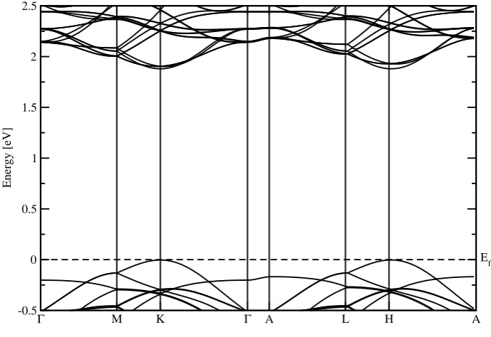
Band structure calculations were done for the metastable structure. The results of these cal-culations are plotted in figure 6. In this figure also the character of the bands was plotted. All graphs have a different character of the bands plotted. The first one shows the molybdenum disulfide dxy bands in red. The second one shows the molybdenum disulfide dx2−y2 bands in magenta. The third one shows the nitrogen pz bands in green. The Fermi level was set to zero in this figure, and is marked by the dotted line.
In this figure, one can see there is an direct band gap at K point where the top of the valence band is a band with nitrogen pz character. The size of the band gap, extracted from this figure, is 1.83 eV.
Band structure calculations were also done for the stable structure, shown in figure 7. This figure also shows the character of the bands in three different graphs, again with the first one showing the molybdenum disulfide dxy bands in red, the second one showing the molybdenum disulfide dx2−y2 bands in magenta and the third one showing the nitrogen pz bands in green. In this figure the Fermi level was again set to zero and marked by the dotted line.
Table 1: Distance between the planes and binding energy per molybdenum disulfide unit cell for two optimal structures found with the relaxation. There is stronger binding for the structure with a distance of 4.89 ˚A between the planes.
Distance between the planes [˚A] Binding energy per MoS2 unit cell [eV]
4.89 -2.778
4 5 6 7 8 9 −16
−14 −12 −10 −8 −6 −4 −2 0
Distance between the planes [Å]
Total energy [eV]
Figure 5: Total energy versus the distance between the planes. The highest total energy was set to zero and the rest of the values are in reference to this zero. The two structures that were found with the relaxation are marked by red circles. One can see that there is actually just one stable structure. The other structure might be metastable.
Figure 7: Region around the band gap for the heterostructure with a distance between the planes of 4.89 ˚A. The character of the bands is shown in the different graphs. The first one contains the molybdenum disulfide dxy bands in red. The second one contains the molybdenum disulfide dx2−y2 bands in magenta. The third one contains the nitrogen pz bands in green.
Figure 8: Band structure in the energy range around the band gap for the stable heterostructure. The Fermi level is set to zero and marked by a dotted line. The bands marked in red are the bands that are not visible in the band structure of isolated molybdenum disulfide.
One can see in figure 7 that the direct band gap has become an indirect gap between H and K. The band with pz character that was at the top of the valence band for the metastable structure has actually shifted down a lot. The top of the valence band now consists of bands with a lot of molybdenum disulfide d character.
Γ M K Γ A L H A -0.5
0 0.5 1 1.5 2 2.5
Energy [eV]
Ef
Figure 9: Band structure in the energy range around the band gap for isolated molybdenum disulfide from the stable structure. The Fermi level is set to zero and marked by a dotted line.
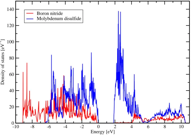
To visualize the hybridization the projected density of states for the boron nitride bands and the molybdenum disulfide bands was calculated for the stable structure. The projected density of states is plotted in figure 10. This figure shows that the top of the valence band consists of hybridized boron nitride - molybdenum disulfide bands.
-10 -8 -6 -4 -2 0 2 4 6 8 10 Energy [eV]
0 20 40 60 80 100 120 140
Density of states [eV
-1 ]
Boron nitride Molybdenum disulfide
Discussion
A stable structure with a distance between the planes of 4.89 ˚A was found. A stable structure was expected, since there was nothing suggesting there wouldn’t be one. The strain is 0.16%, and both materials have a hexagonal structure. Also a metastable structure with a distance between the planes of 8.10 ˚A was found.
Comparing figures 6 and 7 one can notice that the band gap changes from an indirect to a direct band gap if the distance between the layers is increased. This is probably because when the distances between two layers is increased, there is less overlap between the wave functions of these layers. Therefore, there is less hybridization and the band with nitrogen pz character makes up the top of the valence band.
This can also be seen in figures 8 and 9. The top valence band at K-point in isolated molyb-denum disulfide is still the top valence band at K-point in the heterostructure, however it’s not the general top of the valence band anymore. It has probably shifted a little because of hybridization due to the layer of boron nitride in between.
In figure10one can also see that the top of the valence band consists of hybridized molybdenum disulfide and boron nitride bands, although the number of molybdenum disulfide states is higher. Since the band gap of boron nitride is bigger then that of molybdenum disulfide [13] [2] one would expect the bottom of the conduction band to be just molybdenum disulfide bands, as is the case in figure 10.
Also, the change in the band gap from direct to indirect for the metastable structure to the stable structure cannot be due to the molybdenum disulfide layers interacting as in the bulk matrial. Bulk molybdenum disulfide has the top of the valence band at gamma which is clearly not the case in figure 8. [14]
Along the path Γ-A the bands move up in energy as can be seen in figure 8. The difference in energy between Γ and A gets smaller for bands that are higher in energy. This can be explained by looking at the extent of the wave functions. Wave functions for bands with a higher energy have a smaller barrier to the vacuum level. Therefore these wave functions have a larger extent and the slope of the energy band is smaller.
Conclusion
The main question posed in the introduction was if hexagonal boron nitride is a suitable can-didate as a substrate for a monolayer of molybdenum disulfide. We found first of all that there is one stable structure consisting of a monolayer of hexagonal boron nitride and a monolayer of molybdenum disulfide, with a distance between the planes of 4.89 ˚A. We also found a metastable structure with a distance between the planes of 8.10 ˚A.
We found that the direct band gap of a monolayer of molybdenum disulfide does not stay direct for the stable structure. The top of the valence band in isolated molybdenum disulfide moves down a little so an indirect band gap is created between the high symmetry points H and K. This was explained as an effect of hybridization.
From the projected density of states we know that the size of the band gap is 1.83 eV, which matches the size of the band gap for a monolayer of molybdenum disulfide. We know the band gap for the metastable structure, which is also 1.83 eV, from the band structure calculation.
In the heterostructure we saw bands with nitrogen pz character which weren’t visible in the band structure of isolated molybdenum disulfide. We found that for the structure with a distance between the planes of 8.10 eV this band moves up to create a direct band gap at the high symmetry K point.
We can conclude that hexagonal boron nitride in fact is a suitable candidate as a substrate for a monolayer of molybdenum disulfide. However, for a monolayer of molybdenum disulfide on top of a monolayer of hexagonal boron nitride the band gap becomes indirect for the stable structure. It does stay direct for the metastable structure.
Possibilities for future research
In the future tight binding calculations can be done for the hybridization of p and d orbitals from K to H to get more insight as to why the bands shift and the band gap becomes indirect between H and K.
One of the possibilities may be to see what happens if there are more layers of boron nitride. This might lead to the formation of a stable structure with a direct band gap, which is interesting for opto-electronic applications.
Bibliography
[1] A. K. Geim,Graphene: Status and Prospects, Science324, 1530 (2009).
[2] K. F. Mak, C. Lee, J. Hone, J. Shan, and T. F. Heinz, Atomically Thin MoS2: A New Direct-Gap Semiconductor,Physical Review Letters 105, 136805 (2010).
[3] T. Cao, G. Wang, W. Han, H. Ye, C. Zhu, J. Shi, Q. Niu, P. Tan, E. Wang, B. Liu, and J. Feng, Valley-selective circular dichroism of monolayer molybdenum disulphide, Nature communications3, 887 (2012).
[4] G. Kresse and J. Hafner,Ab initio molecular dynamics for liquid metals, Physical Review B 47, 558 (1993).
[5] G. Kresse and J. Furthm¨uller, Efficient iterative schemes for ab initio total-energy calcu-lations using a plane-wave basis set, Physical Review B 54, 11169 (1996).
[6] N. W. Ashcroft and N. D. Mermin, Solid State Physics, college ed. (Thomson Learn-ing, Inc., Berkshire House, 168-173 High Holborn, London WC1 V7AA, United Kingdom, 1976).
[7] W. Kohn, “Electronic structure of matter - wave functions and density function-als,” http://www.nobelprize.org/nobel_prizes/chemistry/laureates/1998/
kohn-lecture.pdf (1999), Nobel Lecture.
[8] J. Hafner, “Foundations of density functional theory,” https://www.vasp.at/
vasp-workshop/slides/dft_introd.pdf.
[9] N. D. Drummond, V. Z´olyomi, and V. I. Fal’ko, “Electronic structure of two-dimensional crystals of hexagonal boron nitride,” http://www.tcm.phy.cam.ac.uk/~mdt26/tti_
talks/qmcitaa_13/drummond_tti2013.pdf (2013).
[10] S. Majety, J. Li, X. K. Cao, R. Dahal, J. Y. Lin, and H. X. Jiang, Metal-semiconductor-metal neutron detectors based on hexagonal boron nitride epitaxial layers,Proc. SPIE8507, 85070R (2012).
[11] K. Momma and F. Izumi, VESTA 3 for three-dimensional visualization of crystal, volu-metric and morphology data, Journal of Applied Crystallography 44, 1272 (2011).
[12] “Brillouin zone of the hexagonal lattice,” http://www.ioffe.ru/SVA/NSM/Semicond/
Append/figs/fmd21_5.gif.
[13] M. Bernardi, M. Palummo, and J. C. Grossman,Optoelectronic Properties in Monolayers of Hybridized Graphene and Hexagonal Boron Nitride,Physical Review Letters108, 226805 (2012).
[14] E. Cappelluti, R. Rold´an, J. A. Silva-Guill´en, P. Ordej´on, and F. Guinea, Tight-binding model and direct-gap/indirect-gap transistion in single-layer and multilayer MoS2,Physical
[15] D. J. Griffiths, Introduction to Quantum Mechanics, second international ed. (Pearson Education, Inc., Upper Saddle River, NJ 07458, USA, 2005).
[16] “P-orbitals,” http://www.sparknotes.com/chemistry/fundamentals/
atomicstructure/section1.rhtml.
[17] D. Gl¨otzel, B. Segall, and O. Andersen,Self-consistent electronic structure of Si, Ge and diamond by the LMTO-ASA method, Solid State Communications 36, 403 (1980).
[18] Wide Bandgap Semiconductors: Pursuing the Promise, Tech. Rep. (U.S. Department of Energy, 2013).
[19] K. Kobayashi, “Graphite band structure,”http://www.bandstructure.jp/Table/BAND/
Graph.html ().
[20] D. D. L. Chung, Review Graphite,Journal of Materials Science 37, 1475 (2002).
[21] C. Kittel, Introduction to Solid State Physics, eighth ed. (John Wiley & Sons, Inc, 111 River Street, Hoboken, NJ 07030-5774, 2005).
[22] N. A. Abdulkareem and B. H. Elias, First Principle Band Structure Calculations of Zinc-Blende BN and GaN Compounds, International Journal of Scientific & Engineering Re-search 4 (2013).
[23] R. M. Chrenko, Ultraviolet and infrared spectra of cubic boron nitride, Solid State Com-munications 14, 511 (1974).
[24] K. Kobayashi, “wBN band structure,” http://www.bandstructure.jp/Table/BAND/
band_png/wBN.png ().
[25] Y.-N. Xu and W. Y. Ching, Calculation of ground-state and optical properties of boron nitrides in the hexagonal, cubic, and wurtzite structures, Physical Review B 44, 7787 (1991).
[26] K. Kobayashi, “hBN band structure,” http://www.bandstructure.jp/Table/BAND/
band_png/hBN_bh_P_0G.png ().
[27] X. Blase, A. Rubio, S. G. Louie, and M. L. Cohen, Quasiparticle band structure of bulk hexagonal boron nitride and related systems, Physical Review B 51, 6868 (1995).
[28] A. Saliev, “Electronic properties of aluminium phosphide,”http://www.institute.loni. org/lasigma/reu/documents/presentations2013/IsaacSaliev_FinalPresentation. pdf (2013).
[29] R. Ahmed, Fazal-e-Aleem, S. J. Hashemifar, and H. Akbarzadeh, First-principles study of the structural and electronic properties of III-phosphides,Physica B: Condensed Matter 403, 1876 (2008).
[30] A. J. Danner, “An introduction to the empirical pseudopotential mehtod,” http://www.
ece.nus.edu.sg/stfpage/eleadj/pseudopotential.htm (2011).
[31] J. E. Bernard and A. Zunger, Electronic structure of ZnS, ZnSe, ZnTe, and their pseu-dobinary alloys, Physical Review B 36, 3199 (1987).
Appendix 1 - Assignments
Assignment 1 - Radial Schr¨
odinger Equation
For this assignment, the radial Schr¨odinger Equation will be solved numerically for a Coulomb potential. The energies of the bound states (1s, 2s, 3s; 2p, 3p) of hydrogen will be found, as well as the corresponding eigenfunctions.
The differential equation for the radial wave function is:
d2u
dρ2 = [1−
ρ0
ρ +
l(l+ 1)
ρ2 ]u=f(ρ)u (3)
[15]
with ρ≡κr,ρ0 ≡ me 2
2π0¯h2κ and κ≡
√
−2mE
¯
h .
Because the equation is solved numerically, the following formula was used:
ui+1 = 2ui−ui−1+f(ρ)ui(∆ρ)2 (4)
The strategy is to integrate the radial equation outwards from the origin and inwards from∞. For the outwards integration the asymptotic form for ρ→0 was used:
u(ρ)∼Cρl+1 (5)
[15]
Then equation (4) was used to calcualate the rest of the terms.
For the inwards integration the asymptotic form for ρ→ ∞ was used:
u(ρ)∼Ae−ρ (6)
[15]
The two wavefunctions were matched at a turning point. In this case the point where the energy is equal to the potential energy was chosen, so that is:
E =− e
2
4π0 1
r =− e2 4π0
κ ρtp
→ρtp =−
e2κ 4π0E
(7)
0 200 400 600 800 1000 −0.08
−0.06 −0.04 −0.02 0 0.02 0.04 0.06
ρ
u(
ρ
)
Figure 11: Example of a kink at the point where the wavefunctions were matched. The kink is marked in red. The solution was found for l = 0 andn = 3.
The principal quantum numbern was determined by counting the number of nodes, that is the number of crossings of the x-axis, using #nodes =n−l−1⇒n = #nodes+l+ 1.
One starts with choosing an energy E, an angular momentum l and a principal quantum number. Then, after calculating what the principal quantum number of the found solution is, change the energy until the correct solution is found.
The found solution still contains a kink, that is a point wich isn’t differentiable, at the turning point where the wavefunctions were matched. An example of such a kink can be seen in figure11. At the point marked in figure 11 the wavefunction is continuous but not differentiable. The solution for the eigenenergy won’t contain a kink. Therefore, the kink should be reduced by making small changes in the eigenenergies. This way the eigenenergy can be found. The found solution still contains a kink, that is a point wich isn’t differentiable, at the turning point where the wavefunctions were matched. An example of such a kink can be seen in figure 11. At the point marked in figure 11 the wavefunction is continuous but not differentiable. The solution for the eigenenergy won’t contain a kink. Therefore, the kink should be reduced by making small changes in the eigenenergies. This way the eigenenergy can be found. The found solution still contains a kink, that is a point wich isn’t differentiable, at the turning point where the wavefunctions were matched. An example of such a kink can be seen in figure11. At the point marked in figure 11 the wavefunction is continuous but not differentiable. The solution for the eigenenergy won’t contain a kink. Therefore, the kink should be reduced by making small changes in the eigenenergies. This way the eigenenergy can be found.
However, this program is not the best at finding the exact energies for the bound states. The program will scan a whole energy range looking for only one solution. Then it repeats itself with a smaller energy step value until the desired accuracy of the solution is reached. Finding the eigenenergies with high accuracy takes too long.
To solve the problems mentioned above a different program was made wich calculates the energies where the kink is zero. It determines the size of the kink for different energies and then interpolates to find the energy where there is no kink. This can be seen in figure12, where plots of the energy vs. the size of the kink are shown. In these plots, every x-axis crossing is an eigenenergy.
Increasing Esteps and thus decreasing the step size of the energy did not yield better results. Therefore, ∆ρ and N had to be adjusted. N should be chosen large enough get the necessary range of ρ. However, a smaller ∆ρ did also not yield better results.
A different option was changing the turning point. The definition of the turning point was changed to be N/2. With this turning point, the energies E1s =−13.5975 eV, E2s =−3.3525 eV,E3s=−1.3725 eV,E2p =−3.3825 eV, E3p =−1.4025 eV were found. These were the best results acquired.
Assignment 2 - Tight binding
This section contains the solutions to the tight binding assignments from the Theoretical Solid State Physics course.
1. Linear H3
(a) The value of β is not the same for all three atoms, since the atom in the middle has two atoms around it.
(b) Considering that the atom in the middle has two atoms around it we have:
hψ H ψi=|a1|2(ε−β)−a∗1a2t−a∗2a1t+|a2|2(ε−2β)−a∗2a3t−a∗3a2t+|a3|2(ε−β)
hψ H ψi=|a1|2ε0−a∗1a2t−a∗2a1t+|a2|2ε00−a∗2a3t−a∗3a2t+|a3|2ε0
(9)
with ε0 =ε−β and ε00 =ε−2β
The equation to solve therefore becomes:
ε0−E −t 0
−t ε00−E −t
0 −t ε0−E
= 0 (10)
Finding a solutions gives us:
(ε0−E)[(ε00−E)(ε0−E)−t2]−t2(ε0−E) = 0 (ε0 −E)[(ε00−E)(ε0−E)−2t2] = 0
E =ε0∨(ε00−E)(ε0−E)−2t2 = 0
E =ε0∨E2−(ε0+ε00)E+ε0ε00−2t2 = 0
E =ε0∨E = 1 2(ε
0
+ε00)± 1
2 p
(ε0−ε00)2−4(ε0ε00−2t2)
(11)
Finding a solution for the energy is a lot harder but in this case still doable. One can imagine that calculating the wave functions would be even harder. Simplifying the algebra by taking β
(a) Sketch of the wave function from equation (22).
(b) Sketch of the wave function from equation (24).
(c) Sketch of the wave function from equation (26).
(d) Sketch of the wave function from equation (28).
Figure 16
We neglectα, we only consider nearest neighbors and we takeβ = 0. This means equation (29) becomes:
ε(k) =εs− X
n.n.
γ(R)eik·R (30)
For an infinite chain of hydrogen atoms, the nearest neighbors are the atoms at positions ±a, so we can calculate
ε(k) = εs−t(eika+e−ika) =εs−2tcos(ka) (31)
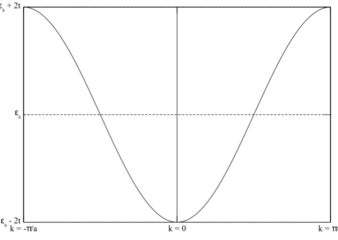
The result is sketched in figure 17from k=−π
a to k= π a.
(b) The Fermi energy is the energy level to which the band is filled. We have a half filled band, so the Fermi energy would be the energy at kf with kf = 2aπ . This means thatεf =ε(2aπ) =εs. The level εs is marked in figure 17. Since the band is only half filled, the electrons are able to conduct so the chain is conducting.
(c) We start at the equation from the slides:
[ε(k)−Em]bm =−[ε(k)−Em] X
n X
R6=0
ψm(r)ψn(r−R)eik·R
bn
+X
n
hψm ∆U(r) ψnibn+ X
n X
R6=0
ψm(r) ∆U(r) ψn(r−R)eik·R
bn
(32)
Again, α is neglected and β = 0. Equation (32) can now be written as:
[ε(k)−Em]bm = X
n X
R6=0
ψm(r) ∆U(r) ψn(r−R)eik·R
bn (33)
k = -π/a k = 0 k = π/a
ε
s- 2t
ε s ε
s+ 2t
Figure 17: Dispersion of an infinite chain of hydrogen atoms.
ε(k)−Es,1 0
0 ε(k)−Es,2
b1
b2
=
P
R6=0hφs,1(r) ∆U(r) φs,1(r−R)ieik·R
P
R6=0hφs,1(r) ∆U(r) φs,2(r−R)ieik·R
P
R6=0hφs,2(r) ∆U(r) φs,1(r−R)ieik·R
P
R6=0hφs,2(r) ∆U(r) φs,2(r−R)ieik·R
b1 b2
(34)
Because we consider s-orbitals, which are always real, one can argue that
hφs,1(r) ∆U(r) φs,2(r−R)i=hφs,2(r) ∆U(r) φs,1(r −R)i=−γ (35)
and, since we have two atoms in the unit cell,
hφs,1(r) ∆U(r) φs,1(r−R)i=hφs,2(r) ∆U(r) φs,2(r−R)i= 0 (36)
and lastly we takeEs,1 =Es,2 =E, so equation (34) becomes:
ε(k)−E 0 0 ε(k)−E
b1
b2
=
0 −P
R6=0γe ik·R
−P
R6=0γeik
·R 0
b1
b2
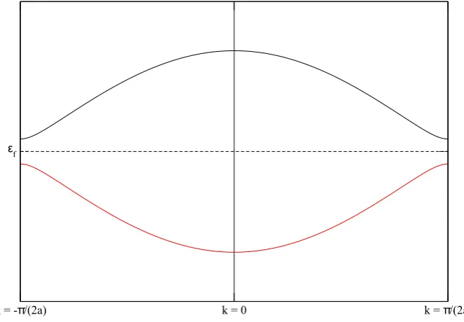
k = -π/(2a) k = 0 k = π/(2a) E - 2t
ε
f
E + 2t
Figure 18: Dispersion of an infinite chain of hydrogen atoms with two atoms per unit cell. The values of k cover the first Brillouin zone. The Fermi energy is marked by a dotted line. The red line represents the solution ε(k) = E+ 2tcos(ka) while the black line represents the solution
ε(k) =E−2tcos(ka).
The energy ε(k) can be found by solving:
ε(k)−E P
R6=0γeik
·R
P R6=0γe
ik·R ε(k)−E
= 0
ε(k)−E t(eika+e−ika)
t(eika+e−ika) ε(k)−E
= 0
ε(k)−E 2tcos(ka) 2tcos(ka) ε(k)−E
= 0
(ε(k)−E)2−4t2cos2(ka) = 0
(ε(k)−E)2 = 4t2cos2(ka)
ε(k)−E =±2tcos(ka)
ε(k) = E±2tcos(ka)
(38)
The dispersion found in equation (38) is plotted in figure 18. In this figure, the Fermi energy is marked by a dotted line. The whole first Brillouin zone is shown.
k = -π/(2a) k = 0 k = π/(2a) ε
f
Figure 20: Dispersion of an infinite dimer chain with s-orbitals. The values of k cover the first Brillouin zone. The Fermi energy is marked by a dotted line. The red line represents the solution ε(k) = E0 − 12
p
∆2+ 16t2cos2(ka) while the black line represents the solution
ε(k) =E0+ 12 p
∆2 + 16t2cos2(ka)
making use of the fact that Es,±=E0± ∆2.
The calculated dispersion is plotted in figure 20. In this figure, the Fermi energy is marked by a dotted line. The whole first Brillouin zone is shown.
(g) The most important difference between dispersion relations calculated in other problems and the one in figure 20 is the band gap. The size of the band gap determines if it’s a semi-conductor or an insulator and thus if conduction is possible. The size of the band gap is equal to ∆, so if the material conducts depens on ∆.
Assignment 3 - Densities of States
Three methods (one analytical, two numerical) of calculating the density of states and the number of states for a one dimensional linear chain of hydrogen atoms with one s orbital per atom will be compared and discussed. The dispersion in this case is
ε(k) =ε0−2tcos(ka) (44)
(i) - Analytical method The density of states is defined as
D(ε) = dN
−30 −2 −1 0 1 2 3 0.1
0.2 0.3 0.4 0.5 0.6 0.7
ε [eV]
Density of states [L/a
eV
−1]
(a) Density of states
−3 −2 −1 0 1 2 3
0 0.1 0.2 0.3 0.4 0.5 0.6 0.7 0.8 0.9 1
ε [eV]
Number of states [L/a]
(b) Number of states
Figure 21: The density of states and number of states per energy value of a one dimensional linear chain of hydrogen atoms. The density of states as well as the number of states are given in units of La.
(ii) - Histogram method (numerical) The next method used was a numerical one, namely the histogram method. The dispersion was calculated for different numbers of k-points using equation (44). Then the values of the energy were spread out over a different numbers of bins and a histogram was made to calculate the density of states. Then, the number of states was calculated by summing the different bins cumulatively. The results are shown in figure 22. There the density of states is shown on the left and the number of states is shown on the right. They are plotted for respectively 100 k-points and 10 energy intervals (figures 22a and 22b), 1000 k-points and 100 energy intervals (figures 22c and 22d), 10000 k-points and 1000 energy intervals (figures 22e and 22f) and 100000 k-points and 10000 energy intervals (figures 22g and 22h).
(iii) - Linear analytic method (numerical) Another numerical method was used, namely the linear analytic method. The idea behind this method is as follows. We know that the total number of states N at energyε is:
N(ε) = ∆2πk L
= L∆k
2π (55)
with ∆k the distance between +εand −εwhich equals 2k since our dispersion is equation (44) with again ε0 = 0 and t= 1. This means we have:
N(ε) = Lk
π (56)
The density of states is the derivative of the total number of states to the energy, so:
D(ε) = dN
dε = dN
dk dk dε =
L π
dk dε =
L π dε dk
(57)
Using equation (57) the density of states can be calculated numerically. Since the minimum of equation (44) is at k = 0 and the maximum is at k = πa, we consider only this region. First,
ε(k) is calculated using equation (44). Then, we calculate
dε dk =
ε(k+dk)−ε(k)
−3 −2 −1 0 1 2 3 0
10 20 30 40 50 60 70 80 90 100
ε [eV]
Density of states [L]
(a) Density of states.
−3 −2 −1 0 1 2 3
200 400 600 800 1000 1200 1400 1600 1800
ε [eV]
Number of states [L]
(b) Number of states.
Figure 23: The density of states and number of states per energy value of a one dimensional linear chain of hydrogen atoms. They were calculated using a linear analytic method for 100 k-points and are given in units of L.
and from there calculate the density of states and the number of states.
The density of states and number of states are plotted for 100 k-points in figure 23. They are both plotted in units of L, with the density of states on the left and the number of states on the right.
(iv) - Comparing the different methods Three methods were used, one analytical and two numerical. One would expect the analytical result to be the most precise, since no simpli-fications or assumptions were used in this case.
The histogram method is an interesting approach since the density of states is defined as the number of states at a certain energy. With the histogram method, one does exactly this: count the number of states at a certain energy. The larger the number of energy intervals get, the closer the result should come to the analytical result. This is true for the shape of the graph, which resembles the graph in figure 21a for 100000 k-points and 10000 energy intervals quite nicely. However, most states are counted at ε =±2 eV. This is expected since the density of states is actually infinity at ε = ±2 eV. The number of states resembles the analytical result quite well and in three of the four cases (the exception being figure 22b) the number of states at ε= 2 eV is exactly the number of k-points.
The density of states calculated with the linear analytic method also matches the shape of the analytic density of states. The differences in this case occur also because most states are counted at ε =±2 eV, just as with the histogram method.
Assignment 4
This section contains the solutions to assignment set 4 from the Theoretical Solid State Physics course.
3. Tight binding and phase space orbits
(a) In this case equation (30) can be used again. This time however there are different nearest neighbors, so we have:
k·R=±aki(i=x, y) (59)
and equation (30) becomes:
ε(k) = εs−t(eikxa+e−ikxa+eikya+e−ikya) =εs−2t(cos(kxa) + cos(kya)) (60)
(b) Starting from equation (33) the dispersion for the p-orbitals can be derived. The matrix for this equation can be written, but to make this more readable we must first determine which hopping paramters are left.
We have nine different hopping integrals, one for each matrix element. First we look at
X
R6=0
hφpx(r ∆U(r) φpx(r−R)ie
ik·R (61)
which is drawn in figure 24a. We can see two different hopping integrals in this figure, that is -γ1 between the wave function at the origin and the wave functions at ±akx and -γ2 between the wave function at the origin and the wave function at ±aky.
A similar situation is
X
R6=0
φpy(r ∆U(r) φpy(r−R)
eik·R (62)
as sketched in figure24e. In this case however we have the hopping parameter -γ2 between the wave function at the origin and the wave functions at ±akx and the hopping parameter -γ1 between the wave function at the origin and the wave functions at ±aky.
In the case of
X
R6=0
hφpz(r ∆U(r) φpz(r−R)ie
ik·R (63)
as sketched in figure 24i we have the same hopping parameter -γ3 between the wave function at the origin and all it’s nearest neighbors.
In figure 24b the wave functions for
X
R6=0
φpx(r ∆U(r) φpy(r−R)
eik·R (64)
are plotted. The hopping between the wave function at the origin and the wave functions at
(a) (b) (c)
(d) (e) (f)
(g) (h) (i)
Assignment 5 - Tight Binding Method
Problem 1 - Tight-Binding p-Bands in Cubic Crystals
(a)
βxx =γxx(R= 0) =− Z
drψ∗x(r)ψx(r)∆U(r) =− Z
drx2|φ(r)|2∆U(r) (71)
[6]
with r = |r| Because of cubic symmetry, a rotation around the z-axis can be done, so that
x→y and y→ −x. Now equation (71) becomes:
−
Z
dry2|φ(r)|2∆U(r) = − Z
drψy∗(r)ψy(r)∆U(r) = βyy
In the same way transformations around the x-axis or y-axis can be done to prove that βxx =
βyy =βzz =β.
βxy =γxy(R= 0) =− Z
drψx∗(r)ψy(r)∆U(r) =− Z
drxy|φ(r)|2∆U(r) (72)
Applying the same transformation as above (x→y, y→ −x) to equation (72) gives:
βxy = Z
drxy|φ(r)|2∆U(r) (73)
Combining equations (72) and (73) gives:
2βxy = Z
drxy|φ(r)|2∆U(r)− Z
drxy|φ(r)|2∆U(r)
2βxy = 0
βxy = 0
(b) To show that ˜γij(k) is diagonal we first take a look at ˜γxy(k):
˜
γxy(k) = X
R
eik·Rγxy(R) = X
R
−eik·R
Z
drψ∗x(r)ψy(r−R)∆U(r) (74)
[6]
Only nearest-neighbors R are considered, so R = a(±1,0,0), a(0,±1,0), a(0,0,±1) and
k·R=±aki, i=x, y, z.
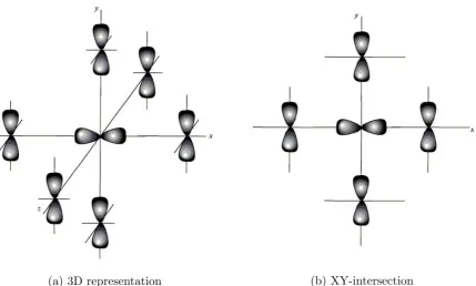
In figure25the p-orbitals are drawn with ψx(r) in the center and it’s nearest neighbors ψy(r−
R). Figure 25b shows the XY-plane, in wich ψx(r) at the origin is even and the nearest neigbors (ψy(r −R)) are odd. Therefore the overlap integrals between ψx(r) and ψy(r −R) forR=a(±1,0,0) anda(0,±1,0) are zero. In figure25a it can be seen that this is the case for
ψx(r) and all it’s nearest neighbors. The same argument can be made for the other off-diagonal terms, therefore all off-diagonal terms are zero.
(a) 3D representation (b) XY-intersection
Figure 25: 3D representation (figure 25a) and XY-intersection (figure 25b) of the p-orbitals in a simple cubic lattice for an atom at the origin and it’s nearest neighbors. The atom at the origin is a px state while the nearest neighbors are py states. Based on [16]
Figure 27: 3D representation of the p-orbitals of an atom at the origin of a face centered cubic lattice and it’s nearest neighbors. The atom at the origin is a px state while the nearest neighbors arepy states. Based on [16]
(a) ΓX-direction (b) ΓL-direction
Figure 30: Sketches of the energy of the p-bands along the ΓX direction and the ΓL direction. The band are calculated for a face centered cubic crystal using tight binding.
0 0.2 0.4 0.6 0.8 1
−15 −10 −5 0 5 10 15
k y [2π/a]
ε
[eV]
ε1(k) ε2(k)
(a) ΓX-direction
0 0.1 0.2 0.3 0.4 0.5
−16 −14 −12 −10 −8 −6 −4 −2 0 2 4
(k
x, ky, kz)/(2π/a)
ε
[eV]
ε1(k) ε2(k)
(b) ΓL-direction
Figure 31: Numerically solved energy bands in the ΓX-direction and the ΓL-direction. The calculations are made for a face centered cubic crystal using thight binding. They were based on equations (91) and (93).
Problem 2 - Numerical diagonalization
For this problem, the energy bands are calculated by setting up a loop over all k-points along the ΓX and ΓL-directions and solving equations (91) and (93) numerically.
In the case of equation (91) (ΓX) this can be done quite easily because the matrix is already diagonal. The energy bands that were calculated in this case are given in figure 31a. In this figure, the x-axis contains the values forky from 0 to 2πa in units of 2πa , while the y-axis contains the energy ε(k). The values of Ep and β were set to zero while for γ0 and γ2 a value of 1 eV was used. Only two energy bands are shown because ε1(k) is double degenerate.
Using a LAPACK subroutine the eigenvalues of the matrix in equation (93) (ΓL) can be deter-mined numerically. In figure 31b the energybands in the ΓL direction are plotted. Again, the x-axis is in units of 2πa and the y-axis contains the energy ε(k). This time however, the bands are plotted along the line where kx = ky = kz from 0 to πa. In this case also, Ep and β were set to zero, while for γ0, γ1 and γ2 a value of 1 eV was used. Again, only two energy bands are shown because ε1(k) is double degenerate.
(a) Grapene lattice. The lattice vectors are indicated in red, the basis vectors are indicated in blue and the Wigner-Seitz cell is indicated in green. Based on an image made with VESTA [11].
(b) Reciprocal lattice of the graphene lattice from fig-ure32a. The reciprocal lattice vectors are indicated in red and the first Brillouin zone is indicated in green.
Figure 32: Lattice and reciprocal lattice of graphene.
Assignment 6
This section contains the solutions to the final assignment set from the Theoretical Solid State Physics course.
1. Graphene π bands
(a) A sketch of the lattice can be found in figure 32a. In this figure, the lattice vectors and basis vectors are indicated bya1,a2 andτ1,τ2 respectively. The Wigner-Seitz cell is indicated in green. Two Wigner-Seitz cells are drawn.
The reciprocal lattice vectors are:
b1 = 2π
a (
2
√
3,0,0)
b2 = 2π
a (
1
√
3,1,0)
(96)
The reciprocal lattice is sketched in figure 32b. In this figure the reciprocal lattice vectors are indicated in red and the first Brillouin zone is indicated in green.
Appendix 2 - VASP-calculations
To practice using VASP different band structure and density of states calculations have been done. These results were used to analyze the differences in the electronic properties of materials when one moves in different directions in the periodic table. The result of the calculations were analyzed in a vertical direction (e.g. C→Si→ Ge), a horizontal direction (e.g. C→ BN) and an ‘inward’ direction (e.g. graphite → graphene). The results can be found in this appendix.
For some of the materials calculations were done for multiple structures. Of these structures the total energies were also calculated. One has to keep in mind that the total energies of the different materials cannot be compared, since all the materials have a different potential. Only values for the same material in different structures can be compared.
Carbon
For carbon calculations were done for diamond, graphite and graphene, one layer of graphite. After the different paragraphs containing the results of these calculations the total energies of the different structures are compared.
Diamond VASP calculations were done for carbon in it’s diamond structure. The resulting band structure and density of states can be found in figure34. The plotted path was L-Γ-X-K-Γ and the density of states and the band structure plot share the same energy axis. The Fermi energy was set to zero and is marked in the figure by a dotted line. For these calculations a PBE potential was used.
The band structure along the L-Γ-X path was calculated by Gl¨otzel et al. [17] for an energy range of −13 to 17 eV. The results from figure 34 can thus be compared to their results. The only differences in the results are at points where the bands cross, but it is known that VASP can give a strange result at band crossings since the software is designed to avoid these crossings.
The band gap calculated in this case was around 4.2 eV, while it should be 5.5 eV [18]. This can be explained by the fact that VASP uses density functional theory for it’s calculations, which underestimates the band gap of materials.
Graphite The band structure and density of states for graphite were calculated using a PBE and a LDA potential and are plotted in figures 35and 36respectively. In these plots the band structure and density of states share the same energy axis which is zero at the Fermi energy (dotted line). The band structure calculations were done along the path Γ-M-K-Γ-A-L-H-A.
L Γ X K Γ -20
-10 0 10
Energy [eV]
0 0.5 1 1.5
Density of states
Figure 34: Band structure and density of states for diamond along the L-Γ-X-K-Γ path. The Fermi energy has been set to zero and is marked by a dotted line.
structures are the same except for the fact that Kobayashi [19] calculated more valence bands. The energy values at the high symmetry points were compared and are the same as far as one can determine by eye.
Graphite is a semi-metal [20] so the band gap should be zero. However, the band structure shows a gap of 0.02 eV in figure 36. These problems can be explained by the fact that when these calculations are done, the charge densities are calculated first for which the k-points are generated automatically. In this case, the charge densities were never calculated explicitly at the K point, the location of the band gap. Therefore, at this point the band structure was interpolated resulting in a band gap.
The difference in the band structures calculated using a PBE and a LDA potential are plotted in figure 37. The differences are mostly between two matching bands and always smaller than 0.4 eV.
Graphene The band structure and density of states have been calculated for graphene, a monolayer of graphite, using VASP with a PBE and LDA potential. These plots can be found in figure 38 for the PBE potential and figure 39 for the LDA potential. In both figures the density of states is plotted along the path Γ-M-K-Γ. The Fermi energy has been set to zero and is marked with a dotted line. The band structure shares it’s energy axis with the density of states plot.
Γ M K Γ A L H A -20
-10 0 10
Energy [eV]
0 1 2 3 4
Density of states
Figure 35: Band structure and density of states for carbon in a hexagonal structure, also known as graphite. The band structure is plotted along the Γ-M-K-Γ-A-L-H-A path. The Fermi energy has been set to zero and is marked by a dotted line. Calculations were done by VASP using a PBE potential.
Γ M K Γ A L H A
-20 -10 0 10
Energy [eV]
0 1 2 3 4
Density of states
Γ M K Γ A L H A -20
-10 0 10
Energy [eV]
Figure 37: Band structures for graphite calculated using a PBE (black) and LDA (red) po-tential. They have the same x and y axis scaling to show the differences between the two calculations.
Table 2: Total energy per atom for three different carbon structures.
Total energy per atom [eV]
PBE LDA
Diamond −9.0894745
Graphite −9.20588925 −10.1130285 Graphene −9.217241 −10.09413
The total energies of the three different structures are listed in table 2. It contains the to-tal energy per atom in eV for the three different structures and the two different potentials. Calculations for diamond with a LDA potential were not done.
The PBE calculations in table 2suggest that graphene is the most stable structure of carbon. However the LDA calculations suggest that graphite is more stable than graphene. This could be explained by the fact that VASP doesn’t take the van der Waals forces between the graphene sheets in graphite into account. This might explain why according to the PBE calculations graphite is less stable than graphene while in reality one would never encounter a sheet of graphene.
Γ M K Γ -20
-10 0 10
Energy [eV]
0 0.5 1 1.5 2
Density of states
Figure 38: Band structure and density of states for one sheet of graphite, also known as graphene. The band structure is plotted along the Γ-M-K-Γ path. The Fermi energy has been set to zero, marked by the dotted line. Calculations were done by VASP using a PBE potential.
Silicon
Diamond structure After carbon VASP calculations were done for silicon, which has a diamond structure. The band structure of silicon for the path L-Γ-X-K-Γ was plotted in figure41along with the density of states. The density of states plot shares it’s energy axis with the band structure plot. The Fermi energy has been set to zero and is marked with a dotted line. A PBE potential was used in the calculations.
The band structure for the L-Γ-X path in the energy range from −8 to 6 eV is compared to a calculation of the band structure of silicon by Gl¨otzel et al. [17]. The band structures are the same except for some strange crossings as was the case with diamond.
The band gap for silicon is 1.11 eV [21]. From figure 41 one can determine a band gap of around 0.5 eV. This is again because density functional theory calculations underestimate the band gap.
Germanium
Γ M K Γ -20
-10 0 10
Energy [eV]
0 0.5 1 1.5 2
Density of states
Figure 39: Band structure and density of states for graphene using a LDA potential. The band structure is plotted along the Γ-M-K-Γ path. The Fermi energy has been set to zero, marked by the dotted line.
The differences between the band structures are small as can be seen in figure 44. The biggest difference might be that the band structure shows no band gap at all for the LDA potential calculation, although the density of states shows a band gap of around 0.08 eV. Besides this the valence bands are not always exactly the same, but the differences are smaller than 0.2 eV. The band gap for germanium should be 0.66 eV [21], but the difference can again be blamed on density functional theory.
Gl¨otzel et al. [17] also calculated the band structure for germanium along the L-Γ-X path in the energy range from −10 to 4 eV. Again there are some differences because of the crossings. Also, the band gap in figure42is smaller but Gl¨otzel et al.[17] moved their lowest energy band at the gamma point up a little bit. The rest of the band structure matches.
Boron nitride
The calculations for boron nitride were done for four different structures, that is for the zinc blende, wurtzite and hexagonal structure and for a monolayer of the hexagonal structure. After the results of the different calculations the total energies of these structures are compared.
Γ M K Γ -20
-10 0 10
Energy [eV]
Figure 40: Band structures for graphene calculated using a PBE (black) and LDA (red) po-tential. They have the same x and y axis scaling to show the differences between the two calculations.
L-Γ-X-K-Γ.
The band structure can be compared to calculations done by Abdulkareem and Elias [22]. They plotted the band structure along the path L-Γ-X-Γ. The band structure they found matches the band structure in figure 45. The calculated band gap is 4.45 eV in this case, but is again underestimated. Chrenko [23] for example calculated a band gap of 6.4±0.5 eV.
Wurtzite structure Calculations for the wurtzite structure of boron nitride were also done, with the resulting band structure and density of states plotted in figure 46. Calculations were done along the path Γ-M-K-Γ-A-L-H-A, using a PBE potential. The band structure and density of states plot share the same energy axis in the figure. The Fermi level is set to zero and marked by a dotted line.
The band structure can be compared along the path Γ-M-K-Γ-A-L to the band structure calculated by Kobayashi [24]. The band structures seem to match except for at some crossings of the valence bands. Where in figure 46some conduction bands seem to cross, they clearly do not cross in the calculations by Kobayashi [24].
L Γ X K Γ -10
-5 0 5 10
Energy [eV]
0 0.5 1 1.5 2 2.5 3
Density of states
Figure 41: Band structure and density of states for silicon along the L-Γ-X-K-Γ path. The Fermi energy has been set to zero and is marked by the dotted line. The charachter of the bands is shown in this figure, with the p-charachter in blue and the s-character in red.
Hexagonal structure Also for hexagonal boron nitride calculations were done. Just as with the wurtzite structure, the calculations were done along the path Γ-M-K-Γ-A-L-H-A and a PBE potential was used. The resulting band structure and density of states can be found in figure 47. Both plots share the same energy axis. The Fermi energy was set to zero and is marked by the dotted line.
The band structure can also be compared to calculations by Kobayashi [26]. He calculated the band structure along the path Γ-M-K-Γ-A-L. The band structures are the same except that figure 47contains one more conduction band along Γ-M-K-Γ.
The band gap has been calculated by Blase et al. [27]. They calculated a band gap of 5.4 eV. This is bigger than the band gap that can be determined from figure 47, which is 4.25 eV, so it’s again underestimated.
Monolayer Calculations were also done for a monolayer of hexagonal boron nitride, that is one sheet from the hexagonal boron nitride structure. The band structure and density of states were calculated along the Γ-M-K-Γ path using a PBE potential. The results can be found in figure 48. In this figure, the density of states and band structure plot have the same energy axis. The Fermi level was set to zero and is marked by the dotted line.
A band structure calculation was also done by Drummond et al. [9] along the path Γ-K-M-Γ. Comparing the result from figure 48 to their result shows a good resemblance. The band gap determined from figure 48is 4.63 eV, again underestimated since it should be >5.0 eV [13].
L Γ X K Γ -10
-5 0 5 10
Energy [eV]
0 0.5 1 1.5 2 2.5 3
Density of states
L Γ X K Γ -10
-5 0 5 10
Energy [eV]
0 0.5 1 1.5 2 2.5 3
Density of states
Figure 43: Band structure and density of states for germanium along the L-Γ-X-K-Γ path. The Fermi energy has been set to zero and is marked by the dotted line. Calculations were done by VASP using a LDA potential.
L Γ X K Γ
-10 -5 0 5 10
Energy [eV]
L Γ X K Γ -10
-5 0 5 10 15
Energy [eV]
0 0.5 1 1.5
Density of states
Figure 45: Band structure and density of states for boron nitride in a zinc blende structure along the L-Γ-X-K-Γ path. The Fermi energy has been set to zero and is marked by the dotted line.
Table 3: Total energy per atom for four different boron nitride structures.
Structure Total energy per atom [eV]
Zinc blende −8.7106
Wurtzite −8.6900545
Hexagonal −8.77376775
Monolayer −8.7835655
total energy per atom in eV is given. According to these values the monolayer of the hexagonal structure is the most stable. However, just as with graphene, this is most likely wrong because the van der Waals forces are ignored in the calculations.
Therefore it can be concluded from table 3 that the hexagonal structure is the most stable structure. The zinc blende structure comes next and the wurtzite structure is the least stable structure of boron nitride.
Aluminium phosphide
Γ M K Γ A L H A -10
-5 0 5 10 15
Energy [eV]
0 1 2 3 4
Density of states
Figure 46: Band structure and density of states for boron nitride in a wurtzite structure along the Γ-M-K-Γ-A-L-H-A path. The Fermi energy has been set to zero and is marked by the dotted line.
Γ M K Γ A L H A
-10 -5 0 5 10
Energy [eV]
0 0.5 1 1.5 2 2.5 3
Density of states
Γ M K Γ -10
-5 0 5 10 15
Energy [eV]
0 0.5 1 1.5 2 2.5 3
Density of states
Figure 48: Band structure and density of states for a monolayer of hexagonal boron nitride along the Γ-M-K-Γ path. The Fermi energy has been set to zero and is marked by the dotted line.
The results can be compared to band structure calculations by Saliev [28]. He calculated the band structure along the same path. His results match the band structure from figure 49. The band gap determined from figure 49 is 1.5 eV but should be 2.5 eV [29], so the band gap is again underestimated.
Gallium arsenide
Zinc blende structure Next, band structure and density of states calculations were done for gallium arsenide. Just as aluminium phosphide gallium arsenide has a zinc blende structure. The results of the calculations, done using a PBE potential and along the path L-Γ-X-K-Γ, can be found in figure50. The band structure and density of states have the same energy axis. The Fermi level is marked by the dotted line and was set to zero in the plots.
The band structure from figure 50 matches the band structure calculated by Danner [30], although he calculated the band structure for one more high symmetry point. The band gap should be 1.43 eV [21], but is 0.6 eV in figure 50, so it is again underestimated.
Zinc selenide
L Γ X K Γ -5
0 5 10
Energy [eV]
0 1 2 3 4
Density of states
Figure 49: Band structure and density of states for aluminium phosphide along the L-Γ-X-K-Γ path. The Fermi energy has been set to zero and is marked by the dotted line.
L Γ X K Γ
-5 0 5 10
Energy [eV]
0 1 2 3 4 5
Density of states
L Γ X K Γ -5
0 5 10
Energy [eV]
0 1 2 3 4 5 6 7
Density of states
Figure 51: Band structure and density of states for zinc selenide in a zinc blende structure along the L-Γ-X-K-Γ path. The Fermi energy has been set to zero and is marked by the dotted line.
Zinc blende structure The result of these calculations can be found in figure51. The band structure and density of states are plotted there, calculated using a PBE potential. The band structure was calculated along the path L-Γ-X-K-Γ. The energy axis is shared between the band structure and density of states and the Fermi energy was set as zero. The Fermi energy is marked by a dotted line.
The band structure is compared to the band structure calculated by Bernard and Zunger [31] and matches the band structure from figure51. They also give a band gap of 2.8 eV. In figure51 the band gap is 1.32 eV, again underestimated.
Wurtzite structure The last calculation is for zinc selenide in a wurtzite structure. The results of this calculation, done using a PBE potential, can be found in figure 52. In this figure the band structure and density of states are shown with the band structure plotted along the path Γ-M-K-Γ-A-L-H-A. Both these plots share the same energy axis. The Fermi level is set to zero on this axis and is marked by a dotted line.
The band structure can be compared to calculations done by Zakharov et al. [32]. They calculated a different path but parts of it can still be compared. The band structures generally match, but sometimes a doubly degenerate band from figure52isn’t visible in their calculations due to poor resolution. An example of this can be seen in the valence bands between K and Γ.
Γ M K Γ A L H A -5
0 5
Energy [eV]
0 1 2 3 4 5 6 7 8 9 Density of states
Figure 52: Band structure and density of states for zinc selenide in a wurtzite structure along the Γ-M-K-Γ-A-L-H-A path. The Fermi energy has been set to zero and is marked by