Single Board Computers
Programmer’s Reference Guide
(Part 2 of 2)
Notice
While reasonable efforts have been made to assure the accuracy of this document, Motorola, Inc. assumes no liability resulting from any omissions in this document, or from the use of the information obtained therein. Motorola reserves the right to revise this document and to make changes from time to time in the content hereof without obligation of Motorola to notify any person of such revision or changes. No part of this material may be reproduced or copied in any tangible medium, or stored in a retrieval system, or transmitted in any form, or by any means, radio, electronic, mechanical, photocopying, recording or facsimile, or otherwise, without the prior written permission of Motorola, Inc.
It is possible that this publication may contain reference to, or information about Motorola products (machines and programs), programming, or services that are not announced in your country. Such references or information must not be construed to mean that Motorola intends to announce such Motorola products, programming, or services in your country.
Restricted Rights Legend
If the documentation contained herein is supplied, directly or indirectly, to the U.S. Government, the following notice shall apply unless otherwise agreed to in writing by Motorola, Inc.
Use, duplication, or disclosure by the Government is subject to restrictions as set forth in subparagraph (c)(1)(ii) of the Rights in Technical Data and Computer Software clause at DFARS 252.227-7013.
Motorola, Inc. Computer Group 2900 South Diablo Way
Preface
This manual provides board level information and detailed ASIC chip information including register bit descriptions for the MVME166, MVME167, MVME176, MVME177, and MVME187 Single Board Computers. The information in this manual applies to the single board computers listed in the following table:
Notes
This document is bound in two parts. Part 1 (VMESBCA1/PGcontains Chapters 1 through 4. Part 2 (VMESBCA2/PGxx)) contains Chapters 5 through 9.This manual replaces the MVME166/167/187 Single Board Computers ProgrammerÕs Reference Guide, MVME187PG/D3, and its supplement, MVME187PG/D3A1. They are obsolete.
This manual is intended for anyone who wants to program these boards in order to design OEM systems, supply additional capability to an existing compatible system, or work in a lab environment for experimental purposes.
A basic knowledge of computers and digital logic is assumed.
To use this manual, you should be familiar with the publications listed in Related Documentation below.
MVME166 Models
MVME167 Models
MVME176 Models
MVME177 Models
Related Documentation
The following publications are applicable to the Single Board Computers and may provide additional helpful information. If not shipped with this product, they may be purchased by contacting your local Motorola sales ofÞce. Non-Motorola documents may be obtained from the sources listed.
Document Title Publication NumberMotorola
MVME166 Single Board Computer User's Manual MVME166/D MVME167 Single Board Computer User's Manual MVME167/D MVME176 Single Board Computer Installation and Use Manual VME176A/IH MVME177 Single Board Computer Installation and Use Manual VME177A/IH MVME167Bug Debugging Package User's Manual MVME167BUG/D MVME177Bug Diagnostics User's Manual V177DIAA/UM Debugging Package for Motorola 68K CISC CPUs User's
Manual (Parts 1 and 2)
68KBUG1/D and 68KBUG2/D MVME187 RISC Single Board Computer User's Manual MVME187/D MVME187Bug Debugging Package User's Manual MVME187BUG/D Debugging Package for Motorola 88K RISC CPUs User's
Manual
88KBUG1/D and 88KBUG2/D Single Board Computers SCSI Software User's Manual SBCSCSI/D MVME712-06/07/09 I/O Distribution Board Set User's Manual MVME712IO/D MVME712-10 Transition Module User's Manual MVME712-10/D MVME712M Transition Module and P2 Adapter Board
User's Manual
MVME712M/D
MVME712-12, MVME712-13, MVME712A, MVME712AM, and MVME712B Transition Modules and LCP2 Adapter Board User's Manual
Note
Although not shown in the above list, each Motorola ComputerGroup manual publication number is suffixed with characters which represent the revision level of the document, such as Ò/xx2Ó (the second revision of a manual); a supplement bears the same number as a manual but has a suffix such as Ò/xx2A1Ó (the first supplement to the second edition of the manual).The following publications are available from the sources indicated:
Versatile Backplane Bus: VMEbus, ANSI/IEEE Std 1014-1987, The Institute of Electrical and Electronics Engineers, Inc., 345 East 47th Street, New York, NY 10017 (VMEbus SpeciÞcation). (This is also Microprocessor System Bus for 1 to 4 Byte Data, IEC 821 BUS, Bureau Central de la Commission Electrotechnique Internationale; 3, rue de VarembŽ, Geneva, Switzerland.)
Z85230 Serial Communications Controller Data Sheet, order number DC-8293-02, Zilog Inc., 210 East Hacienda Drive, Campbell, CA 95008-6600.
IEEE Standard for Multiplexed High-Performance Bus Structure: VSB, ANSI/IEEE Std 1096-1988, The Institute of Electrical and Electronics Engineers, Inc., 345 East 47th Street, New York, NY 10017 (VSB SpeciÞcation). (This is also Parallel Sub-system Bus of the IEC 821 VMEbus, IEC 822 VSB, Bureau Central de la Commission
Electrotechnique Internationale; 3, rue de VarembŽ, Geneva, Switzerland.) ANSI Small Computer System Interface-2 (SCSI-2), Draft Document X3.131-198X, Revision 10c; Global Engineering Documents, 15 Inverness Way East, Englewood, CO 80112-5704.
CL-CD2400/2401 Four-Channel Multi-Protocol Communications Controller Data Sheet, order number 542400-003; Cirrus Logic, Inc., 3100 West Warren Ave., Fremont, CA 94538.
MC88100 RISC Microprocessor User's Manual MC88100UM MC88200 Cache/Memory Management Unit (CMMU)
User's Manual
MC88200UM
M68040 Microprocessors User's Manual M68040UM M68060 Microprocessors User's Manual M68060UM M68000 Family Reference Manual M68000FR
82596CA Local Area Network Coprocessor Data Sheet, order number 290218; and 82596 User's Manual, order number 296853; Intel Corporation, Literature Sales, P.O. Box 58130, Santa Clara, CA 95052-8130.
DS1643 Nonvolatile Timekeeping RAM, Dallas Semiconductor Data Manual, 4401 South Beltwood Parkway, Dallas, Texas 75244-3292.
NCR 53C710 SCSI I/O Processor Data Manual, order number NCR53C710DM, and NCR 53C710 SCSI I/O Processor ProgrammerÕs Guide, order number NCR53C710PG; NCR Corporation, Microelectronics Products Division, 1635 Aeroplaza Dr., Colorado Springs, CO 80916.
MK48T08(B)/MK48T18(B) TimekeeperTM and 8Kx8 ZeropowerTMRAM data sheet in Static RAMs Databook, order number DBSRAM71; SGS-THOMSON
Microelectronics; North & South American Marketing Headquarters, 1000 East Bell Road, Phoenix, AZ 85022-2699.
i28F008 Flash Memory Data Sheet, order number 290435, i28F020 Flash MemoryData Sheet, order number 290245, i28F008SA Software Drivers Application Note, order number 292095, and i28F008SA Automation and Algorithms Application Note, order number 292099; Intel Literature Sales, P.O. Box 7641, Mt. Prospect, IL 60056-7641. MC68230 Parallel Interface Timer (PI/T) Data Sheet, order number MC68230/D, Motorola Semiconductor Products, Inc., LDC, Broadway Bldg. BB100, P.O. Box 20924, Phoenix, AZ 85036-0924.
Manual Terminology
Throughout this manual, a convention is used which precedes data and address parameters by a character identifying the numeric format as follows:
For example, Ò12Ó is the decimal number twelve, and Ò$12Ó is the decimal number eighteen.
Unless otherwise speciÞed, all address references are in hexadecimal.
An asterisk (*) following the signal name for signals which are level signiÞcant denotes that the signal is true or valid when the signal is low.
$
%
&
dollar
percent
ampersand
specifies a hexadecimal character
specifies a binary number
An asterisk (*) following the signal name for signals which are edge signiÞcant denotes that the actions initiated by that signal occur on high to low transition. In this manual, assertion and negation are used to specify forcing a signal to a particular state. In particular, assertion and assert refer to a signal that is active or true; negation and negate indicate a signal that is inactive or false. These terms are used independently of the voltage level (high or low) that they represent.
Data and address sizes are deÞned as follows:
❏ A byte is eight bits, numbered 0 through 7, with bit 0 being the least significant. ❏ A two-byte is 16 bits, numbered 0 through 15, with bit 0 being the least
significant. For the MVME166, MVME167, MVME176, MVME177, and other CISC boards, this is called a word. For the MVME187 and other RISC boards, this is called a half-word.
❏ A four-byte is 32 bits, numbered 0 through 31, with bit 0 being the least
significant. For the MVME166, MVME167, MVME176, MVME177, and other CISC boards, this is called a longword. For the MVME187 and other RISC boards, this is called a word.
Throughout this manual, it is assumed that the MPU on the MVME187 always programs the CMMUs with big-endian byte ordering, as shown below. Any attempt to use small-endian byte ordering immediately renders the MVME187Bug
debugger unusable.
The terms control bit and status bit are used extensively in this document:
BIT
31 24 23 16 15 08 07 00
ADR0 ADR1 ADR2 ADR3
control bit A bit in a register that can be set and cleared under software control.
true Indicates that a bit is in the state that enables the function it controls
false Indicates that the bit is in the state that disables the function it controls
In all tables, the terms 0 and 1 are used to describe the actual value that should be written to the bit, or the value that it yields when read.
The computer programs stored in the Read Only Memory of this device contain material copyrighted by Motorola Inc., Þrst published 1990, and may be used only under a license such as the License for Computer Programs (Article 14) contained in Motorola's Terms and Conditions of Sale, Rev. 1/79.
!
WARNING
This equipment generates, uses, and can radiate magnetic energy. It may cause or be susceptible to electro-magnetic interference (EMI) if not installed and used in a cabinet with adequate EMI protection.
Motorola¨ and the Motorola symbol are registered trademarks of Motorola, Inc. Delta Series, SYSTEM V/68, SYSTEM V/88, VMEmodule, and VMEsystem are trademarks of Motorola, Inc.
Timekeeper and Zeropower are trademarks of SGS-THOMSON Microelectronics. All other products mentioned in this document are trademarks or registered trademarks of their respective holders.
© Copyright Motorola 1995, 1996 All Rights Reserved
Contents
Chapter 1 Programming Issues
Introduction...1-1
Programming Interfaces...1-1
MC68040 MPU...1-2
MC68060 MPU...1-2
M88000 MPU...1-2
Data Bus Structure...1-2
EPROMs on the MVME167/176/177/187...1-3
MVME167 and MVME187 ... 1-3 MVME176/177 ... 1-3 Flash Memory on the MVME176/177...1-4
Flash Memory and Download EPROM on the MVME166...1-5
SRAM...1-6
Onboard DRAM...1-7
Battery Backed Up RAM and Clock...1-7
VMEbus Interface...1-8
VME Subsystem Bus (VSB) Interface...1-8
I/O Interfaces...1-8
Serial Port Interface... 1-8 MC68230 Parallel Interface/Timer (MVME166/176 Only) ... 1-10 Parallel (Printer) Interface... 1-12 Ethernet Interface ... 1-12 SCSI Interface... 1-13 Local Resources...1-14
Programmable Tick Timers ... 1-14 Watchdog Timer... 1-14 Software-Programmable Hardware Interrupts ... 1-14 Local Bus Time-out ... 1-14 Interrupt Handling...1-15
Interrupt Programming Examples...1-16
M68000 VMEchip2 Tick Timer 1 Periodic Interrupt Example ... 1-17 MVME187 Interrupt Handling... 1-19 Cache Coherency...1-23
Cache Coherency, MVME176/177... 1-23
Cache Coherency, MVME187... 1-24
Using Bus Timers... 1-24
Indivisible Cycles... 1-26
No Supervisor Stack Pointer on MC68060... 1-27
Sources of Local BERR*... 1-27
Local Bus Time-out... 1-28
VMEbus Access Time-out... 1-28
VMEbus BERR*... 1-28
Local DRAM Parity Error... 1-28
VMEchip2... 1-28
VSBchip2 BERR*... 1-29
Bus Error Processing... 1-29
Error Conditions... 1-29
MPU Parity Error... 1-30
MPU Offboard Error... 1-30
MPU TEA - Cause UnidentiÞed... 1-30
MPU Local Bus Time-out... 1-31
DMAC VMEbus Error... 1-31
DMAC Parity Error... 1-31
DMAC Offboard Error... 1-32
DMAC LTO Error... 1-32
DMAC TEA - Cause UnidentiÞed... 1-32
SCC Retry Error... 1-34
SCC Parity Error... 1-34
SCC Offboard Error... 1-34
SCC LTO Error... 1-36
LAN Parity Error... 1-36
LAN Offboard Error... 1-36
LAN LTO Error... 1-37
SCSI Parity Error... 1-37
SCSI Offboard Error... 1-37
SCSI LTO Error... 1-38
Chapter 2 Hardware Configuration
Introduction... 2-1
Fuses...2-2
MVME166 Fuses...2-3
MVME176 Polyswitches...2-3
MVME167/177/187 Fuses...2-3
ConÞguration Jumpers...2-4
ConÞguration Jumpers, MVME166...2-5
ConÞguration Jumpers, MVME167...2-8
ConÞguration Jumpers, MVME177...2-12
ConÞguration Jumpers, MVME187...2-16
ConÞguration Jumpers, MVME176...2-20
Chapter 3 Memory Maps
Introduction...3-1
VMEbus Memory Map...3-1
VSB Memory Map...3-2
Local Bus Memory Map...3-2
Normal Address Range...3-2
Detailed I/O Memory Maps...3-3
Chapter 4 VMEchip2
Introduction...4-1
Summary of Features...4-1
Functional Blocks...4-4
Local Bus to VMEbus Interface...4-4
Local Bus to VMEbus Requester ... 4-8 VMEbus to Local Bus Interface...4-9
Local Bus to VMEbus DMA Controller... 4-11
DMAC VMEbus Requester... 4-13 Tick and Watchdog Timers...4-14
Prescaler... 4-14 Tick Timer ... 4-14 Watchdog Timer... 4-15 VMEbus Interrupter...4-16
VMEbus System Controller...4-17
Reset Driver 4-18
Local Bus Interrupter and Interrupt Handler... 4-18
Global Control and Status Registers... 4-20
VMEboard Functions... 4-20
LCSR Programming Model... 4-21
Programming the VMEbus Slave Map Decoders... 4-26
VMEbus Slave Ending Address Register 1 ... 4-29 VMEbus Slave Starting Address Register 1 ... 4-29 VMEbus Slave Ending Address Register 2 ... 4-29 VMEbus Slave Starting Address Register 2 ... 4-30 VMEbus Slave Address Translation Address Offset Register 1 ... 4-30 VMEbus Slave Address Translation Select Register 1... 4-31 VMEbus Slave Address Translation Address Offset Register 2 ... 4-32 VMEbus Slave Address Translation Select Register 2 ... 4-32 VMEbus Slave Write Post and Snoop Control Register 2... 4-33 VMEbus Slave Address Modifier Select Register 2 ... 4-34 VMEbus Slave Write Post and Snoop Control Register 1... 4-35 VMEbus Slave Address Modifier Select Register 1 ... 4-36 Programming the Local Bus to VMEbus Map Decoders... 4-37
Local Bus Slave (VMEbus Master) Ending Address Register 1 .... 4-40 Local Bus Slave (VMEbus Master) Starting Address Register 1 ... 4-40 Local Bus Slave (VMEbus Master) Ending Address Register 2 .... 4-40 Local Bus Slave (VMEbus Master) Starting Address Register 2 ... 4-41 Local Bus Slave (VMEbus Master) Ending Address Register 3 .... 4-41 Local Bus Slave (VMEbus Master) Starting Address Register 3 ... 4-41 Local Bus Slave (VMEbus Master) Ending Address Register 4 .... 4-42 Local Bus Slave (VMEbus Master) Starting Address Register 4 ... 4-42 Local Bus Slave (VMEbus Master) Address Translation
Address Register 4 ... 4-42 Local Bus Slave (VMEbus Master) Address Translation
Local Bus To VMEbus I/O Control Register ... 4-48 ROM Control Register ... 4-49 Programming the VMEchip2 DMA Controller...4-52
DMAC Registers... 4-53 PROM Decoder, SRAM and DMA Control Register ... 4-54 Local Bus To VMEbus Requester Control Register... 4-56 DMAC Control Register 1 (bits 0-7) ... 4-57 DMAC Control Register 2 (bits 8-15) ... 4-59 DMAC Control Register 2 (bits 0-7) ... 4-60 DMAC Local Bus Address Counter ... 4-61 DMAC VMEbus Address Counter... 4-62 DMAC Byte Counter ... 4-62
Table Address Counter ... 4-63 VMEbus Interrupter Control Register ... 4-63 VMEbus Interrupter Vector Register ... 4-64 MPU Status and DMA Interrupt Count Register ... 4-65 DMAC Status Register ... 4-66 Programming the Tick and Watchdog Timers...4-67
VMEbus Arbiter Time-out Control Register ... 4-67 DMAC Timers and VMEbus Global Time-out Control
Register ... 4-68 VME Access, Local Bus and Watchdog Time-out Control
Register ... 4-69 Prescaler Control Register... 4-70 Tick Timer 1 Compare Register ... 4-71 Tick Timer 1 Counter... 4-71 Tick Timer 2 Compare Register ... 4-72 Tick Timer 2 Counter... 4-72 Board Control Register... 4-73 Watchdog Timer Control Register... 4-74 Tick Timer 2 Control Register ... 4-75 Tick Timer 1 Control Register ... 4-76 Prescaler Counter ... 4-76 Programming the Local Bus Interrupter...4-77
Local Bus Interrupter Enable Register (bits 24-31)... 4-84 Local Bus Interrupter Enable Register (bits 16-23)... 4-85 Local Bus Interrupter Enable Register (bits 8-15)... 4-86 Local Bus Interrupter Enable Register (bits 0-7)... 4-87 Software Interrupt Set Register (bits 8-15) ... 4-88 Interrupt Clear Register (bits 24-31)... 4-88 Interrupt Clear Register (bits 16-23)... 4-89 Interrupt Clear Register (bits 8-15)... 4-90 Interrupt Level Register 1 (bits 24-31)... 4-90 Interrupt Level Register 1 (bits 16-23)... 4-91 Interrupt Level Register 1 (bits 8-15)... 4-91 Interrupt Level Register 1 (bits 0-7)... 4-92 Interrupt Level Register 2 (bits 24-31)... 4-92 Interrupt Level Register 2 (bits 16-23)... 4-93 Interrupt Level Register 2 (bits 8-15)... 4-93 Interrupt Level Register 2 (bits 0-7)... 4-94 Interrupt Level Register 3 (bits 24-31)... 4-94 Interrupt Level Register 3 (bits 16-23)... 4-95 Interrupt Level Register 3 (bits 8-15)... 4-95 Interrupt Level Register 3 (bits 0-7)... 4-96 Interrupt Level Register 4 (bits 24-31)... 4-96 Interrupt Level Register 4 (bits 16-23)... 4-97 Interrupt Level Register 4 (bits 8-15)... 4-97 Interrupt Level Register 4 (bits 0-7)... 4-98 Vector Base Register ... 4-98 I/O Control Register 1 ... 4-99 I/O Control Register 2 ... 4-100 I/O Control Register 3 ... 4-104 Miscellaneous Control Register ... 4-105 GCSR Programming Model... 4-107
Programming the GCSR... 4-109
General Purpose Register 3... 4-115 General Purpose Register 4... 4-116 General Purpose Register 5... 4-116
Chapter 5 VSBchip2
Introduction...5-1
Summary of Features...5-1
Functional Description...5-3
VSB to Local Bus Interface...5-5
VSB Slave Interface ... 5-5 Programmable Map Decoders ... 5-5 Write Post Buffer ... 5-6 Local Bus Master Interface... 5-6 VSB Block Transfer to a Local Bus Burst ... 5-8 Local Bus to VSB Interface...5-8
Local Bus Slave Interface... 5-9 Programmable Map Decoders ... 5-9 Bounce Mode ... 5-9 Write Post Buffer ... 5-10 VSB Master Interface ... 5-11 VSB Dynamic Bus Sizing... 5-11 VSB Timers... 5-11 VSB Block Transfers... 5-12 VSB Requester and VSB Serial Arbiter...5-13
VSB Geographical Addressing... 5-13 VSB Requesters... 5-14 VSB Serial Arbiter ... 5-16 Arbitration Timer ... 5-16 VSB Interrupter...5-16
VSB Interrupt Handler...5-18
Local Bus Interrupter...5-18
Control and Status Registers...5-19
Local Control and Status Registers Programming Model...5-20
Chip Control/Status Register...5-23
Local Interrupt Vector Base Register...5-25
Local Interrupt Status Register...5-26
Local Interrupt Enable Register...5-27
Reserved Register... 5-30
VSB Requester Control/Status Register... 5-31
Timer Control Register... 5-33
Timer Clock Prescaler Register... 5-34
Local Bus Slave 1 Address Range Register... 5-35
Local Bus Slave 1 Address Offset Register... 5-36
Local Bus Slave 1 Attribute Register... 5-36
Local Bus Slave 2 Address Range Register... 5-38
Local Bus Slave 2 Address Offset Register... 5-39
Local Bus Slave 2 Attribute Register... 5-39
Local Bus Slave 3 Address Range Register... 5-41
Local Bus Slave 3 Address Offset Register... 5-42
Local Bus Slave 3 Attribute Register... 5-42
Local Bus Slave 4 Address Range Register... 5-44
Local Bus Slave 4 Address Offset Register... 5-45
Local Bus Slave 4 Attribute Register... 5-45
Reserved Registers... 5-46
Local Error Address Register... 5-47
Prescaler Current Count Register... 5-47
Prescaler Test Register... 5-48
Board Control and Status Registers Programming Model... 5-50
EVSB Attention Register... 5-52
EVSB Test and Set (TAS) Register... 5-54
General Purpose Register 1... 5-55
General Purpose Register 2... 5-55
VSB Error Status Register... 5-56
VSB Interrupt Control Register... 5-57
VSB Interrupt Vector Register... 5-58
VSB Interrupt Enable Register... 5-59
VSB Interrupt Status Register... 5-60
VSB Slave 1 Address Range Register... 5-61
VSB Slave 1 Address Offset Register... 5-61
VSB Slave 1 Attribute Register... 5-62
VSB Slave 2 Address Range Register... 5-65
VSB Slave 2 Address Offset Register... 5-65
VSB Slave 2 Attribute Register... 5-66
Reserved Register... 5-69
Chapter 6 PCCchip2
Introduction...6-1
Summary of Major Features...6-1
Functional Description...6-2
General Description...6-2
BBRAM Interface...6-3
Download ROM Interface (MVME166 Only)...6-3
82596CA LAN Controller Interface...6-4
MPU Port and MPU Channel Attention... 6-4 MC68040-Bus Master Support for 82596CA ... 6-5 LANC Bus Error ... 6-5 LANC Interrupt... 6-6 53C710 SCSI Controller Interface...6-7
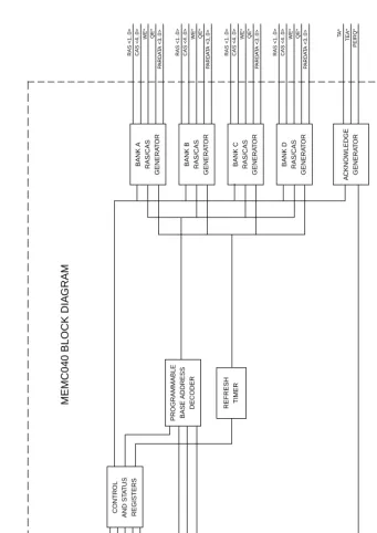
Memory Controller MEMC040 Interface...6-7
Parallel Port Interface...6-7
General Purpose I/O Pin...6-8
CD2401 SCC Interface...6-8
Interrupt Prioritizer (MVME187)...6-10
Tick Timer... 6-11
Overall Memory Map...6-12
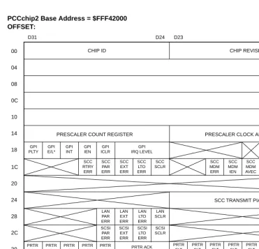
Programming Model...6-13
Chip ID Register...6-16
Chip Revision Register...6-16
General Control Register...6-17
Vector Base Register...6-18
Programming the Tick Timers...6-20
SCC Error Status Register and Interrupt Control Registers... 6-29
SCC Error Status Register ... 6-29 SCC Modem Interrupt Control Register ... 6-30 SCC Transmit Interrupt Control Register ... 6-31 SCC Receive Interrupt Control Register... 6-32 Modem PIACK Register ... 6-33 Transmit PIACK Register ... 6-34 Receive PIACK Register... 6-35 LANC Error Status and Interrupt Control Registers... 6-36
LANC Error Status Register ... 6-36 82596CA LANC Interrupt Control Register ... 6-37 LANC Bus Error Interrupt Control Register ... 6-38 Programming the SCSI Error Status and Interrupt Registers... 6-39
SCSI Error Status Register ... 6-39 SCSI Interrupt Control Register... 6-40 Programming the Printer Port... 6-41
Printer ACK Interrupt Control Register ... 6-41 Printer FAULT Interrupt Control Register ... 6-42 Printer SEL Interrupt Control Register... 6-43 Printer PE Interrupt Control Register ... 6-44 Printer BUSY Interrupt Control Register ... 6-45 Printer Input Status Register ... 6-46 Printer Port Control Register... 6-47 Chip Speed Register ... 6-48 Printer Data Register ... 6-49 Interrupt Priority Level Register ... 6-50 Interrupt Mask Level Register ... 6-51
Chapter 7 MEMC040
Introduction... 7-1
Summary of Features... 7-1
Functional Description... 7-2
General Description... 7-2
Performance... 7-2
Status and Control Registers... 7-5
Register 4 - Alternate Status Register... 7-10 Register 5 - Alternate Control Register ... 7-10 Register 6 - Base Address Register ... 7-10 Register 7 - RAM Control Register ... 7-11 Register 8 - Bus Clock Register... 7-13
Chapter 8 MCECC
Introduction...8-1
Summary of Features...8-1
Functional Description...8-2
General Description...8-2
Performance...8-2
Cache Coherency...8-3
ECC...8-4
Cycle Types ... 8-4 Error Reporting ... 8-5 Single Bit Error (Cycle Type = Burst Read or Non-Burst Read)... 8-5 Double Bit Error (Cycle Type = Burst Read or Non-Burst Read) ... 8-5 Triple (or Greater) Bit Error (Cycle Type = Burst Read or
Non-Burst Read)... 8-6 Cycle Type = Burst Write... 8-6 Single Bit Error (Cycle Type = Non-Burst Write)... 8-6 Double Bit Error (Cycle Type = Non-Burst Write)... 8-6 Triple (or Greater) Bit Error (Cycle Type = Non-Burst Write) ... 8-6 Single Bit Error (Cycle Type = Scrub) ... 8-7 Double Bit Error (Cycle Type = Scrub) ... 8-7 Triple (or Greater) Bit Error (Cycle Type = Scrub)... 8-7 Error Logging...8-7
Scrub...8-7
Refresh...8-8
Arbitration...8-8
Chip Defaults...8-9
Programming Model...8-9
Chip ID Register...8-14
Chip Revision Register...8-14
Memory ConÞguration Register...8-15
Dummy Register 0...8-16
Base Address Register... 8-17
DRAM Control Register... 8-18
BCLK Frequency Register... 8-20
Data Control Register... 8-21
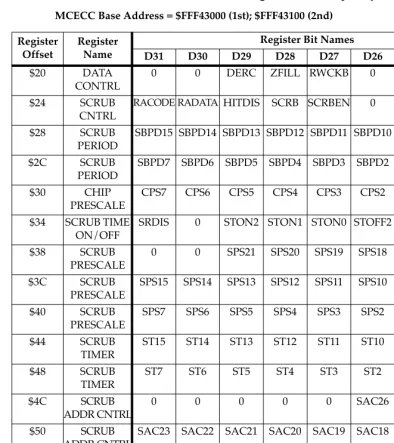
Scrub Control Register... 8-23
Scrub Period Register Bits 15-8... 8-24
Scrub Period Register Bits 7-0... 8-24
Chip Prescaler Counter... 8-25
Scrub Time On/Time Off Register... 8-25
Scrub Prescaler Counter (Bits 21-16)... 8-27
Scrub Prescaler Counter (Bits 15-8)... 8-27
Scrub Prescaler Counter (Bits 7-0)... 8-27
Scrub Timer Counter (Bits 15-8)... 8-28
Scrub Timer Counter (Bits 7-0)... 8-28
Scrub Address Counter (Bits 26-24)... 8-28
Scrub Address Counter (Bits 23-16)... 8-29
Scrub Address Counter (Bits 15-8)... 8-29
Scrub Address Counter (Bits 7-4)... 8-30
Error Logger Register... 8-30
Error Address (Bits 31-24)... 8-31
Error Address (Bits 23-16)... 8-32
Error Address Bits (15-8)... 8-32
Error Address Bits (7-4)... 8-32
Error Syndrome Register... 8-33
Defaults Register 1... 8-33
Defaults Register 2... 8-35
Initialization... 8-36
Syndrome Decode... 8-38
Chapter 9 Printer and Serial Port Connections
Introduction... 9-1
Figures
Figure 1-1. MVME176/177 Flash and EPROM Memory Mapping
Schemes ...1-5
Figure 1-2. MVME187 Interrupt Handling Protocol...1-22
Figure 4-1. VMEchip2 Block Diagram...4-5
Figure 5-1. VSBchip2 Block Diagram...5-4
Figure 6-1. PCCchip2 Block Diagram...6-2
Figure 7-1. Block Diagram for Memory Using MEMC040...7-4
Figure 9-1. MVME167/177/187 Printer Port with MVME712A...9-3
Figure 9-2. MVME167/177/187 Printer Port with MVME712M...9-4
Figure 9-3. MVME167/177/187 Serial Port 1 ConÞgured as DCE...9-5
Figure 9-4. MVME167/177/187 Serial Port 2 ConÞgured as DCE...9-6
Figure 9-5. MVME167/177/187 Serial Port 3 ConÞgured as DCE...9-7
Figure 9-6. MVME167/177/187 Serial Port 4 ConÞgured as DCE...9-8
Figure 9-7. MVME167/177/187 Serial Port 1 ConÞgured as DTE...9-9
Figure 9-8. MVME167/177/187 Serial Port 2 ConÞgured as DTE...9-10
Figure 9-9. MVME167/177/187 Serial Port 3 ConÞgured as DTE... 9-11
Figure 9-10. MVME167/177/187 Serial Port 4 ConÞgured as DTE...9-12
Figure 9-11. MVME167/177/187 Serial Port 1 with MVME712A...9-13
Figure 9-12. MVME167/177/187 Serial Port 2 with MVME712A...9-14
Figure 9-13. MVME167/177/187 Serial Port 3 with MVME712A...9-15
Figure 9-14. MVME167/177/187 Serial Port 4 with MVME712A...9-16
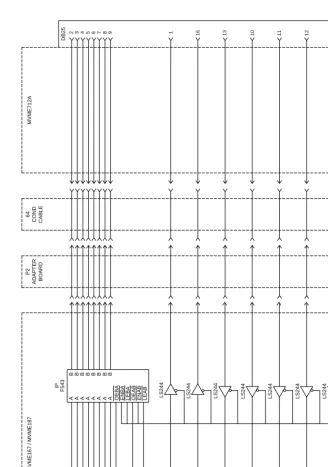
Figure 9-15. MVME166/176 Serial Ports with MVME712-10
(Sheet 1 of 4)...9-17
Figure 9-15. MVME166/176 Serial Ports with MVME712-10
(Sheet 2 of 4)...9-18
Figure 9-15. MVME166/176 Serial Ports with MVME712-10
(Sheet 3 of 4)...9-19
Figure 9-15. MVME166/176 Serial Ports with MVME712-10
Figure 9-16. MVME166/176 Serial Ports with MVME712-06
(Sheet 1 of 3)... 9-21
Figure 9-16. MVME166/176 Serial Ports withMVME712-06
(Sheet 2 of 3)... 9-22
Figure 9-16. MVME166/176 Serial Ports with MVME712-06
Tables
Table 1-1. Single-Cycle Instructions...1-26
Table 2-1. ConÞguring MVME166 Headers...2-5
Table 2-2. ConÞguring MVME167 Headers...2-8
Table 2-3. ConÞguring MVME177 Headers...2-12
Table 2-4. ConÞguring MVME187 Headers...2-16
Table 2-5. MVME176 Headers...2-20
Table 3-1. Local Bus Memory Map...3-4
Table 3-2. I/O Devices Memory Map...3-6
Table 3-3. Cirrus Logic CD2401 Serial Port Memory Map...3-9
Table 3-4. MC68230 PI/T Register Map...3-13
Table 3-5. 82596CA Ethernet LAN Memory Map...3-14
Table 3-6. 53C710 SCSI Memory Map...3-15
Table 3-7. DS1643/MK48T18 BBRAM/TOD Clock Memory Map...3-16
Table 3-8. BBRAM ConÞguration Area Memory Map...3-17
Table 3-9. TOD Clock Memory Map...3-20
Table 4-1. VMEchip2 Memory Map - LCSR Summary (Sheet 1 of 2)...4-22
Table 4-2. VMEchip2 Memory Map - LCSR Summary (Sheet 2 of 2)...4-24
Table 4-3. DMAC Command Table Format...4-53
Table 4-4. Local Bus Interrupter Summary...4-78
Table 4-5. VMEchip2 Memory Map (GCSR Summary)... 4-110
Table 5-1. Local Bus Transfer Size...5-7
Table 5-2. VSBchip2 Local Control and Status Registers Memory Map...5-21
Table 5-3. VSBchip2 Board Control and Status Registers Memory Map....5-50
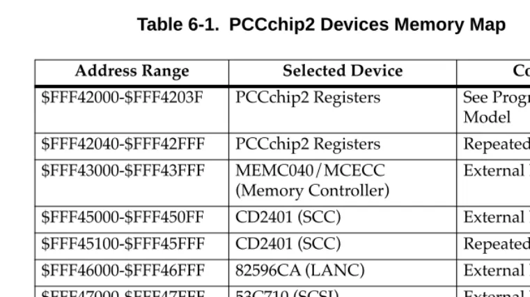
Table 6-1. PCCchip2 Devices Memory Map...6-12
Table 6-2. PCCchip2 Memory Map - Control and Status Registers...6-14
Table 7-1. MEMC040 Performance SpeciÞcations...7-3
Table 7-2. MEMC040 Internal Register Memory Map...7-6
Table 8-1. MCECC Performance SpeciÞcations...8-3
Table 8-2. MCECC Internal Register Memory Map, Part 1... 8-11
5
5
VSBchip2
Introduction
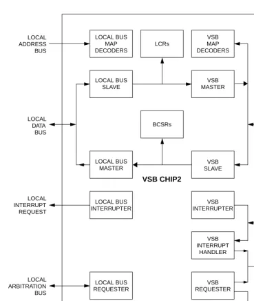
This chapter describes the VSB interface chip ASIC (VSBchip2) used only on the MVME166/176 boards. The VSBchip2 is an ASIC designed to provide a fully functional master/slave interface between the VME Subsystem Bus (VSB) and an MC68040-compatible bus (Local Bus).
Summary of Features
This section lists the major features of the VSB interface chip.
❏ Local Bus to VSB Interface:
Ð Four programmable local bus to VSB map decoders. Each decoder includes a 16-bit address offset register. Independent programmable attributes for each decoder VSB space codes.
Separate read and write enables. Write post enable.
Bounce mode enable.
Ð VSB master generates 8, 16, or 32 bit single- or block-transfer cycles.
Ð Local bus slave accepts 8, 16, or 32 bit single- or burst-transfer cycles.
Ð Supports dynamic bus sizing on VSB. Ð Single level write post buffer.
Ð Programmable timers VSB access timer.
VSBchip2
5
Programmable FAIR request mode.
Programmable release modes (serial mode only): Release When Done (RWD).
Release On Request (ROR).
Programmable Parallel Arbitration ID. Ð Bounce output pin.
Ð Local timer disable output pin.
❏ VSB to Local Bus Interface:
Ð Two programmable VSB to local bus map decoders. Each decoder includes 16-bit address offset register. Independent programmable attributes for each decoder: Participating/Responding slave read and write enables. VSB address space select.
Local bus lock on block transfer enable. Write post enable.
Snoop attribute select. Local bus transfer size select.
Ð Local bus master generates 8, 16, or 32 bit single-transfer cycles.
Ð VSB slave accepts 8, 16, or 32 bit single- or block-transfer cycles.
Ð Additional VSB cycles supported: Data broadcall.
Data broadcast.
Interrupt acknowledge. Ð Single level write post buffer.
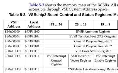
❏ Board Control and Status Register (BCSR) Set:
Ð Supports EVSB Register Set.
❏ Local Interrupter:
Ð Sources
Functional Description
5
VSB Write post error. VSB IRQ asserted.
VSB serviced locally requested interrupt. EVSB Attention Register ATTN bit set.
Ð Independent programmable control over each source:
❏ VSB interrupter:
Ð Sources
VSB Interrupt Status Register VSWIF bit set. VSB Write Post Error.
Ð Unique vector for each source. Ð Programmable FAIR request mode.
❏ VSB interrupt handler:
Ð Parallel multi-source handler with programmable arbitration ID.
Ð VSB IACK cycles generated automatically in response to a local IACK cycle servicing the VSB IRQ asserted interrupt. Ð Programmable local vector used if VSB IACK cycle fails.
Functional Description
5
VSB to Local Bus Interface
The VSB to local bus interface allows a VSB device access to local bus resources. This module includes the VSB slave interface, two programmable map decoders, write post buffer, and local bus master interface.
VSB Slave Interface
The VSB slave interface includes one fixed map decoder, two programmable map decoders, and a write post buffer. To support EVSB, the Board Control and Status Registers (BCSRs) are designed to overlay a non-volatile memory which contains board specific information. The VSBchip2 supports this by giving the fixed map decoder precedence over the programmable map decoders. If one of the programmable map decoders is set to respond to an address also covered by the fixed map decoder, the fixed map decoder is the only one to respond.
In some multi-processing situations, it may be beneficial to perform broadcast and broadcall operations. To support this, the VSBchip2 VSB slave interface can be programmed to act as a participating slave as well as a responding slave.
The VSBchip2 can also be programmed to respond to only read transfers, to only write transfers, or to both. Additionally, it can be programmed to reside in any of the three VSB Address Spaces: System (SAS), Alternate (ALTAS), and/or I/O (IOAS).
Programmable Map Decoders
The VSBchip2 includes two programmable map decoders that allow software to configure the VSB addressing range of local bus resources. The decoders allow the local address range to be
VSBchip2
5
decoder is an attribute register which controls each bank's local bus transfer size, local bus snoop codes, local bus lock, VSB
participating/responding slave enable, VSB read enable, VSB write enable, VSB Address Space, and VSB write posting capability.
Write Post Buffer
The VSB slave can be programmed to perform write posting operations. When in this mode, the chip latches incoming VSB data and addressing information into a write post buffer and
immediately acknowledges the transfer. The VSB is then free for transfers between other devices while the VSBchip2 requests control of the local bus, waits for a local bus grant, and completes the write transfer. The write post buffer stores the data from one byte, word, or longword data transfer. If any VSB to local bus transfer begins before a previous write-posted cycle has completed, that transfer is not acknowledged until the previous write-posted cycle has completed.
Write posting should only be enabled when bus errors are not expected. Using the programmable map decoders, write posting can be enabled for ÒsafeÓ areas and disabled for areas which are not ÒsafeÓ. If the VSBchip2 detects a bus error during a write posted cycle, this condition is reflected in the Local Interrupt Status Register and the VSB Interrupt Status Register, and a local bus and/or a VSB interrupt may be generated. The address contained in the write post buffer is saved in the VSB Error Address Register, and the specific cause of the error is recorded in the VSB Error Status Register.
Local Bus Master Interface
5
One of the programmable attributes for each VSB map is the local bus transfer size. This feature was included because the local bus does not directly support dynamic bus sizing. In some applications, there may be an 8- or 16-bit device on the local bus. By
programming the local bus transfer size appropriately, a VSB device could communicate with the local device without restricting VSB transfer sizes. The local bus master will take care of translating the VSB transfers to the appropriate size on the local bus as shown in Table 5-1.
Table 5-1. Local Bus Transfer Size
Port Size LBTS VSIZE VAD VASACK* LSIZ
1 0 1 0 1 0 1 0 1 0
No Response 1 1 X X X X 1 1 X X
8-bit 1 0 X X X X 1 0 0 1
16-bit 0 1 0 1 X X 0 1 0 1
0 1 1 0 X 0 0 1 1 0
0 1 1 1 X 0 0 1 1 0
0 1 0 0 X 0 0 1 1 0
0 1 1 0 X 1 0 1 0 1
0 1 1 1 X 1 0 1 0 1
0 1 0 0 X 1 0 1 0 1
32-bit 0 0 0 1 X X 0 0 0 1
0 0 1 0 0 0 0 0 1 0
0 0 1 0 0 1 0 1 0 1
0 0 1 0 1 0 0 0 1 0
0 0 1 0 1 1 0 0 0 1
0 0 1 1 0 0 0 1 1 0
0 0 1 1 0 1 0 1 0 1
0 0 1 1 1 0 0 0 1 0
0 0 1 1 1 1 0 0 0 1
0 0 0 0 0 0 0 0 0 0
0 0 0 0 0 1 0 1 0 1
0 0 0 0 1 0 0 0 1 0
VSBchip2
5
VSB Block Transfer to a Local Bus Burst
The VSB slave is capable of receiving VSB block transfer cycles. Each data transfer in the VSB block sequence appears on the local bus as an individual transfer. This is not the most efficient use of VSB block transfers, but unfortunately, because there is no way to know how large the block transfer is going to be, it is not possible to translate these to local bus burst transfers.
Each programmable map can be programmed to lock the local bus during VSB block transfer cycles. This mode can improve data throughput by circumventing the need for local bus arbitration between each data transfer. On VSB it is not possible to determine if a block transfer is in progress until after the first data transfer is complete. After the first data transfer, the negation of PAS* can be used to detect the end of a block. When in local bus lock mode, on the first data transfer of a block, the local bus master acquires the local bus, transfers the data, but does not release the local bus. On subsequent data transfers, the local master can perform transfers without the delay normally caused by acquiring the local bus. After the last cycle of the locked transfer has been completed, the local bus is released.
Note This mode should be used with care. For very long VSB
block transfers, local bus devices could be locked off the local bus too long.
Local Bus to VSB Interface
5
Local Bus Slave Interface
The local bus slave includes four independent programmable map decoders and two fixed map decoders. The two fixed map decoders are used to decode the addresses of the Local Control and Status Registers (LCSRs) and the Board Control and Status Registers (BCSRs) respectively.
When a local bus address falls within the range of one of the programmable map decoders, the VSBchip2 assumes control over the local bus time-out using its internal VSB access and VSB transfer timers. The local bus slave asserts the LBTODIS* output pin to turn off any external timers for the remainder of this transfer.
Programmable Map Decoders
The VSBchip2 includes four map decoders that allow software to configure the local bus addressing range of VSB resources. The decoders allow the VSB address range to be partitioned into four separate banks, each with its own start and end address (in increments of 64 KB). Each map decoder includes a 16-bit offset register. The contents of the offset register are added to the upper 16 bits of the incoming local bus address before the address is passed on to the VSB master. This allows the address of VSB resources to differ from their local address. Associated with each decoder is an attribute register, which controls each bank's VSB space codes and write posting capability.
Bounce Mode
Bounce mode is a means of prioritizing transfers over VSB and VME, and allows VME and VSB local bus slave mappings to overlap. When bounce mode is enabled, VSB assumes the higher priority, and each transfer is attempted on VSB first. If the transfer fails on VSB, it is then attempted on VME.
VSBchip2
5
until it detects the end of the current local bus transfer. If bounce mode is not enabled, the local bus slave asserts LTEA* to terminate the transfer. The BOUNCE output pin is asserted 1 clock after the local bus TS* is detected for cycles which are not decoded by the VSBchip2.
For local bus burst transfers, BOUNCE is asserted only if the Òno responseÓ condition occurred on the first transfer attempt on VSB. On subsequent transfers, the Òno responseÓ condition is treated as a bus error, and the local burst is terminated accordingly.
Write Post Buffer
The local bus slave can be programmed to perform write posting operations. When in this mode, the chip latches incoming local bus data and addressing information into a write post buffer and immediately acknowledges the transfer. The local bus is then free to perform transfers between other devices while the VSBchip2 requests control of the VSB, waits for a VSB grant, and completes the write transfer. The write post buffer stores the data from one byte, word, longword, or burst data transfer. If a local bus write transfer begins before a previous write-posted cycle has completed, that transfer is not acknowledged until the previously write-posted cycle has completed.
Write posting should only be enabled when bus errors are not expected. Normal memory cards never return a bus error on a write cycle. However, some ECC memory cards which reside on VSB perform a read-modify-write operation and therefore may return a bus error if there is an error on the read portion of a read-modify-write. Using the programmable map decoders, write posting can be enabled for ÒsafeÓ areas and disabled for areas which are not ÒsafeÓ. If the VSBchip2 detects a bus error during a write-posted cycle, this condition is reflected in the Local Interrupt Status Register, and a local bus interrupt may be generated. The address contained in the write post buffer is saved in the Local Bus Error Address Register, and the specific cause of the error is recorded in the Chip
5
VSB Master Interface
The VSB master supports data broadcast and data broadcall operations on the VSB. If no VSB device is programmed to respond to the current VSB cycle, the VSB master terminates the VSB cycle and passes this information back to the local bus slave.
VSB Dynamic Bus Sizing
The VSBchip2 supports dynamic bus sizing on the VSB. For example, when a local device initiates a D32 access to a VSB slave that only has D16 data transfer capability, the chip executes two word transfer cycles on the VSB and acknowledges the transfer on the local bus side after all requested data has been transferred. This enhances the portability of software because it allows software to run on the system regardless of the physical organization of global memory.
VSB Timers
VSBchip2
5
Normally, if the VSB is not too heavily loaded, the VSB arbiter grants the VSB master the bus before the VSB access timer expires. However, for a heavily loaded bus, or for situations where some circuitry may be broken, the VSB access timer expires, and the current access attempt is suspended. If the VSB access timer expires, the appropriate error bit is set in the Chip Control/Status Register, and either the local bus TEA* is asserted to terminate the cycle (no write posting) or the LWPIF bit in the Local Interrupt Status Register is set (write posted cycle). System software must then decide whether to retry the cycle or record the error.
The VSB transfer timer is included to guard against lockup due to certain hardware failures. Normally, the VSB address broadcast phase is terminated when each VSB slave releases AC to high. If, however, any slave continues to drive this signal low, the timer expires, and the transfer is aborted. During the VSB data transfer phase, the responding and/or participating slaves assert ACK* and release WAIT*. If, for some reason, one of these signals is stuck or not driven correctly, the VSB transfer timer expires, and the cycle is aborted. If the VSB transfer timer expires, the appropriate error bit is set in the Chip Control/Status Register, and either the local bus TEA* is asserted to terminate the cycle (no write posting) or the LWPIF bit in the Local Interrupt Status Register is set (write posted cycle).
VSB Block Transfers
The VSBchip2 attempts to generate VSB block transfer cycles when multiple VSB transfers are necessary due to a local bus burst transfer.
Local bus burst cycles are not required to be burst aligned (i. e., on even 16-byte boundaries). The local bus address determines the destination of the first longword. The destination of the next longword is determined by incrementing the address by four, unless incrementing by four would cross an even 16-byte
boundary. If a boundary would be crossed, the destination address ÒwrapsÓ back to the previous 16-byte boundary. For example, for a local bus burst which begins at address $00003214, the four
5
$00003218, $0000321C, $00003210 respectively. Because each VSB block transfer must be to the next linear address, it may be necessary to divide local bus burst transfers into at least two VSB blocks. In the example above, the first three longwords could be sent as a block on VSB, but the fourth longword would require the VSB address to be reissued. Each local bus burst transfer is
converted into a VSB block transfer sequence until the address ÒwrapsÓ back to the beginning of the local bus burst boundary. At this point, the VSB address is reissued and a new block begun. If at any time the responding and/or participating VSB slave wishes to break a block transfer sequence, the VSBchip2 reissues the VSB address and starts another VSB block.
VSB Requester and VSB Serial Arbiter
The VSBchip2 contains all the necessary circuitry to implement a serial VSB requester, a serial VSB arbiter, and a parallel VSB requester. The arbitration mode used is determined by the state of the VPARMD* input pin and the geographical address input pins (VGA2 - VGA0) upon power-up. Parallel VSB requester mode is supported by the MVME166/176.
VSB Geographical Addressing
The VSB specification assigns each slot in a VSB backplane a unique address using the GA2 - GA0 signals. When a board is installed in a backplane slot, it uses the addresses on these lines as part of its interrupt and parallel arbitration IDs and to determine which board contains the active VSB arbiter. In addition, the VSBchip2 uses the geographical address to determine the placement of the Board Control and Status Registers. The VSB specification defines the geographical addresses as follows:
VSB Slot GA2 GA1 GA0
1 0 0 0
2 0 0 1
3 0 1 0
4 0 1 1
5 1 0 0
VSBchip2
5
Note VSB must be implemented using a VSB backplane. A typical VSB backplane presses on the back of the VMEbus backplane behind P2.
The VSBchip2 VGA2 - VGA0 input pins have internal pull-up resistors. If they are not connected to the appropriate VSB
geographical addresses, they will always read as %111, an illegal combination according to the VSB specification. In this case, the VSBchip2 assumes it resides in a system without geographical addresses. Parallel arbitration is disabled regardless of the state of the VPARMD* pin, and the serial requester is enabled by default. The VSBchip2 drives VBGOUT* appropriately to configure the rest of the VSB subsystem requesters. The serial arbiter is enabled if software initializes SGA2 - SGA0 in the Chip Control/Status Register to %000. It is the responsibility of the system software to assure that each board in the VSB subsystem is configured with a unique geographical address and that one of those boards is at %000.
If the VGA2 - VGA0 input pins are not %111 after power-up, the VSBchip2 assumes it is in a system with a fully VSB-compliant backplane. If VGA2 - VGA0 are %000, the VSBchip2 samples the VPARMD* input pin to determine the request mode. It then drives the VBGIN*/VBGOUT* daisy chain appropriately to configure the other requesters in the system. If the VPARMD* pin is low, parallel arbitration mode is selected. Systems integrators must be aware that if the board in VSB slot 1 is configured as a parallel requester, all other boards in that VSB subsystem MUST also have parallel requester capability. If serial only boards are placed in a system configured for parallel request mode, the VSB subsystem may become deadlocked.
VSB Requesters
5
each requester submits its bus request to one system arbiter. Only the arbiter in VSB slot 1 (SGA2 - SGA0 are %000) will be the active system arbiter. All other serial arbiters are disabled.
The VSB requester issues a bus request under the following conditions:
The VSB master wishes to perform a VSB cycler, OR
Some external circuitry has asserted the DWB* input pin, OR
System software has set the DWB bit in the VSB Requester Control Register.
The VSB requester may be programmed to implement a ÒfairnessÓ mode to assure that all VSB masters have equal access to the VSB. In fairness mode, any requester which has just released the VSB refrains from requesting it again until VBREQI* is high, indicating no other requests are pending.
When operating in the serial mode, the VSB requester may be programmed to implement one of two different release modes: Release-When-Done (RWD) or Release-On-Request (ROR). Release-When-Done specifies that the requester does not release the bus until its associated master no longer needs it. Release-On-Request means the requester releases the bus only when its
associated master no longer needs it AND some other requester has a request pending.
When the VSBchip2 is operating in parallel arbitration mode, the active parallel requester generates a VSB parallel arbitration cycle to transfer bus mastership. Each requester which has a request pending drives a 7-bit arbitration vector onto the VSB data bus. This vector is composed of SGA2 - SGA0 from the Chip Control/Status Register appended to VARBID3 - VARBID0 from the VSB
VSBchip2
5
VSB Serial Arbiter
Only one serial arbiter may be active in a VSB subsystem. The VSBchip2 serial arbiter is active only if SGA2 - SGA0 in the Chip Control/Status Register are %000, and serial arbitration mode is selected by driving the input pin VPARMD* to a high.
Arbitration Timer
The VSBchip2 includes an arbitration timer which measures the time between when its arbiter asserts bus grant and when a VSB requester assumes control of the bus. This timer prevents a bus lock-up condition caused when no requester assumes control of the bus after a grant was issued. When the timer expires, the arbiter asserts bus busy temporarily as if it is the responding requester and then re-arbitrates any pending bus requests. The VARTO bit in the Chip Control/Status Register is set each time the arbitration timer expires. An arbitration time-out is not normally treated as a fatal error condition because the arbitration is retried, but continued time-outs may be an indication of a bad VSB arbiter/requester or an improper subsystem configuration.
VSB Interrupter
The VSBchip2 has two sources for generating a VSB Interrupt: a VSB Write Post Error, and the VSWIF bit in the VSB Interrupt Status Register.
The VSB interrupter generates a VSB Write Post Error interrupt every time a VSB write posted cycle is aborted because of a local bus time-out or bus error if the VGIE and VWPIE bits are set in the VSB Interrupt Enable Register enabling the VSBchip2 to assert the output pin VIRQO*.
5
When the VSB interrupter within the VSBchip2 detects the VSB master is executing a VSB interrupt acknowledge cycle, this interrupter responds with the 8-bit vector contained in the VSB Interrupt Vector Register and then clears the interrupt request. The lowest order bit of the interrupt vector is unique for each interrupt source. The VSBchip2 only responds to an interrupt-acknowledge cycle if the VEN bit in the VSB Interrupt Control Register is set.
If there is no active VSB interrupt handler, the interrupt bits may be polled and cleared by system software.
The VSB interrupter may be programmed to implement a
ÒfairnessÓ mode to assure that all VSB interrupters have an equal opportunity to be serviced. In fairness mode, any interrupter which has just been serviced refrains from generating another interrupt until VIRQI* is high, indicating no other interrupt requests are pending.
The address broadcast portion of a VSB interrupt acknowledge is used to determine which interrupt is to be serviced. Each interrupt which has a request pending drives a 7-bit arbitration vector onto the VSB data bus. This vector is composed of SGA2 - SGA0 from the Chip Control/Status Register appended to VINTID3 - VINTID0 from the VSB Interrupt Control Register. The interrupt arbitration process is described in the VSB specification section 2.5.4.
After the highest priority interrupt requester has been selected, that requester uses the data transfer portion of the VSB interrupt acknowledge to pass its vector back to the VSB interrupt handler.
Interrupt Vector
Bit 0 Source
VSBchip2
5
VSB Interrupt Handler
The VSB interrupt handler will generate a VSB interrupt acknowledge cycle automatically when it is enabled, a VSB
interrupt is pending, and a local bus interrupt acknowledge cycle is performed to service the VSB interrupt. If no VSB interrupter responds to the VSB interrupt acknowledge cycle, an 8-bit vector derived from the Local Interrupt Vector Base Register will be returned. (Refer to the Local Bus Interrupter description that follows.)
System software is responsible for assuring that only one VSB interrupt handler is enabled in a VSB subsystem at any given time.
Local Bus Interrupter
There are five sources of local bus interrupts: Local Write Post Error, VSB Write Post Error, VSB Interrupt Pending, EVSB Attention Interrupt, and VSB Interrupt Acknowledge Complete. Any of these sources can be programmed to generate a local bus interrupt at any level.
When an interrupt acknowledge cycle is executed to service these interrupts, the vector driven onto the local bus is derived from the Local Bus Interrupt Vector Register as shown below.
A Local Write Post Error interrupt is generated any time an error is detected during completion of a local bus transfer which has been write posted. This interrupt is cleared either automatically when serviced by a local bus interrupt acknowledge cycle or under software control.
Interrupt Vector Bits 3-0 Source
$0 Local Write Post Error Interrupt $1 VSB Write Post Interrupt $2 VSB Interrupt Pending $4 EVSB Attention Interrupt
5
A VSB Write Post Error interrupt is generated any time an error is detected during completion of a VSB transfer which has been write posted. This interrupt is cleared either automatically when serviced by a local bus interrupt acknowledge cycle or under software control.
A VSB IRQ Pending interrupt is generated any time the VSB IRQ signal is asserted. This interrupt can be cleared only by clearing the source of the interrupt on VSB. When this interrupt is serviced by a local bus interrupt acknowledge cycle, the source of the returned vector is programmable. If the VSB interrupt handler is enabled, it performs an interrupt acknowledge cycle on the VSB and passes the resulting vector back to the local bus. If the VSB interrupt handler is disabled or the VSB interrupt acknowledge cycle is unsuccessful, the vector driven onto the local bus is derived from the Local Bus Interrupt Vector Register as shown above.
An EVSB Attention interrupt is generated when the ATTN bit in the EVSB Attention Register is set. This interrupt is cleared either automatically when serviced by a local bus interrupt acknowledge cycle or under software control.
A VSB Interrupt Acknowledge Complete Interrupt is generated when the VSWIF bit in the VSB Interrupt Status Register is cleared. This interrupt is cleared either automatically when serviced by a local bus interrupt acknowledge cycle or under software control. The VSBchip2 includes the means to merge an externally generated prioritized interrupt with those generated internally. When an ex- ternal interrupt is detected on pins LIPLI2 - LIPLI0, its priority level is compared to any pending internal interrupts, and the highest priority level is output on the local bus interrupt level pins LIPLO2 - LIPLO0. This interrupt must be serviced and cleared at its source.
Control and Status Registers
The VSBchip2 includes two sets of registers. The Local
VSBchip2
5
Local Control and Status Registers
Programming Model
The VSBchip2 contains 23 Local Bus Control and Status Registers (LCSRs). These LCSRs are accessible only through the local bus interface. Each register can be read or written by a byte, word, or longword single-transfer cycle. If a burst transfer is used to read from or write to these registers, the first transfer completes successfully and the VSBchip2 asserts LTBI* on the local bus to indicate it cannot complete the rest of the request. Table 5-2
summarizes this register set.
Each register is defined by a table with five lines: an ADR/SIZ field, BIT field, NAME field, OPER field, and RESET field. The ADR/SIZ field defines the base address of the register and the number of bits defined in the table. The BIT field specifies the function's bit location in the register, and the NAME field is the name of the function. Unused bits have the word 'Reserved' in their NAME field. For these bits, writes have no effect and reads always return a zero. The OPER field specifies the allowed operations on that function. These operations are:
The last field, RESET, specifies both the state the bit enters upon application of a reset, and by which reset signal(s) it is affected. The three reset states are 0, 1, or the letter `X' (not affected). The two reset signals are power-up reset (PURST*) signified by the letter 'P', or a local reset (LBRSTI*) signified by the letter 'L'.
5
Table 5-2. VSBchip2 Local Control and Status Registers Memory Map
Local
Address 31 ... 24 23 ... 16 15 ... 8 7 ... 0
$FFF41000 Chip Control/Status Register Local Interrupt Vector Base Register $FFF41004 Local Interrupt Status Register Local Interrupt Enable Register $FFF41008 Local Interrupt Level Register
$FFF4100C Reserved
$FFF41010 VSB Requester Control/Status Register
$FFF41014 Timer Control Register Clock Prescaler Register $FFF41018 Local Slave 1 Address Range Register (NOTES 1,2)
$FFF4101C Local Slave 1 Address Offset Register (NOTE 1) Local Slave 1 Attribute Register (NOTE 1) $FFF41020 Local Slave 2 Address Range Register (NOTES 1,2)
$FFF41024 Local Slave 2 Address Offset Register (NOTE 1) Local Slave 2 Attribute Register (NOTE 1) $FFF41028 Local Slave 3 Address Range Register (NOTES 1,2)
$FFF4102C Local Slave 3 Address Offset Register (NOTE 1) Local Slave 3 Attribute Register (NOTE 1) $FFF41030 Local Slave 4 Address Range Register (NOTES 1,2)
$FFF41034 Local Slave 4 Address Offset Register (NOTE 1) Local Slave 4 Attribute Register (NOTE 1)
$FFF41038 Reserved
$FFF4103C Reserved
$FFF41040 Reserved
$FFF41044 Reserved
$FFF41048 Reserved
$FFF4104C Reserved
$FFF41050 Reserved
$FFF41054 Reserved
$FFF41058 Reserved
$FFF4105C Reserved
$FFF41060 Reserved
$FFF41064 Reserved
$FFF41068 Reserved
$FFF4106C Reserved
$FFF41070 Reserved
VSBchip2
5
Notes 1. Registers listed as ÒSlaveÓ 1, 2, 3, or 4 in this memory
map are listed as ÒMasterÓ 1, 2, 3, or 4 in the ENV
command parameters configurable by MVME166BUG (166Bug) or MVME176BUG (176Bug).
5
Chip Control/Status Register
PURS Power-up Reset Status. This status bit is set when the VSBchip2 undergoes a power-up reset (PURST* asserted). Writing a one clears this bit, and writing a zero does not have an effect.
VLED VSB LED Control. When this bit is cleared, the VSBLED* output pin is driven when either the VSB master has asserted VPAS* or the VSB slave is a responding or participating slave and has obtained control of the local bus. When this bit is set, the VSBLED* output pin is driven only in the latter case - when the VSBchip2 is the local bus master.
VACTO VSB Access Timer Time-out. This bit is set when the VSB Access Timer times out. Writing a one clears this bit, and writing a zero does not have an effect.
VTXTO VSB Transfer Timer Time-out. This bit is set when the VSB Transfer Timer times out. Writing a one clears this bit, and writing a zero does not have an effect.
ADR/SIZ $FFF41000 (8 bits [6 used] of 32)
BIT 31 30 29 28 27 26 25 24
NAME PURS Reserved VLED VACTO VTXTO VARTO VBE
OPER R/C R R/W R/C R/C R/C R/C
RESET 1 P 0 0 0 P 0 PL 0 PL 0 PL 0 PL
ADR/SIZ $FFF41000 (8 bits [6 used] of 32)
BIT 23 22 21 20 19 18 17 16
NAME Reserved VGA2 VGA1 VGA0 Reserved SGA2 SGA1 SGA0
OPER R R R R R R/W R/W R/W
VSBchip2
5
VARTO VSB Arbitration Timer Time-out. This bit is set when the VSB Arbitration Timer times out. Writing a one clears this bit, and writing a zero does not have an effect.
VBE VSB Bus Error. This bit is set when the VSB master detects one of the following three conditions: 1. The VSB responding slave answers by asserting VERRI*.
2. A VSB responding slave is not found at the requested address when bounce mode is disabled. 3. A VSB responding slave does not continue to respond at the requested address after some part of the requested transfer has been completed.
Writing a one clears this bit, and writing a zero does not have an effect.
VGA2 - VGA0 VSB Geographical Address. These bits reflect the status of the VGA2 - VGA0 input pins. An address of %111 indicates that the board is not plugged into a VSB backplane.
SGA2 - SGA0 Programmable Geographical Address. Software can change the board's geographical address by
5
Local Interrupt Vector Base Register
Each interrupt source provides a unique interrupt vector in response to a local bus interrupt acknowledge cycle. LVEC7 - LVEC4 comprise the upper four bits of the vector. LVEC7 is the most sig- nificant bit, and LVEC4 is the least. The lower four bits are unique for each interrupt source. These bits are encoded as shown below:
If the VSBchip2 is programmed as the VSB interrupt handler, it attempts to perform a VSB interrupt-acknowledge cycle on the VSB to obtain the interrupt vector. If, however, the VSBchip2 is not programmed as the VSB interrupt handler, or the VSB device ADR/SIZ $FFF41002 (8 bits [0 used] of 32)
BIT 15 14 13 12 11 10 9 8
NAME Reserved
OPER R
RESET 0 0 0 0 0 0 0 0
ADR/SIZ $FFF41002 (8 bits [4 used] of 32)
BIT 7 6 5 4 3 2 1 0
NAME LVEC7 LVEC6 LVEC5 LVEC4 Reserved
OPER R/W R/W R/W R/W R
RESET 0 P 0 P 0 P 0 P 0 0 0 0
Local Interrupt Source LVEC3 LVEC2 LVEC1 LVEC0 Priority
Local Write Post Error 0 0 0 0 Highest
VSB Write Post Error 0 0 0 1
VSB 0 0 1 0
Reserved 0 0 1 1
EVSB Attention Interrupt 0 1 0 0
VSB Interrupter Acknowledge 0 1 0 1
Reserved 0 1 1 0
Reserved 0 1 1 1
VSBchip2
5
requesting the interrupt is not capable of providing a vector, the VSBchip2 returns the locally generated vector. Software is then responsible for polling the VSB interrupt requesters to determine which requester is to be serviced.
Local Interrupt Status Register
Reading this register returns the status of each interrupt. When a bit is set, it signifies that a local bus interrupt is pending. If that interrupt is enabled through the Local Interrupt Enable Register, a hardware interrupt request is generated. If the interrupt is not enabled, its flag bit can be polled. Once an interrupt flag is set, it can only be cleared by PURST* or LBRSTI* being asserted, software writing a one to it, or a local bus IACK cycle servicing the interrupt.
LWPIF Local Write Post Error Interrupt Flag. This bit is set when an error is detected during completion of a write posted Local Bus cycle. When this flag is set, the Local Bus Error Address Register contains the address at which the write post error occurred. (Refer to this register later in this chapter.)
VWPIF VSB Write Post Error Interrupt Flag. This bit is set when an error is detected during completion of a write posted VSB cycle.
ADR/SIZ $FFF41004 (8 bits [5 used] of 32)
BIT 31 30 29 28 27 26 25 24
NAME Reserved LWPIF VWPIF VSBIF Reserved ATTIF VIAIF Reserved
OPER R R/C R/C R R R/C R/C R
RESET 0 0 PL 0 PL X 0 0 PL 0 PL 0
ADR/SIZ $FFF41004 (8 bits [0 used] of 32)
BIT 23 22 21 20 19 18 17 16
NAME Reserved
OPER R
5
VSBIF VSB Interrupt Flag. This bit reflects the state of the VIRQI* pin.
ATTIF EVSB Attention Interrupt Flag. This bit reflects the state of the BCSR EVSB Attention Register ATTN bit.
VIAIF VSB Interrupt Acknowledge Complete Interrupt Flag. This bit is set only when the VSB Interrupt Status Register VSWIF bit is cleared indicating that the interrupt has been serviced.
Local Interrupt Enable Register
This register is the local bus interrupt enable register. When an enable bit is set, the corresponding interrupt is enabled. When an enable bit is cleared, the corresponding interrupt is disabled. The enable does not clear the interrupt source. If necessary, interrupters should be cleared to remove any old interrupts before being enabled.
GIE Global Interrupt Enable. When this bit is cleared, the interrupts controlled by this register (Local Write Post Error, VSB Write Post Error, VSB Interrupt, EVSB Attention, and VSB Interrupt Acknowledge) are masked, regardless of the state of their
ADR/SIZ $FFF41006 (8 bits [6 used] of 32)
BIT 15 14 13 12 11 10 9 8
NAME GIE LWPIE VWPIE VSBIE Reserved ATTIE VIAIE Reserved
OPER R/W R/W R/W R/W R R/W R/W R
RESET 0 PL 0 PL 0 PL 0 PL 0 0 PL 0 PL 0
ADR/SIZ $FFF41006 (8 bits [0 used] of 32)
BIT 7 6 5 4 3 2 1 0
NAME Reserved
OPER R
VSBchip2
5
individual enable bits. When this bit is set, the five interrupts are not masked and can be enabled by setting their enable bit.
LWPIE Local Write Post Error Interrupt Enable. When this bit and the GIE bit are set, whenever the LWPIF bit in the Local Interrupt Status Register is set, an interrupt is generated on the local bus by asserting its interrupt level programmed in the Local
Interrupt Level Register on the output pins LIPLO2*-LIPLO0*.
VWPIE VSB Write Post Error Interrupt Enable. When this bit and the GIE bit are set, whenever the VWPIF bit in the Local Interrupt Status Register is set, an
interrupt is generated on the local bus by asserting its interrupt level programmed in the Local
Interrupt Level Register on the output pins LIPLO2*-LIPLO0*.
VSBIE VSB Interrupt Enable. When this bit and the GIE bit are set, whenever the VSBIF bit in the Local
Interrupt Status Register is set, an interrupt is generated on the local bus by asserting its interrupt level programmed in the Local Interrupt Level Register on the output pins LIPLO2*-LIPLO0*.
ATTIE EVSB Attention Interrupt Enable. When this bit and the GIE bit are set, whenever the ATTIF bit in the Local Interrupt Status Register is set, an interrupt is generated on the local bus by asserting its interrupt level programmed in the Local Interrupt Level Register on the output pins LIPLO2*-LIPLO0*.
5
Local Interrupt Level Register
These bits define the interrupt level driven onto the output pins LIPLO2*-LIPLO0* to request an interrupt on the local bus. Interrupt level bit 2 (suffix `IL2') is the most significant bit and interrupt level bit 0 (suffix `IL0') is the least significant. There are seven possible levels. Level 7 (%111) is the highest priority level and level 1 ($%001) is the lowest. Level 0 (%000) means the interrupt is disabled.
ADR/SIZ $FFF41008 (8 bits [3 used] of 32)
BIT 31 30 29 28 27 26 25 24
NAME Reserved LWPIL2 LWPIL1 LWPIL0
OPER R/W R/W R/W R/W R R/W R/W R
RESET 0 PL 0 PL 0 PL 0 PL 0 0 PL 0 PL 0
ADR/SIZ $FFF41008 (8 bits [6 used] of 32)
BIT 23 22 21 20 19 18 17 16
NAME Reserved VWPIL2 VWPIL1 VWPIL0 Reserved VSBIL2 VSBIL1 VSBIL0
OPER R R/W R/W R/W R R/W R/W R/W
RESET 0 0 PL 0 PL 0 PL 0 0 PL 0 PL 0 PL
ADR/SIZ $FFF41008 (8 bits [3 used] of 32)
BIT 15 14 13 12 11 10 9 8
NAME Reserved ATTIL2 ATTIL1 ATTIL0
OPER R R/W R/W R/W
RESET 0 0 0 0 0 0 PL 0 PL 0 PL
ADR/SIZ $FFF41008 (8 bits [3 used] of 32)
BIT 7 6 5 4 3 2 1 0
NAME Reserved VIAIL2 VIAIL1 VIAIL0 Reserved
OPER R R/W R/W R/W R
VSBchip2
5
Note The binary levels here are the complement of that