R E S E A R C H
Open Access
Internet-based hardware/software co-design
framework for embedded 3D graphics applications
Chi-Tsai Yeh
1,2*, Chun-Hao Wang
1, Ing-Jer Huang
1and Weng-Fai Wong
3Abstract
Advances in technology are making it possible to runthree-dimensional(3D) graphics applications on embedded and handheld devices. In this article, we propose a hardware/software co-design environment for 3D graphics application development that includes the 3D graphics software, OpenGL ESapplication programming interface
(API), device driver, and 3D graphics hardware simulators. We developed a 3D graphicssystem-on-a-chip(SoC) accelerator usingtransaction-level modeling(TLM). This gives software designers early access to the hardware even before it is ready. On the other hand, hardware designers also stand to gain from the more complex test benches made available in the software for verification. A unique aspect of our framework is that it allows hardware and software designers from geographically dispersed areas to cooperate and work on the same framework. Designs can be entered and executed from anywhere in the world without full access to the entire framework, which may include proprietary components. This results in controlled and secure transparency and reproducibility, granting leveled access to users of various roles.
Keywords:Hardware/software co-design, SystemC, Electronic system level, Internet, 3D graphics SoC, Heteroge-neous hardware interface, Virtual machine
Introduction
3D graphics applications have gained significant popular-ity in recent decades. The market for both 3D graphics gaming applications and 3D video applications on mobile platforms is growing rapidly. The requirements as well as capabilities of consumer electronics such as personal digital assistants(PDAs), cell phones,global positioning
systems (GPSs), and immersive teleconferencing vary
significantly. In particular, screen sizes, resolutions, real-time and energy requirements differ. It is therefore chal-lenging to meet such diversity all within certain design time.
System-level design has attracted much attention because of its ability to cope with the growing complex-ity of designs. Designing in this way raises the level of abstraction of the primary specification, allowing designers to explore the architectural trade-offs and hardware/software partition decisions that need to be made at a higher level. Nevertheless, the solution being
developed is usually just a part of a larger eco-system that consists of other hardware and software.
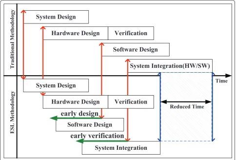
Electronic system-level (ESL) design and verification [1], shown in Figure 1, has been proposed to shorten the development time of embedded applications. The use of ESL can also help designers to meet some of the challenges mentioned previously.
The TLM interface standard [2] provides an essential ESL mechanism for architecture analysis, software devel-opment, software performance analysis, and hardware ver-ification by separating computation and communication. Classifications of TLM are can be found in [3]. Pasricha et al. [4] demonstrated how the TLM approach can be used to model an SoC platform for architecture exploration.
System-level design languages(SLDLs) allow designers to represent of a system at multiple levels of abstraction. Two leading SLDLs, SystemC [5] and SpecC [6], support TLM using the channel concept. SystemC has garnered the most industry support in the United States, while SpecC lacks industry support [7]. SystemC is a modeling language built on top of standard C++ by extending the language with class libraries. Kogel et al. [8] used SystemC in exploring the design space of a 3D graphics processor. * Correspondence: [email protected]
1
Department of Computer Science and Engineering, National Sun Yat-Sen University, Kaohsiung, Taiwan
Full list of author information is available at the end of the article
They implemented a system architecture that could cope with the demands of 3D graphics processing and its internal memory bandwidth requirements. Crisu et al. [9,10] presented a design exploration framework for an embedded 3D graphics accelerator called GRAAL. GRAAL is an open system that offers a coherent develop-ment methodology, based on an extensive library of Sys-temC/register transfer level(RTL) models of graphics pipeline components.
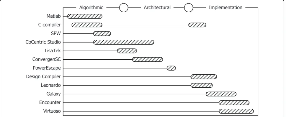
Rupp et al. [11] assume a design process structure con-sisting of an algorithmic, architectural, and implementa-tion stage, as shown in the left-hand side of Figure 2. The design of embedded systems usually starts with the so-called algorithmic stage. Development at the algorithmic stage is aided by such electronic design automation (EDA) tools as Matlab/Simulink, CoWare SPW, and Synopsys CoCentric System Studio. Ram Rajagopal et al. [12] propose a rapid prototyping tool, which leads itself to a very smooth transition from design to implementa-tion, allowing for powerful cosimulation strategies. Ptol-emy [13] shows the importance of using higher-level representation constructs to build real-time functionality. Pelcat et al. [14] present an open-source Eclipse-based
framework, which aims to facilitate the exploration and development processes in this context.
The availability of modeling architectural tools is inade-quate when compared to the other two stages of the design process. The only familiar language at this stage is SystemC, introduced earlier. Synopsys ConvergenSC, which is part of Platform Architect [15], supplies many mature components using SystemC and provides a convenient environment in which integrates SystemC and RTL components.
The Galaxy Implementation Platform [16] is a compre-hensive solution that supports the implementation stage, and is also referred to as the open Milkyway database [17]. This environment is capable of integrating a wide range of Synopsys commercial EDA tools and third-party EDA tools.
Figure 3 presents a recent survey of the most popular EDA tools. As the figure shows, there is no single EDA tool that supports the entire design process from initial concept to final product. The article provides a loose structure of hardware/software co-design. Hardware and software designers facilitate their familiar tools/methods on their own under the proposed environment pre-sented in next section.
System Design
Hardware Design
Verification
Time
Traditional Methodology
ESL Methodology
System Integration
Software Design
Hardware Design
System Design
System Integration(HW/SW)
early verification
Reduced Time
Software Design
early design
Verification
Previous hardware/software co-design frameworks have only considered thedesign-under-test(DUT) appli-cation for hardware components. However, a realistic system usually contains full hardware, consisting of
processors, main memory, vector interrupt controller (VIC), and so on, and full software, such as device dri-vers, anoperating system(OS), APIs, file system, and so on. Thus, additional hardware and software should be
Specs System FunctionalExecutable Model FunctionalSimulation
DUT Hardware DUT Software
Algorithm
HW/SW Partitioning Functional
untimed/timed
Transactional TransactionalCo simulation
Software Test pattern
DUT Hardware DUT Software
Architecture
m
C
TransactionalBehavioral
BCA
Co-simulation
Co-simulation
Other software such as driver, OS, and API Other hardware such as
Processor and memory
Software
Architecture
Syste
m
BCA
RTL
Co-simulation on VM with ISS
Formal Verification
Timing Analysis
Object code
Implementation
V
erilog
Gate Level Netlist
Physical
I l t ti Layout
Co-simulation On Physical board
p
VHDL/
V
Implementation Verificationy
Figure 2Full hardware/software co-design framework during the three stages.
Matlab
SPW
LisaTek CoCentric Studio
ConvergenSC PowerEscape C compiler
Design Compiler Leonardo Galaxy Encounter Virtuoso
Architectural
Algorithmic Implementation
added for building the complete hardware/software co-simulation system, as shown in the middle of Figure 2.
Obviously, it exists a huge gap from a standalone hard-ware/software application to complete system environ-ment. Therefore, the article proposes a framework for hardware/software co-design that permits multiple teams that are geographically dispersed to reproduce each others’ results, and to cooperate in the architecture stage of the design by means of the Internet. This allows the software team to go into development at the earliest possible time.
The rest of the article is organized as follows. We will first describe the concept of our proposed framework and then describe the hardware and software aspects in detail. Followed by our experiment results and reproduces the proposed platform in different parts of the world. Finally, we conclude.
Internet-based hardware/software co-design in the architecture stage
Figure 2 outlines the hardware/software co-design fra-mework. Then, Figure 4 explains in detail the Internet-based co-design method in the architecture stage. In the implementation development stage, a hardware vendor delivers the hard/softintellectual property (IP) core(s) to the software team during their development of the sys-tem. Software designers may need to download a bin stream of an IP core into a field programmable gate
array(FPGA), and then plug the FPGA into a
develop-ment board, for example, VersatilePlatform Baseboard (PB) [B19] and Leopard 6 SoC Design Platform [20], to start software development.
There are significant drawbacks to this process. First, the IPs have to be in place before the software team can start working. This can potentially lengthen the time to market, or corners such as the verification time will have to be cut. Secondly, the software team needs to learn how to use the EDA tools or the FPGA to work on the hardware. This adds new risk factors for verification, because the errors may be caused by the hardware design or simply malfunctions of the FPGA itself. Finally, there is an additional cost factor when using EDA tools or FPGA development platforms, especially if the software team does not already possess them.
In our proposed framework, software designers join the system development at the architecture stage, shown in Figure 2. However, because the development environment is the same for everyone involved, the software designers will consider that they co-design with the hardware team at the physical implementation (FPGA) stage.
QEMU [21] provides a full system simulation platform, which includes microprocessors, peripheral devices, memories, interconnection buses, etc., to act as avirtual machine(VM). It is also able to boot and run an unmodi-fied commercial operating system like as Linux.
Jing-Wun Lin et al. [22] proposed a full system simulation that extended the QEMU-SystemC project provided by GreenSocs [23]. They presented a high-performance framework for hardware/software design and co-verification. Unlike their framework, by leveraging virtua-lization, our proposal allows the software designers to run their program on QEMU, serviced by hardware IPs located in another part of the world. This allows the hardware and software teams to reproduce each other’s work rapidly over the Internet. Using a TLM model and the standard protection provided by the Internet allows both sides to hide the content of their IPs, without com-promising any functionality. Both teams can verify their own work using this framework.
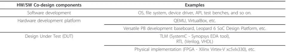
Table 1 shows examples of the hardware and software components. We applied our framework to the design of a 3D graphics hardware accelerator that is integrated in a SoC platform. Using generic 3D graphics application on a workstation, the software team can produce the results they desire without the hardware or a device driver. This allows them to develop the upper layers of the software stack. However, in the lower layers, the device drivers cannot be written and tested without the hardware. Our framework enables the software and hardware teams to adopt a uniform set of test patterns for verifying their designs.
Reproducibility is a key aspect of our framework. It allows for instant feedback on the latest committed design, be it hardware or software, from other members of the team. Yet, the use of TLM means that access to the inner details of each component can be controlled, monitored, and managed. For example, if the hardware team do not wish to reveal an IP to the other members, they can do so by exposing only its interfaces, so that users can still use the component for their own subsystems. The use of the Internet does carry some risks, but there are already a large set of established protocols and mechanisms, such as thesecure sockets layer(SSL) orvirtual private network (VPN), that can minimize any risks caused.
Software development environment
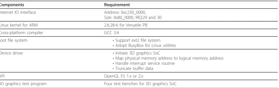
From a software perspective, a full system consists of applications, the operating systems, device drivers, API, etc. In our 3D case study of hardware-software design flow, the software development environment is shown in Figure 5, and the factors of the corresponding com-ponents is shown in Table 2. We explain further the components in the sections below.
Requisition for building guest software environment
guest ARM software environment under host Intel x86 processor. They facilitate cross-platform compiler,GNU Compiler Collection(GCC) [24], to build the guest soft-ware, such as Linux kernel [25,26], Busybox [27], 3D gra-phics device driver, OpenGL ES API, 3D gragra-phics test benches, and so on. Then, the software designers config-ure QEMU platform as Versatile PB and build QEMU as an executable program under host platform. Finally, they execute the software under guest platform QEMU.
3D Graphics Device Driver
According to the 3D graphics test benches shown in Figure 6, The software designers implemented four functions in the device driver. When the user inserts the 3D graphics device driver into the kernel, the function
3D_init_module() allocates the necessary memory
blocks, such as the 3D vertex buffer, 2D vertex buffer, Z buffer, and 32-bit temporary frame buffer. It also informs the Geometry Engine (GE) and theRendering
Table 1 The examples of hardware/software co-design components
HW/SW Co-design components Examples
Software development OS, file system, device driver, API, test benches, and so on.
Hardware development platform QEMU, VirtualBox, etc.
Versatile PB development baseboard, Leopard 6 SoC Design Platform, etc. Design Under Test (DUT) TLM (SystemC - Synopsys EDA tool),
RTL (Verilog, VHDL)
Physical implementation (FPGA - Xilinx Virtex-V xc5vlx330), etc.
a. Architecture Development
b. Implementation Development
root file system
DUT testbenches
Software
development
root file system
DUT testbenches
DUT software stack
DUT software stack
OS
DUT device driver
Vi t l H d e
I t t I/O I t f
Hardware
Ph i l H d e
I/O I t f
OS
DUT device driver
DUT software stack
Virtual Hardware Internet I/O Interface
Internet
development platform
Physical Hardware I/O Interface
Physical signal
DUT
TLM/RTL
FPGA
Engine (RE) modules of the base addresses of these memory blocks.
By calling the mmap()function, the 3D graphics test benches can move 3D vertices into the 3D vertex buffer. After configuring the context table(CT) of the GE, the test benches will enable the GE to start 3D graphics operations. The CT contains the control registers of the GE, while the control registers for the RE are collec-tively known as theregister table(RT).
The 3D graphics SoC provides two interrupt signals that represent the GE and RE, respectively, shown at the bottom of Figure 4. When theinterrupt service routine (ISR) in the device driver receives the GE IRQ, this function will pull down the GEinterrupt request(IRQ), and start the RE to continue the operation immediately.
The RE stores its results in the 32-bit temporary frame buffer, and then raises an IRQ to notify the ISR
of 3D graphics device driver to truncate the pixel data from 32- to 16-bits. The truncation is necessitated by the difference in bit width between the development platform and the 3D graphics SoC. Finally, the 3D gra-phics object is displayed on the output screen.
3D graphics test benches
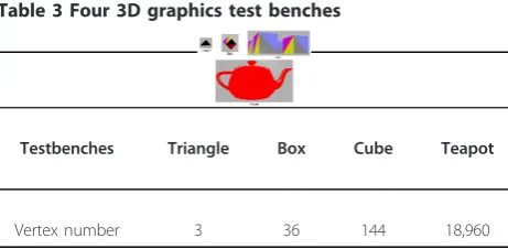
The software designers development two types of 3D graphics test benches. The first type of test benches accesses 3D graphics device driver directly and owns only one object per frame. We have four 3D graphics test benches as shown in Table 3. The first two rows show the images in the test benches, and the last row gives the complexity of these test benches. Each vertex consists of 10 words. Each test bench has four modes, namely, the GE mode, RE mode, single frame mode, and multi-frame mode. The other type of test benches
File system, BusyBox
3D graphics
testbenches
3D graphics
GCC
testbenches
Linux kernel for ARM9
3D graphics driver
OpenGL ES
Guest OS
3D graphics
testbenches
cross com
p
g p
QEMU for Versatile PB
3D graphics SoC
Guest platform
Host OS
Linux for x86
piler
Host platform
Workstation with Intel processor
Linux for x86
Figure 5The software development environment for 3D graphics application.
Table 2 Corresponding configuration list of software development
Components Requirement
Internet IO interface Address: 0xc230_0000, Size: 0x80_0000, IRQ:29 and 30 Linux kernel for ARM 2.6.28-6 for Versatile PB
Cross-platform compiler GCC 3.4
root file system •Support ext2 file system
•Adopt BusyBox for Linux utilities
Device driver •Initiate 3D graphics SoC
•Map physical memory address to logical memory address
•Handle interrupt service routine
•Truncate buffer data
API OpenGL ES 1.x or 2.x
cooperates with OpenGL ES 1.x [28] and owns multiple objects per frame, as shown in Table 4.
The QEMU interface
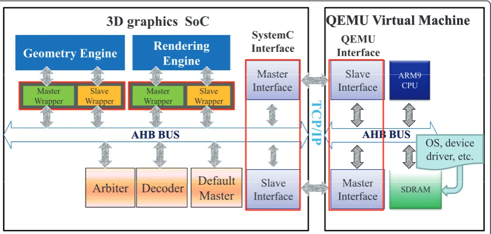
This article leverages the QEMU VM to replace the Versatile PB, thereby facilitating hardware and software co-design. The software stack used on top of the QEMU is shown in Figure 5. The IO interface in the QEMU is similar to theAMBA High-performance Bus (AHB) sys-tem bus that connects the Versatile PB and the FPGA. The latter implements the 3D graphics SoC hardware. This interface is part of the IO interface on the QEMU, as shown on the left-hand side of Figure 7.
The QEMU provides two functions to support master read/write operations. We also considered interrupt handling, and slave read/write operations from the slave interface, used by the 3D graphics SoC. After considering
3D graphics 3D
g p
graphics
testbench
g p
device driver
3D Graphics SoC
2.Open device
1. 3D_init_module
Memory
Data flow Signal flow
3.Call mmap() 4.Map the physical address to logical address
Signal flow Functional
block Storage, IP
block 5. Move Vertex
data and
configure CT/RT 3D vertex buffer
Vertex table
block
6.Geometry Module & Tile Divider
2D vertex buffer
Interrupt
7.Interrupt Service
8.Rendering Engine Z buffer
32’bit Temp Buffer Routine
Interrupt
16’bit Frame Buffer 32 bit Temp Buffer 9. Truncate data
10. Complete a frame
Figure 6The data flow of 3D graphics application.
Table 3 Four 3D graphics test benches
Testbenches Triangle Box Cube Teapot
Vertex number 3 36 144 18,960
Table 4 Experimental results of six 3D graphics testbenches with OpenGL ES 1.x
Singapore Taiwan Ratio
GM Operation Time 7,000 7,000 1.00
GM Data Idle 148,716,120 16,925,520 8.79 GM Wrapper Active 157,076,520 18,584,060 8.45 GM Wrapper Time 160,767,200 18,700,440 8.60
RE Operation Time 26,054,220 2,253,390 11.56 RE Data Idle 8,435,329,980 649,543,730 12.99 RE Wrapper Active 8,495,771,060 653,808,750 12.99 RE Wrapper Time 8,495,839,140 653,876,830 12.99
GE (times) Receive 516
Send 604
RE (times) Receive 26,003
Send 51,385
all the necessary operations, we defined two directions of communication consisting of seven types of operations, as shown in Figure 7.
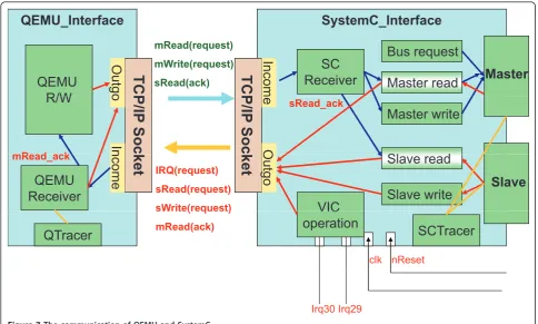
The QEMU interface has three threads that allow it to handle different tasks. The QEMU R/W thread is a main thread provided by the QEMU in charge of pro-cessing the master read/write requests issued from the device driver. This thread will issuemReadRequest
and mWriteRequest requests through an outgoing socket, and receives mReadAck acknowledgment through an incoming socket. The QEMU receiver thread receives any incoming network packages consisting of
IRQRequest, sReadRequest, sWriteRequest, and mReadAck from the SystemC module shown on the right-hand side of Figure 7. The QEMU receiver acts as a slave interface and an interrupt controller. Depending on the content of the messages, it will read or write data from or to the QEMU, raise or pull down an interrupt signal, or pass mReadAck data to the QEMU R/W thread. The connection thread is responsi-ble for maintaining the connection between the QEMU and the SystemC module.
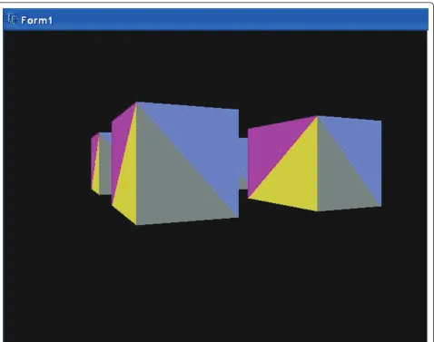
For hardware/software co-verification, a QTracer
module is embedded in the QEMU interface that stores data of the 2D coordinate vertices and frame buffer into a file. The framebuffer viewer is used to output the file,
as shown in Figure 8. The diffcommand can also be used to compare the data to the expected log data [28].
Communication interface and 3D graphics SOC This section introduces the hardware development environment of the proposed co-design framework con-sisting of two hardware parts. Figure 9 presents the block diagram of the full development environment. The first part is the QEMU and the authors create a vir-tual communication between the QEMU and the 3D graphics SoC. In principle, the software and hardware teams work concurrently, but in physical locations that are geographically dispersed. Therefore, the Internet is the best media for maintaining continuous communica-tion between the teams. The second part is the 3D gra-phics SoC itself. This main part of the hardware design is implemented in SystemC using different abstraction levels.
The SystemC interface
The 3D graphics SoC is implemented in SystemC. The block diagram is shown on the left-hand side of Figure 9. We implemented a SystemC interface(SCI) to com-municate with the QEMU viatransmission control pro-tocol/internet protocol(TCP/IP). The SCI acts as a TCP/ IP server that waits for the QEMU requests. The SCI
SystemC_Interface
QEMU_Interface
mRead(request) mWrite(request)
sRead(ack)
TC
Master
P
SC
Receiver
Bus request
Master read
Inco
m
TC
P
Outg
o
QEMU
R/W
P
/IP
Soc
Master write
Sl
d
m
e
O
sRead_ack
P
/IP
Soc
In
o
R/W
R d k
IRQ(request) sRead(request) sWrite(request)
Slave
ket
Slave read
Slave write
VIC
O
utgo
ket
ncome
QEMU
Receiver
mRead_ackclk nReset
sWrite(request) mRead(ack)
VIC
operation
QTracer
SCTracer
contains a master and a slave ports, as well as six main processes as shown on the right-hand side of Figure 7. The master read, master write, slave read, andslave writeprocesses communicate with system bus. The SC receiver process gathers all incoming messages from the QEMU, and forwards them to the corresponding processes. The VIC operationprocess handles interrupts 29 and 30 from the 3D graphics SoC, while the SCTracer records the transactions on the master and slave ports. These can be reproduced later without full software execution. The SCTracer also stores the frame buffer in a file for checking. This will aid in offine debugging and architectural design space exploration.
Figure 10 shows thefinite state machine(FSM) of the AHB master wrapper of the SCI. When the master wrap-per receives a package,Q, from the QEMU that contains anmRead ormWrite command, the FSM will transit from theIdleto theRequeststate. The SCI then calls the different functions provided by the AHB Library to process the master read or write command. To complete anmWriteoperation, the SCI will notify the SC receiver that it has consumed the packet, and so the SC receiver may go ahead and receive another packet. For anmRead
operation, the SCI enters theRead Ackstate, and com-municates the results of the read to the QEMU.
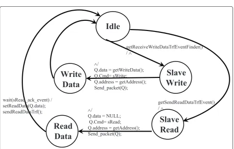
Figure 11 shows the FSM of the AHB slave wrapper in the SCI. Theread dataand write datastates mean that AHB slave wrapper reads data from, or writes data to the QEMU. The SCI sends the packet to the QEMU for read/write data via TCP/IP on the Internet.
However, the state ofread data needs to wait for the QEMU to send a read acknowledgement response.
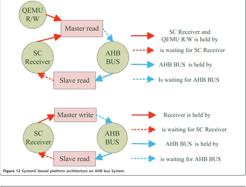
Two types of deadlock
Figure 12 presents the static structure of the SCI, and then Figures 10 and 11 describe the dynamic state tran-sition of the SCI according to the interaction of system operation. However, these figures are unable to detect certain problems, such as deadlocks. Some processes will hold resources, while at the same time requiring other resources held by others. The result is a deadlock. Figure 13 shows two types of deadlock that can happen in the SCI. The first type of deadlock happens when the QEMU wants to read data from the 3D graphics SoC, while at the same time, the 3D graphics SoC also wants to access the QEMU’s memory. The master read process in the SCI holds both the locks for the QEMU read-write in the QEMU interface, and the SC receiver. At the same time, a slave read process requires the SC receiver to return data from the QEMU, and has suc-cessfully locked the AHB bus, resulting in a deadlock. According to our 3D graphics test benches, the master read process usually requires the values of the registers in the 3D graphics SoC.
However, this happens less frequently than the slave read process needs to read data from the 3D graphics SoC. Therefore, to resolve this deadlock, we force the master read process to give up the SC receiver. The SC receiver will record the master read request, and re-request the AHB bus when it is idle. The QEMU will be suspended until this happens.
QEMU Virtual Machine
QEMU Virtual Machine
3D graphics SoC
Slave
ARM9QEMU Virtual Machine
QEMU Virtual Machine
Master
Rendering
Engine
Rendering
Engine
3D graphics SoC
Geometry Engine
Geometry Engine
QEMU
Interface
SystemC
Interface
Slave
Interface
ARM9 CPU
Master
Interface
Master Wrapper
Slave Wrapper Master
Wrapper
Slave
Wrapper
TCP
/
Master
AHB BUS
AHB BUS
Slave
AHB BUS
AHB BUS
OS, device
driver, etc.
Default
/IP
Master
Interface
SDRAMSlave
Interface
Decoder
Arbiter
Default
Master
The second type of deadlock is shown at the bottom of Figure 13. During the time when the application is writing to the control registers, the 3D graphics SoC may concur-rently attempt to read data from the memory of the QEMU. A deadlock occurs as the master write process is unable to lock the bus, but the slave read is unable to complete its data request via the SC receiver. We store the request of the master write process into a cyclic queue to solve this deadlock, because the master write process does not wait for an acknowledgement. This solution results in a race condition between the SC receiver and the master write process as the SC receiver attempts to enqueue while the master write process attempts to dequeue. We solve this problem by making the operations atomic.
The 3D graphics SoC
To take the trade-off between simulation time and accu-racy into account, the 3D graphics SoC mixes two types of
TLM accuracy, namely time-approximate accuracy and bus cycle accuracy(BCA). Time-approximate accuracy of TLM evaluates time information accurately but does not simulate the cycle count actually. BCA is triggered by a cycle event and takes more time than the time-approxi-mate model. The computation of the GE and RE [29] uses time-approximate accuracy. This saves simulation time and provides accurate enough cycle information to hard-ware designers for architecture analysis. Each IP connected to the AHB uses BCA, simulated by Platform Architect from Synopsys, Inc [15]. For instance, the authors gather the time information of thegeometry module(GM) opera-tion to understand the effects of the complexity of the 3D graphics operation. However, they analyze the latency of GM master wrapper to determine the impact of the bus architecture, shown in Figure 14.
Q.Cmd==Idle / wait(SetBusReq_event)
/
consume event notify()
Idle
Q.Cmd=mRead || Q.Cmd==mWrite / SetBusReq_event.notify()consume_event.notify()
Request
Master
~canSendReqTrf()/ wait(SetBusReq_event)
/ setWriteData(Q.data) consume_event.notify()
Write
canSendReqTrf()/sendReqTrf()Q.Cmd==mWrite /
setType(AMBA::tlmWriteAtAddress)
Read
Ack
Address
Master
/ Q.data = getReadData(); Q.Cmd= mRead_ack; Send_packet(Q);
Read
Q.Cmd=mRead /setType(AMBA::tlmReadAtAddress)
Figure 10AHB Master Wrapper FSM in the SystemC interface.
Idle
tR i W it D t T fE tFi d ()
Slave
Write
getReceiveWriteDataTrfEventFinder()
/
/
Q.data = getWriteData();
Slave
Write
Write
Data
wait(sRead ack event) / d d f ()
Q.Cmd= sWrite;
Q.address = getAddress(); Send_packet(Q);
Slave
R d
Read
wait(sRead_ack_event) / setReadData(Q.data); sendReadDataTrf();
getSendReadDataTrfEvent()
/
/
Q.data = NULL; Q.Cmd= sRead;
Q address = getAddress();
Read
Read
Data
Q.address = getAddress(); Send_packet(Q);
AHB
BUS
SC
Receiver
Master read
Slave read
SC Receiver and
QEMU R/W is held by
is waiting for SC Receiver
AHB BUS is held by
Is waiting for AHB BUS
AHB
BUS
SC
Receiver
Master write
Slave read
Receiver is held by
is waiting for SC Receiver
AHB BUS is held by
is waiting for AHB BUS
QEMU
R/W
Figure 12SystemC-based platform architecture on AHB bus System.
the GE is from the 3D vertex buffer and output data is sent to the 2D vertex buffer in main memory. The GE provides a slave wrapper, a GM master wrapper, a tile divider(TD) master wrapper, and an interrupt signal in its interface. The processor configures geometry opera-tion registers (the CT) via the slave wrapper of the GE. The GM master wrapper provides data for the internal GM read from the 3D vertex buffer. The TD master wrapper is dedicated to handle the 2D vertex buffer. When the GE finishes its assigned task, it notifies the QEMU through an interrupt signal.
The GM is responsible for the transformation and light-ing, culllight-ing, and clipping of 3D graphics geometry opera-tions. The TDM is implemented using a tile-based concept [30] so as to reduce the number of memory accesses. The TDM creates tile list data in the 2D vertex buffer for the RE. Output data is passed to the tile divider module, which builds a tiled triangle list for the RE. The GM has three pipeline stages, each about 16 cycles in length. Afirst-in-first-out(FIFO) buffer is needed between the GM and the TDM because of their different speeds. If the FIFO buffer becomes full, then the GM will stall.
The RE consists of three functional modules: the tri-angle setup, the rasterizer, and the per-fragment opera-tions modules, shown in Figure 15. It also adopts a tile-based approach so as to reduce the memory bandwidth. We used a tile size of 32 × 32 pixels, which generally yields the best trade-off between the amount of on-chip memory and the amount of external data traffic. The RE handles three types of data: the 2D vertex buffer, the frame buffer, and the Z/Stencil buffer. The QEMU con-figures the RE’s RT through its slave wrapper. The RE reads data from the 2D vertex buffer and outputs the results to the frame buffer and the Z/Stencil buffer. The
frame buffer stores pixel values, and the Z/Stencil buffer stores the Z/Stencil values. The implementation is designed by the Synopsys EDA tool, shown in Figure 12.
Experiment results
The authors validated their proposed framework in two methods, both for feasibility and reproducibility. The first method is to develop the different applications using the proposed environment, and the other is to reproduce the software development environment at several places. At first, they applied the proposed envir-onment to the different applications, a 3D graphics application and a JPEG decoder, using the general com-munication. There did not have any modification on the SCI and the QEMU interface for these applications.
Then, the authors examine two experiments using the application-specific communication. At first, they suc-cessfully reproduced the software development environ-ment at seven locations and five countries around the world. The second experiment is to validate the feasibil-ity of 3D graphics application and the authors execute six test benches with OpenGL ES API.
General communication
Table 5 shows the simulation result of the proposed fra-mework when developing software in Singapore and Taiwan laboratories separately, while the hardware design is held in a Taiwanese laboratory. The first row represents the locations of developing software. The QEMU will transfers a single command package in each transmission. Each package contains only three words, namely the command type, address, and data. The sec-ond to fifth rows of the table report the simulation results of the GM, and the next four rows are the results
FIFO
Tile Divider
Module
Geometry Module
Slave
Wrapper
GM Master
Wrapper
TD Master
Wrapper
FSM
ContextTable
Vertex Data
Read/Write Write
FIFO Full & Stall
Read/Write
Active Wrapper
Start Ready
Run
Memory, Register, Storage
IP module
Function block
IRQ
Geometry Engine
of the RE. It is obvious that the GM is idle most of the time. The hardware/software co-simulation result is highly dependent on the speed of the network, and it is difficult to perform design space exploration over the network. Performing the experiments locally is 8× to 13× faster than doing it over the Internet. The ninth and tenth rows show the number of receive and send packages in the SCI. The screen size is 640 × 480, and the RE needs to access the frame and Z buffer. There-fore, the number of RE operations far exceed that of GE operations.
The general communication between the QEMU and 3D graphics SoC is transparent to the software/hardware
designers and similar to that between the FPGA and the Versatile PB. Our lab tried to verify the functionality of the new physical development baseboard, Socle Leopard 6 SoC Design Platform [20]. The hardware designer implemented inverse discrete cosine transform(IDCT) [31], a part of JPEG decoder [32], at RTL and download it into its FPGA. Then the software designer wrote an IDCT device driver to transfer data to/from the FPGA. The software designer adopted the proposed develop-ment environdevelop-ment to build the SystemC and RTL co-simulation platform shown in Figure 16 as DUT part of Figure 4. The verification method is to compare the results extracted from IDCT at RTL to the golden
Rasterizer
Slave Wrapper RM Master Wrapper
DMA Triangle List
DMA Pixel & Z Buffer
Triangle Data
Frame Buffer
Bank 1 Bank 0
Context Table
Per-Fragment Operation
Z/Stencil Buffer
Scan Conversion
Z calc.
Color Shading
Texture coordinate
calc.
FSM Controller Triangle
Setup Module
Bank 1
Z/Stencil
Texture Map
Fog
Scissor Al
pha
Bl
endi
ng
Logic-OP
Memory, Register, Storage
IP module
Function block
Bank 0 Wrapper block
IRQ
Figure 15Block diagram of rendering engine[29].
Table 5 The general communication between the QEMU and 3D graphics SoC using SystemC for test bench Box (measured unit: Cycle)
General Communication Application-specific Communication Speedup
GM Operation Time 7,000 7,120 0.98
GM Data Idle 16,925,520 2,050 8256.35
GM Wrapper Active 18,584,060 4,440 4185.60
GM Wrapper Time 18,700,440 6,110 3060.63
RE Operation Time 2,253,390 132,330 17.03
RE Data Idle 649,543,730 2,129,280 305.05
RE Wrapper Active 653,808,750 1,815,960 360.03
RE Wrapper Time 653,876,830 1,984,060 329.57
results generated from the IDCT software module. These designers did not have any knowledge and modi-fication of the QEMU interface and the SCI.
However, the method cannot provide useful cycle information to the hardware designers. The variable evaluation results among the wrappers and execution time is useless for design space exploration. The other problem is the longer simulation time. To resolve this problem, this article proposes another communication, the application-specific communication, in the next section.
Application-specific communication
Figure 6 shows the data flow of the 3D graphics test benches. These test benches generate the 3D vertex data and configure to the GE/RE using the device driver at step 5. After that, GE and RE have numerous R/W operations to different blocks, such as 3D vertex buffer, 2D vertex buffer, Z buffer, and 32’bit frame buffer, in main memory. These memory blocks are reserved for 3D graphics SoC, so no other else will access these blocks. The authors modify the SCI and QEMU inter-face to keep these operation within SystemC side. This modification will not affect the hardware and software design. This communication depends on the data flow of the target application, so it is called as the applica-tion-specific communication. Figure 17 shows the differ-ence in the data flow between the general and the application-specific communication. For instance, when the GE writes data into synchronous dynamic random
access memory (SDRAM) with general communication,
the flow is as follows:
1. The GE writes data on the AHB bus;
2. The SCI receives data, and then forwards them via TCP/IP;
3. The QEMU interface writes data into the specified address;
4. The SDRAM receives the data.
The test bench Box owns 36 vertexes and each vertex occupies 10 words. It means the SCI interface sends 360 read requests to the QEMU at least while the RE at the bottom of Figure 17 reads 3D vertex data from 3D ver-tex buffer at the top of Figure 17 using the general com-munication. However, if the interface designers pack 3D vertex as a package and store them into the SCI as 3D vertex buffer, the only one transmission is needed. In the case of the application-specific communication, the SCI receives data from the GE and stores them into internal buffers. The hardware and software designers can use the application-specific communication without modifying their implementation.
The GE and RE consider the SCI not only as a test bench generator, but also as a memory module compris-ing of the 2D vertex buffer, the Z-buffer, and the frame buffer. When the RE triggers an interrupt signal to the SCI after completing a frame, the SCI moves all the data in the frame buffer to the QEMU interface. The QEMU interface notifies the device driver using interrupt
Behavior Model (QEMU)
TLM (SystemC)
TCP/IP
GE RE
2
1
SC Interface ARM9 DMA
VIC
SDRAM InterfaceQEMU
etc.
3
4
General communication
Application-specific
communication
TCP/IP
GE RE
2
1
SC Interface ARM9 DMA
VIC
SDRAM InterfaceQEMU
etc.
Z buffer
Frame buffer 3D Vertex
2D Vertex
Frame buffer (32b) Z buffer 3D Vertex 2D Vertex
Frame buffer (16b) Frame buffer
(32b) Z buffer 3D Vertex 2D Vertex
Frame buffer (16b)
Behavior Model (QEMU)
TLM (SystemC)
function call on the QEMU platform. The 3D graphics device driver truncates the data from 32- to 16-bits to display them on the QEMU. This processing contains two massive data transmissions: the 3D vertex buffer from the QEMU interface to the SCI, and the frame buf-fer from the SCI to the QEMU interface. Performance is significantly improved. Table 6 shows the comparison between the general and the application-specific commu-nication. The GM data idle time is reduced by over 8,256×, and the total simulation time increased by 29×. Notably, the hardware simulation cycle time is the same no matter where the software test benches are executed in. Because the GM waits for the TD to complete its operation, the time for the GM operation using the gen-eral communication is less than that using the applica-tion-specific communication.
To validate the reproducibility and feasibility of our framework, the authors encapsulated the entire software development environment as a VirtualBox [33] image file, and asked several volunteers at different countries s around the world, such as Singapore, Romania, Austra-lia, England, and USA, to run these experiments. The development environment consists of software develop-ment and hardware developdevelop-ment platform shown in the top of Figure 4a and also owns the four 3D graphics test benches listed in Table 3, with each test bench showing three different frames. The volunteers’environments act as TCP clients, and DUT in Taiwan acts as a TCP ser-ver. We provide not only the VirtualBox image also instruction document on the Internet to the volunteers to execute the instructions step by step. Table 7 shows the results of the geographic differences measured by
IDCT at RTL
IDCT at RTL
S t
C I t f
S t
C I t f
SystemC Interface
SystemC Interface
Figure 17The difference of the data flow among general communication and application-specific communication.
Table 6 Comparison of general and application-specific communication (in cycles) for Box testbench on an entirely local setup
Location of Software Design Triangle Box Cube Teapot
LAN 9/5/5 9/5/5 14/11/11 30/27/26
Taiwan 10/5/5 11/6/5 15/15/15 55/52/48
Singapore 20/11/15 20/15/15 20/20/20 41/40/36
Romania 150/151/151 140/141/145 136/136/132 174/164/165
Australia 20/15/15 16/10/10 25/25/25 50/44/43
London 16/10/10 15/11/10 21/20/20 46/46/44
North Carolina, USA 30/30/25 30/30/30 36/35/31 62/54/60
Eugene, OR, USA 15/10/10 15/10/10 20/15/15 41/34/35
second. The third row, ‘Taiwan,’means that the soft-ware design and the hardsoft-ware design are on different network segments in Taiwan, while ‘LAN’ refers to an entirely local area network setup. The first three test benches own small number of vertexes, so they send the similar number of packages. The latency and stability of the Internet cause the deviation of simulation time.
Our lab have already developed the OpenGL ES 1.x working with our 3D graphics SoC on Versatile PB [28]. The authors migrated these 3D graphics test benches from Versatile PB to our proposed Internet-based plat-form and adjusted the QEMU interface and the SCI to comply with the data flow of these test benches. The results of the six 3D graphics test benches are shown in Table 4. The“Object” field shows the number of objects for each frame, and the“Vertex”field gives the number of the first object that represents the complexity of these testbenches. Finally, the“Time”field presents the simulation time in second using the application-specific communication.
Conclusion
This article proposed an Internet-based hardware/soft-ware co-design framework. The authors have success-fully applied this framework to develop a 3D graphics system-on-a-chip hardware, and the full software stack necessary to use this hardware. Our integrated frame-work achieved the following goals: (1) it provides a full system simulation that includes the hardware as well as the software system; (2) it permits a very early start of concurrent hardware and software development; (3) it
reproduces various test benches of 3D graphics develop-ment by means of theSCTracer; (4) it reproduces the software environment at different places around the world; (5) it adopts application-specific communication to avoid the effect of network transactions achieving a 29.6× increase in speed when compared to general com-munication; and (6) it seamlessly migrates the different abstraction levels, TLM/RTL/FPGA. An important prop-erty of this framework is that someone in a different part of the development process can execute and repro-duce the functionality of another part of the design that was implemented in a geographically remote location. Furthermore, such sharing can be done in a controlled and secure manner. The authors believe that this will significantly increase the productivity of the design teams as a whole.
Abbreviations
AHB: AMBA High-performance Bus; API: application programming interface; BCA: bus cycle accuracy; CT: context table; DUT: design-under-test; DUT: design-under-test; EDA: electronic design automation; ESL: electronic system-level; FPGA: field programmable gate array; FSM: finite state machine; FIFO: first-in-first-out; GE: geometry engine; GM: geometry module; GPSs: global positioning systems; GCC: GNU Compiler Collection; IP: intellectual property; IRQ: interrupt request; ISR: interrupt service routine; IDCT: inverse discrete cosine transform; OS: operating system; PDAs: personal digital assistants; PB: platform baseboard; RT: register table; RTL: register transfer level; RE: rendering engine; SSL: secure sockets layer; SDRAM: synchronous dynamic random access memory; SCI: SystemC interface; SLDLs: system-level design languages; SoC: system-on-a-chip; 3D, three-dimensional; TD: tile divider; TDM: tile divider module; TLM: transaction-level modeling; TCP/IP: transmission control protocol/internet protocol; VM: virtual machine; VPN: virtual private network.
Acknowledgements
The authors would like to thank Himax Technologies Inc. for partially sponsoring our research and thank Professor Chung-Ho Chen of NCKU and his research team for helping the set up of the initial QEMU-SystemC environment. We are also indebted to the volunteers from around the world, including HueySiang Kam in Australia, Mariam Sood in England, Ioana Hagiescu in Romania, Bipasa, CheeWai Lee, and Ding Yang in USA, Wen Chiou in Taiwan, for testing and reproducing our work. This work was partially supported by National Science Council (NSC) of Taiwan, R.O.C. under contrasts NSC 99-2220-E-110-008 and NSC98-2917-I-110-101. Author details
1Department of Computer Science and Engineering, National Sun Yat-Sen University, Kaohsiung, Taiwan2Department of Information Management, Shih Chien University, Taiwan3Department of Computer Science, National University of Singapore, Singapore 117417
Competing interests
The authors declare that they have no competing interests. Received: 1 November 2010 Accepted: 19 July 2011 Published: 19 July 2011
References
1. B Bailey, GE Martin, A Piziali, ESL design and verification: a prescription for electronic system-level methodology (Morgan Kaufmann, 2007) 2. Open SystemC Initiative (OSCI). http://www.systemc.org/home/ 3. L Cai, D Gajski, Transaction Level Modeling: An Overview. inProc of First
IEEE/ACM/IFIP International Conference on Hardware/Software Codesign and
System Synthesis, 19–24 (2003)
Table 7 Experimental results (in seconds) when reproducing at the different places
Cube Door
Object 3 Object 1
Vertex 6 Vertex 1644
Time 14.5 Time 2.5
Multiple cube Teapot
Object 54 Object 7
Vertex 6 Vertex 3000
Time 267.2 Time 37.7
Beethoven Castle
Object 31 Object 36
Vertex 3000 Vertex 3000
4. S Pasricha, N Dutt, M Ben-Romdhane, Extending the Transaction Level Modeling Approach for Fast Communication Architecture Exploration. in
Proc of 41st Design Automation Conference, 113–118 (2004)
5. T Grötker, S Liao, G Martin, S Swan, System Design with SystemC. (Kluwer Academic, Boston, 2002)
6. D Gajski, J Zhu, R Dömer, A Gerstlauer, S Zhao, SpecC: Specification Language and Methodology. (Kluwer Academic, 2000)
7. R Walstrom, J Schneider, D Rover, Teaching system-level design using SpecC and SystemC. inMicroelectronic Systems Education, 2005. (MSE‘05).
Proceedings.2005 IEEE International Conference on, 95–96 (2005)
8. T Kogel, A Wieferink, H Meyr, A Kroll, SystemC Based Architecture Exploration of a 3D Graphic Processor. inProc IEEE Workshop on Signal
Processing Systems, 169–176 (2001)
9. D Crisu, S Cotofana, S Vassiliadis, A Hardware/Software Co-Simulation Environment for Graphics Accelerator Development in ARM-Based SoCs. in Proc 13th Annual Workshop on Circuits, Systems and Signal Processing
(ProRISC’02), 255–268 (2002)
10. B Juurlink, I Antochi, D Crisu, S Cotofana, S Vassiliadis, GRAAL: A Framework for Low-Power 3D Graphics Accelerators. IEEE Comput Graph Appl.28(4), 63–73 (2008)
11. M Rupp, A Burg, E Beck, Rapid prototyping for wireless designs: the five-ones approach. Signal Processing.83(7), 1427–1444 (2003). doi:10.1016/ S0165-1684(03)00090-2
12. R Rajagopal, S Ramamoorthy, L Wenzel, H Andrade, A Rapid Prototyping Tool for Embedded, Real-Time Hierarchical Control Systems. EURASIP Journal on Embedded Systems 2008. 14 (2008)
13. J Buck, S Ha, EA Lee, DG Messerschmitt, Ptolemy: A Framework for Simulating and Prototyping Heterogenous Systems. International Journal in Computer Simulation.4(2), 1–34 (1994)
14. M Pelcat, J Piat, M Wipliez, S Aridhi, J-F Nezan, An Open Framework for Rapid Prototyping of Signal Processing Applications. EURASIP Journal on Embedded Systems 2009. 13 (2009)
15. Synopsys platform architect. http://www.synopsys.com/Systems/ ArchitectureDesign/Pages/PlatformArchitect.aspx
16. Synopsys galaxy implementation platform. http://www.synopsys.com/ Solutions/EndSolutions/GalaxyImplementation/Pages/default.aspx 17. Synopsys milkyway database. http://www.synopsys.com/solutions/
endsolutions/galaxyimplementation/pages/milkyway.aspx
18. P Belanovic, An open tool integration environment for efficient design of embedded systems in wireless communications, PhD thesis, Technische Universität Wien, Wien, Austria. (2006)
19. Versatile Platform Baseboard for ARM926EJ-S™[online]. http://www.arm. com/products/tools/development-boards/versatile/index.php
20. Socle Leopard 6 SoC Design Platform. http://www.socle-tech.com.tw/en/ service_62.html
21. QEMU. http://wiki.qemu.org/Index.html
22. JW Lin, CC Wang, CY Chang, CH Chen, KJ Lee, YH Chu, JC Yeh, YC Hsiao, Full System Simulation and Verification Framework, in Information
Assurance and Security, 2009.IAS‘09 Fifth International Conference on.1,
165–168 (2009)
23. QEMU-SystemC, greensocs. http://www.greensocs.com/en/projects/ QEMUSystemC
24. GCC, the GNU Compiler Collection. http://gcc.gnu.org/ 25. The Linux Kernel Archives. http://www.kernel.org/
26. Creating a virtual build environment. http://people.canonical.com/~ogra/ arm/qemu/kernel/
27. BusyBox. http://www.busybox.net/
28. TY Ho, LB Chen, IJ Huang, An efficient HW/SW integrated verification methodology for 3D Graphics SoC development. inProc of IEEE
International Symposium of Consumer Electronics(ISCE2008). (2009)
29. LB Chen, CT Yeh, HY Chen, IJ Huang, A System-Level Model of Design Space Exploration for a Tile-Based 3D Graphics SoC Refinement, IEICE Transactions on Fundamentals of Electronics. Communications and Computer Sciences E92-A.12, 3193–3202 (2009)
30. I Antochi, B Juurlink, S Vassiliadis, P Liuha, Memory Bandwidth Requirements of Tile-Based Rendering. inProc SAMOS 2004, LNCS 3133. 323–332 (2004)
31. WH Chen, C Smith, S Fralick, A fast computational algorithm for the discrete cosine transform, Communications. IEEE Transactions on.25(9), 1004–1009 (1977). doi:10.1109/TCOM.1977.1093941
32. WB Pennebaker, JL Mitchell, JPEG: Still Image Data Compression Standard. (Springer, 1993)
33. VirtualBox - a general-purpose full virtualizer. http://www.virtualbox.org/
doi:10.1186/1687-6180-2011-25
Cite this article as:Yehet al.:Internet-based hardware/software co-design framework for embedded 3D graphics applications.EURASIP Journal
on Advances in Signal Processing20112011:25.
Submit your manuscript to a
journal and benefi t from:
7Convenient online submission
7Rigorous peer review
7Immediate publication on acceptance
7Open access: articles freely available online
7High visibility within the fi eld
7Retaining the copyright to your article