Design of Application-Specific Instructions and
Hardware Accelerator for Reed-Solomon Codecs
Jung H. Lee
School of Electrical and Computer Engineering, Ajou University, San 5, Wonchun-Dong, Paldal-Gu, Suwon 442-749, Korea Email:[email protected]
Jaesung Lee
Computer System Department, Electronics and Telecommunications Research Institute, 161 Gajeong-Dong, Yuseong-Gu, Taejon 305-350, Korea
Email:[email protected]
Myung H. Sunwoo
School of Electrical and Computer Engineering, Ajou University, San 5, Wonchun-Dong, Paldal-Gu, Suwon 442-749, Korea Email:[email protected]
Received 31 January 2003 and in revised form 6 September 2003
This paper presents new application-specific digital signal processor (ASDSP) instructions and their hardware accelerator to effi -ciently implement Reed-Solomon (RS) encoding and decoding, which is one of the most widely used forward error control (FEC) algorithms. The proposed ASDSP architecture can implement various programmable primitive polynomials, and thus, hardwired RS codecs can be replaced. The new instructions and their hardware accelerator perform Galois field (GF) operations using the proposed GF multiplier and adder. Therefore, the proposed digital signal processor (DSP) architecture can significantly reduce the number of clock cycles compared with existing DSP chips. The proposed GF multiplier was implemented using the Faraday 0.25µm standard cell library and it can perform RS decoding at a rate up to 228.1 Mbps at 130 MHz.
Keywords and phrases:Reed-Solomon, application-specific DSP, GF multiplier, broadband communication, VLSI architecture.
1. INTRODUCTION
With the rapid progress of communication technologies, var-ious broadband access systems have been developed, such as very-high-data-rate digital subscriber line (VDSL) cable mo-dem and wireless LAN, gigabit Ethernet, 4G wireless com-munication, and so forth. Currently, the software defined radio (SDR) can support various communication standards since a common hardware platform can be adapted for var-ious communication standards by means of software [1]. However, ASIC chips face several limitations such as lack of flexibility for various communication standards, high devel-opment costs, and slow time-to-market. Due to these restric-tions, implementation methods have been changed to digital signal processor (DSP)-based communication systems that can have advantages in several aspects [2]. Programmable DSPs are greatly improving time-to-market and allowing faster changes and upgrades than hardwired ASIC chips. In addition, DSPs can be used for various applications as well as the Reed-Solomon (RS) decoder.
RS codes, providing the capability to efficiently correct
burst errors as well as random error, have been extensively used in various communications and digital data storage sys-tems, such as power line communications (PLC) [3], digital video broadcasting terrestrial (DVB-T) system [4], vestigial sideband (VSB) system [5], cable modem [6], satellite and mobile communications [7], magnetic recording [8], and so forth.
g0 g1 g2
· · · g2t−1
Reg. Reg. · · · Reg. p(x)
m0, m1, . . . , mk−1
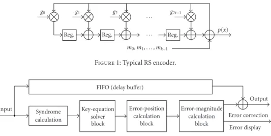
Figure1: Typical RS encoder.
FIFO (delay buffer)
Figure2: Typical RS decoder.
Hence, existing DSP chips have not yet satisfied the require-ments of high-speed communication standards. However, if DSP chips can be made to support the special architec-ture for the RS algorithm, they will be able to implement RS codecs for various communication standards [19]. Thus, having application-specific instructions and their hardware accelerator for the RS algorithm, ASDSP can support various broadband communication standards.
This paper is organized as follows. Section 2 analyzes the implementation and hardware architectures of exist-ing DSP chips [17,18] and custom-designed RS processors [9,10,11,12,13,14,15,16].Section 3describes the pro-posed RS decoding instructions and their hardware acceler-ator.Section 4presents the performance comparisons with existing DSP chips. Finally,Section 5contains conclusions.
2. IMPLEMENTATION OF THE EXISTING DSP-BASED RS DECODERS AND HARDWIRED RS PROCESSORS
This section describes the typical RS processor to briefly re-view the decoding process and analyzes the existing DSP-based implementation of RS.
2.1. Typical RS processor
Depending on the application, a typical RS processor is made up of several hardware blocks for parallel processing. Such an architecture can achieve higher transmission rates than required by current communication standards; however, due to its lack of flexibility regarding the primitive polynomials in various standards, the RS processor has to be redesigned to meet these standards.
2.1.1. RS encoder architecture
The architecture of the RS processor inserts 16 (2t) surplus symbols whent =8. The generator polynomial for this ar-chitecture is represented by (1) [19,20,21]:
g(x)=x+α1x+α2Λx+α2t−1x+α2t
=x+α1x+α2Λx+α15x+α16. (1)
Figure 1shows the typical RS encoder that has the linear feedback shift register (LFSR) structure, based on the gen-erator polynomial. If the architecture is enabled, each regis-ter is initialized as “0.” Afregis-ter the message polynomialm(x) is inserted, the operation is executed by combiningm(x) and g(x) through the LFSR structure. If the insertion of the mes-sage polynomialm(x) is ended, the remaining values in the registers are output as parity symbols.
2.1.2. RS decoder architecture
The RS decoding process is as follows. First, the syndrome value, which is the error pattern, is calculated, and then the error-locator polynomial is calculated to find the error loca-tions. Second, the error values are determined and corrected.
Figure 2illustrates the typical RS decoder [20,21,22,23,24].
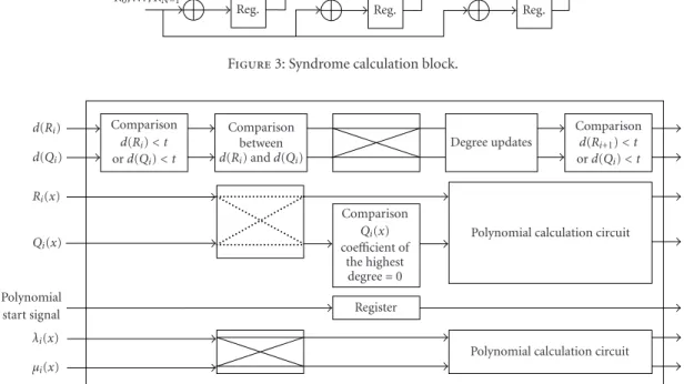
Figure 3shows the syndrome calculation block. The syn-drome is calculated using the roots of the generator polyno-mial (gx), which is used in the encoder. The syndrome poly-nomial presents the error pattern of the received code word. By using this error pattern, the key for error correction is de-coded.
The number of the cells in the syndrome block is twice the number of correctable errors. When the error correction capability (t) of the RS decoder is 8, the number of 2t=16 for the syndrome block is needed, as shown inFigure 3.
R0, . . . , RN−1
Figure3: Syndrome calculation block.
d(Ri)
Figure4: Architecture of the modified Euclid’s algorithm.
algorithm can efficiently reduce the area since it does not re-quire an LUT for the quotient calculation.
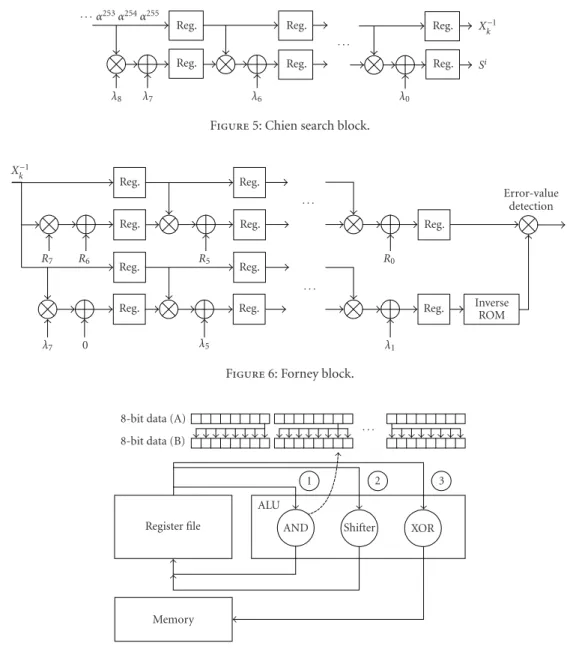
After the error-locator and error-value polynomials are obtained using the Euclid’s algorithm, the error locations are calculated using the Chien search [22,23] and Forney algo-rithms [13]. Then, the error values are calculated. This al-gorithm for calculating the roots of the error-locator poly-nomial is described inFigure 5. The roots of error locations are calculated using the coefficients (λi) of the error-locator polynomial. The error values are computed using the coef-ficients (λi) of the error-locator polynomial and error-value polynomial coefficients (Ri) as shown inFigure 6.
Typical RS ASIC chips require the hardwired GF opera-tion units as modulo multipliers and adders, and thus, the architecture of the GF operation units has to be redesigned based on various primitive polynomials and standards.
2.2. Existing DSP-based RS decoder
It is possible to implement the RS decoder with the existing DSP chip; however, to implement the GF operation with the existing DSP chips, a number of operations are needed to execute ALU operations repeatedly. These operations have to be programmed as a subroutine and this subroutine is called from the GF operation part of the main RS program [20].
Generally, a GF multiplication consists of two steps. In the first step, two equations are multiplied as in (2). If the least significant bit (LSB) of the multiplier is one, the multi-plicand is copied down; otherwise, zeros are copied down. The partial products copied down in successive lines are
shifted one position to the left from the previous partial product. The 15-bit product which is the third equation of (2) is acquired using XOR operations of all partial products. In the second step, the GF operation is executed according to the primitive polynomial to convert the 15-bit data into the 8-bit data. GF multiplications are shown as the “⊗” symbols in Figures 1,3,5, and6. Additions and subtractions in GF operations can be implemented using XOR operations in the ALU:
· · ·α253α254α255
Reg. Reg.
· · ·
Reg. X−1
k
λ8 λ7
Reg.
λ6 Reg.
λ0
Reg. Si
Figure5: Chien search block.
X−1
k
Reg. Reg.
· · ·
Reg. Reg. Reg.
Error-value detection
R7 R6 R5 R0
Reg. Reg.
· · ·
λ7 0
Reg.
λ5
Reg.
λ1
Reg. Inverse ROM
Figure6: Forney block.
8-bit data (A)
8-bit data (B) · · ·
1 2 3
Register file
ALU
AND Shifter XOR
Memory
Figure7: GF multiplication flow of existing DSPs.
To implement this procedure, general purpose DSP chips require quite a number of clock cycles. The DSP used here should be accessible by a bit as well as a byte. If the DSP is a 32-bit machine, it can compute two GF multiply operations. If the DSP is a 64-bit machine, it can compute four GF multi-ply operations simultaneously. IfNALUs can be operated at the same time, 1/Ncycles are taken to compute the GF mul-tiplication. However, if the DSP cannot be accessed by a byte, a number of additional cycles is required.
Hence, we cannot get a fast RS decoding rate since the hardware architecture and instructions are not supported for the GF multiplication on existing DSP chips. Therefore, for the RS decoding, the existing DSP chips can be used only in slow-speed data communication. Recently, TMS320C64x has 8 GF multipliers and the GMPY4 instructions can perform four GF multiplications of two integers, each of which
con-tains 4 packed bytes. Two GMPY4 instructions can be exe-cuted in parallel; hence the 8 GF multiplications can be per-formed in a single cycle. However, it supports only the GF multiply operation [19] and does not support the GF multi-ply and add operations. Moreover, it has a large hardware size and high power consumption due to its VLIW architecture.
SC140 does not support GF operations and is also a VLIW architecture having similar disadvantages. In addition, it consumes more power and needs larger memory since it uses the LUT method [25]. In the implementation using an LUT, the results of GF operations have been stored in ROM or RAM, and they are accessed when they are needed [25]. Whenmis equal to 8, a 28×28 64 Kbytes storage device
Input 1
Input 2
Reg.
Figure8: Repetitive multiply and add operations for the RS codec.
possible. Moreover, additional cycles are needed to access the on-chip and off-chip memories. Hence, most DSPs imple-ment the RS decoding without using an LUT.
3. NEW INSTRUCTIONS AND THEIR ARCHITECTURE
This section presents three instructions for the RS de-coder implementation and the proposed operation flows, and their new architecture. The proposed instructions in-clude modulo-add (MADD), modulo-multiply (MMUL), and modulo-MAC (MMAC).
Various algorithm blocks for RS codecs require repeti-tive multiply and add operations, as shown inFigure 8. The Berlekamp-Massey [9,10] algorithm, the Euclid [11,12] al-gorithm, and the modified Euclid [13,14,15] algorithm also use the circuit shown inFigure 8[9,10,11,12,13,14,15,19] to implement the RS decoding. The multiplier and adder used for RS have the same circuit shown inFigure 8 regard-less of various algorithms or primitive polynomials. The ar-chitecture of the hardwired RS codec is redesigned based on the primitive polynomial. In general, implementing the RS decoder on an existing DSP chip is not effective since the instructions of DSP chips do not support GF multiply and add operations. The GF multiply and add operations, shown inFigure 8, are different from general multiply and add op-erations. Hence, we need an ASDSP chip that has a pro-grammable architecture to support various primitive poly-nomials according to various communication standards.
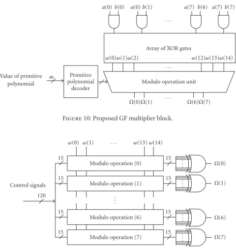
Figure 9represents the proposed MADD, MMUL, and MMAC instructions. The MADD instruction performs the modulo (GF) add operation and can be implemented with an XOR operation of an existing ALU; thus, we do not need additional hardware for the MADD instruction. The MMUL instruction can implement the GF multiply operation for error-value detection with the proposed GF multiplier shown inFigure 10. The proposed GF multiplier can perform suc-cessive GF multiply operations by adding a small amount of extra hardware, consisting of XOR gates and AND gates. The MMAC instruction can perform successive operations of the MADD and MMUL instructions. The MMAC instruc-tion takes one cycle to execute the general modulo MAC in-struction.
The proposed instructions are used extensively in RS al-gorithm blocks, such as the encoder, the syndrome computa-tion block, the modified Euclid’s algorithm block, the Chien
search block, and the Forney algorithm block, as shown in Figures1,3,5, and6. In contrast, TMS320C64x supports the modulo MUL operation but does not support the modulo MAC operation. Hence, the proposed architecture can im-prove the performance of the RS codec.
Figure 10shows the proposed GF multiplier block used for the MMUL and MMAC instructions in GF (2m,m=8). The required number of AND operations shown in the upper side ofFigure 10is the same as the value ofm. InFigure 10, after two 8-bit dataaandbare multiplied, the 15-bitω(i), which is the third equation in (2), is obtained through the modulo add operation of the multiplication results. Then the 8-bit result Ω(i) can be obtained from GF multiply opera-tions of 15-bitω(i).
The proposed GF multiplier uses about 630 gates includ-ing the primitive polynomial decoder. The gate count of the proposed GF multiplier is larger than that of a GF multiplier of the hardwired RS ASIC chip (about 261 gates). However, the hardwired RS ASIC chip uses about 89 GF multipliers fort =8 [13], 16 GF multipliers for the syndrome calcula-tion block, 64 GF multipliers for the modified Euclid’s algo-rithm block, 8 GF multipliers for the Chien search block, and one GF multiplier for the Forney algorithm. The proposed ASDSP uses only 8 proposed GF multipliers, and thus, re-quires a much lower gate count than does the hardwired RS ASIC chip. Therefore, the ASDSP has little extra hardware. When m is greater than 8, the adder can be implemented with additional XOR gates, and the GF multiplier shown in
Figure 10can also be implemented with additional AND and XOR gates.
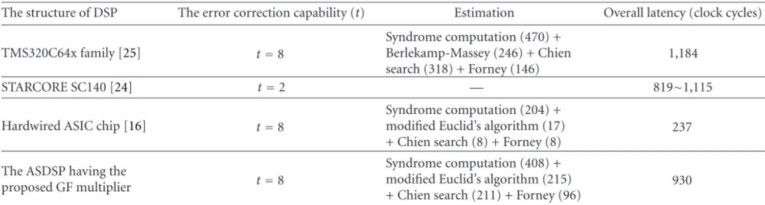
The modulo operation unit shown inFigure 10executes GF operations with control signals according to the value of m and the primitive polynomial.Figure 11 shows the pro-posed modulo operation unit that is designed with AND and XOR gates. The 15-bitω(12) is performed by the XOR op-eration after it is enabled or disabled according to control signals, and then, the 8-bitΩ(i) value can be obtained from the proposed modulo operation unit. Equations (3) are the result value of the GF operation when the primitive polyno-mial isx8+x4+x3+x2+x1andm=8:
The primitive polynomial decoder of the proposed GF multiplier has the information whether theω(i) is enabled or disabled. About 8 cases according tomvalues and the prim-itive polynomials are used in various communication stan-dards. Hence, the decoder receives 3 bits (8 =23) and
Input 1 Input 2
XOR
Output
MADD instruction
Input 1 Input 2
The proposed GF multiplier
Output
MMUL instruction
Input 1 Input 2
The proposed GF multiplier
XOR
Output
MMAC instruction
Input 3
Figure9: The proposed MADD, MMUL, and MMAC instructions.
a(0)b(0) a(0)b(1)
· · ·
a(7) b(6) a(7)b(7)
Array of XOR gates
ω(0)ω(1)ω(2) ω(12)ω(13)ω(14)
· · · Value of primitive
polynomial
m Primitive
polynomial decoder
Modulo operation unit
Ω(0)Ω(1) · · · Ω(6)Ω(7)
Figure10: Proposed GF multiplier block.
ω(0) ω(1) · · · ω(13)ω(14)
15
Modulo operation (0) 15 ... Ω(0)
15
Modulo operation (1) 15 ... Ω(1) Control signals
120 ..
.
15
Modulo operation (6) 15 ... Ω(6)
15
Modulo operation (7) 15 ... Ω(7)
Figure11: Proposed modulo operation unit.
these control signals. The primitive polynomial decoder is designed with combinational circuits. To implement 8 differ-ent combinations using ASIC chips, 8 differdiffer-ent hardware im-plementations are required. However, the proposed ASDSP can efficiently implement these combinations.
Figure 12shows the overall architecture of the proposed ASDSP, based on the modified Harvard architecture. Two 16-bit data memories can be accessed in a single clock cycle since the address generation unit (AGU) generates two addresses. The data processing unit (DPU) consists of two MACs, two ALUs, and one barrel shifter to efficiently support RS. The 8 GF multipliers are also included in DPU. The proposed
AS-DSP employs 7 pipeline stages: prefetch, fetch, decode, exe-cute1, execute2, execute3, and write back. Every instruction, including program control instructions, is executed in a sin-gle cycle. The DO instruction, one of the most frequently used instructions, can also be executed in a cycle.
4. PERFORMANCE COMPARISONS
Ydata bus
Xdata bus
X Y
Ydata
memory
Xdata
memory
Program memory
Inst. bus
Xaddress bus
Yaddress bus
Data processing unit
Register file
MAC MAC
ALU ALU
GF multiplier GF
M1GFM2GFM3GFM4 GF
M5 GF M6
GF M7
GF M8
Accumulator
Figure12: Overall architecture of the proposed ASDSP.
Table1: Performance comparisons of the RS decoding for (204 188 8) RS code in various DSP chips.
The structure of DSP The error correction capability (t) Estimation Overall latency (clock cycles)
TMS320C64x family [25] t=8
Syndrome computation (470) + Berlekamp-Massey (246) + Chien search (318) + Forney (146)
1,184
STARCORE SC140 [24] t=2 — 819∼1,115
Hardwired ASIC chip [16] t=8
Syndrome computation (204) + modified Euclid’s algorithm (17) + Chien search (8) + Forney (8)
237
The ASDSP having the
proposed GF multiplier t=8
Syndrome computation (408) + modified Euclid’s algorithm (215) + Chien search (211) + Forney (96)
930
clock cycles just for a GF multiplication, since it has to repeat the AND, SHIFT, and XOR instructions shown inFigure 7.
Table 1shows the performance comparisons of RS decoding between the ASDSP having 8 proposed GF multipliers shown inFigure 10and the existing DSP chips [17,18,25]. Note that the performance figures of commercial DSP chips are given by their datasheets or references [17,18]. The hardwired RS ASIC takes about 237 cycles fort=8 [16], that is, 204 cycles for the syndrome calculation block, 17 cycles for the mod-ified Euclid’s algorithm block, 8 cycles for the Chien search block, and 8 cycles for the Forney algorithm.
The proposed architecture takes one clock cycle per MMAC instruction, therefore, 470 clock cycles for the syn-drome computation, 85 clock cycles for the modified Euclid’s algorithm, 211 clock cycles for the Chien search, and 96 clock
cycles for the Forney algorithm are needed for the RS decod-ing. Hence, The ASDSP takes 930 clock cycles for the RS de-coding and it can correct up to 8 symbol errors.
The overall latency of the SC140 takes between 819 clock cycles and 1115 clock cycles for t = 2. However, it has less error correction capability (t=2) than the ASDSP (t=8). The overall latency of the SC140 becomes more than double fort=8. In addition, the proposed ASDSP reduces the over-all latency by 25% compared with TMS320C64x, supporting only the GF multiplication but not the modulo MAC oper-ation. Moreover, these VLIW DSPs have much larger hard-ware size and higher power consumption than the proposed one has. Thus, the ASDSP having the proposed GF multi-plier shows better performance than the other DSP chips in
5. CONCLUSIONS
This paper proposed new ASDSP instructions and their hardware accelerator for high-speed RS decoding. First, we proposed MMAD, MMUL, and MMAC instructions that are necessary to perform the RS decoding and proposed archi-tecture to support these instructions. The proposed GF mul-tiplier, having little extra hardware overhead, can perform the GF multiplication faster than the general ALU of existing DSP chips in terms of execution cycles. Hence, the proposed ASDSP having the proposed GF multiplier can support an RS decoding rate up to 228.1 Mbps at a 130 MHz operat-ing frequency even with the 0.25µm technology. In addition, the ASDSP can be adapted to various communication stan-dards and can support SDR because of programmability. In the near future, all of these features will be implemented on an ASDSP chip.
ACKNOWLEDGMENTS
This work was supported in part by the National Research Laboratory (NRL) Program of Ministry of Science & Tech-nology (MOST), in part by the HY-SDR Research Center un-der the ITRC Program of MIC, and in part by IC Design Ed-ucation Center (IDEC).
REFERENCES
[1] R. Machauer, A. Wiesler, and F. Jondral, “Comparison of UTRA-FDD and CDMA200 with intra- and intercell inter-face,” inProc. IEEE 6th International Symposium on Spread Spectrum Techniques and Applications (ISSSTA ’00), vol. 2, pp. 652–656, NJ, USA, September 2000.
[2] J. Glosser, J. Moreno, M. Mudsill, et al., “Trends in compilable DSP architecture,” inProc. Workshop on Signal Processing Sys-tems (SiPS ’00), pp. 181–199, IEEE Press, Lafayette, Ind, USA, October 2000.
[3] HomePlug Powerline Alliance, “Medium Interface Specifica-tion. Release 0.5,” November 2000.
[4] DVB, “Framing structure, channel coding and modulation for digital terrestrial television,” ETSI EN 300 744, vol. 4.1, January 2001.
[5] ATSC, “ATSC Digital Television Standard, ATSC standard A/53B,” August 2001.
[6] DAVIC 1.4 Specification. Part 8, “Lower Layer Protocols and Physical Interface,” 1998.
[7] A. M. Michelson and A. H. Levesque, Error-Control Tech-niques for Digital Communication, John Wiley & Sons, NY, USA, 1985.
[8] T. R. N. Rao and E. Fujiwara, Error Control Coding for Com-puter Systems, Prentice-Hall, Englewood Cliffs, NJ, USA, 1989.
[9] J.-M. Hsu and C.-L. Wang, “An area-efficient pipelined VLSI architecture for decoding of Reed-Solomon codes based on a time-domain algorithm,”IEEE Trans. Circuits and Systems for Video Technology, vol. 7, no. 6, pp. 864–871, 1997.
[10] D. V. Sarwate and N. R. Shanbhag, “High-speed architectures for Reed-Solomon decoders,” IEEE Trans. on VLSI Systems, vol. 9, pp. 641–655, October 2001.
[11] M. A. A. Ali, A. Abou-El-Azm, and M. F. Marie, “Error rates for non-coherent demodulation FCMA with Reed-Solomon
codes in fading satellite channel,” inProc. IEEE Vehicular Techn. Conf. (VTC ’99), vol. 1, pp. 92–96, Amsterdam, The Netherlands, September 1999.
[12] T. K. Matsushima, T. Matsushima, and S. Hirasawa, “Parallel architecture for high-speed Reed-Solomon codec,” inProc. IEEE Int. Telecommun. Symp. (ITS ’98), vol. 2, pp. 468–473, S˜ao Paulo, Brazil, 1998.
[13] H. M. Shao, T. K. Truong, L. J. Deutsch, J. H. Yuen, and I. S. Reed, “A VLSI design of a pipeline Reed-Solomon decoder,” IEEE Trans. on Computers, vol. 34, no. 5, pp. 393–403, 1985. [14] H. M. Shao and I. S. Reed, “On the VLSI design of a pipeline
Reed-Solomon decoder using systolic arrays,”IEEE Trans. on Computers, vol. 37, no. 10, pp. 1273–1280, 1988.
[15] H. H. Lee, M. L. Yu, and L. Song, “VLSI design of Reed-Solomon decoder architectures,” inProc. IEEE Int. Symp. Cir-cuits and Systems (ISCAS ’00), vol. 5, pp. 705–708, Geneva, Switzerland, May 2000.
[16] J. H. Baek, J. Y. Kang, and M. H. Sunwoo, “Design of a high-speed Reed-Solomon decoder,” inProc. IEEE Int. Symp. Cir-cuits and Systems (ISCAS ’02), pp. 793–796, Scottsdale, Ariz, USA, May 2002.
[17] J. Sankaran, “Reed Solomon decoder: TMS320C64x Imple-mentation,” Tech. Rep. SPRA686, Texas Instruments, Dallas, Tex, USA, December 2000.
[18] D. Taipale, I. E. Scheiwe, and T. M. Redheendran, “Reed-Solomon Decoding on the StarCore Processor,” Tech. Rep. AN1841/D, Motorola Semiconductors, Denver, Colo, USA, May 2000.
[19] M. H. Sunwoo and J. S. Lee, “The circuits for modulo oper-ation and operoper-ation method of programmable processor for Reed-Solomon encoding and decoding,” Korea Patent Appli-cation No. 10-2001-0022427, 2001.
[20] I. S. Reed and X. Chen, Error-Control Coding for Data Net-works, Kluwer Academic, Norwell, Mass, USA, 1999. [21] S. Lin and D. J. Costello Jr., Error Control Coding:
Funda-mentals and Applications, Prentice-Hall, Englewood Cliffs, NJ, USA, 1983.
[22] M. Bossert, Channel Coding for Telecommunications, John Wiley & Sons, NY, USA, 1999.
[23] S. B. Wicker and V. K. Bhargava, Reed-Solomon Codes and Their Applications, IEEE Press, NY, USA, 1994.
[24] S. B. Wicker,Error Control Systems for Digital Communication and Storage, Prentice-Hall, Englewood Cliffs, NJ, USA, 1995. [25] Motorola Semiconductors, “SC140 DSP core reference
man-ual,” Denver, Colo, USA, 2000.
Jung H. Leereceived the B.S. degree in elec-tronic engineering from Ajou University, Suwon, Korea in 2002. He is currently work-ing toward the Ph.D. degree in the School of Electrical and Computer Engineering, Ajou University. His main research interests in-clude SOC design and application-specific DSP chip design.
Myung H. Sunwooreceived the B.S. degree in electronic engineering from Sogang Uni-versity in 1980, the M.S. degree in electri-cal and electronics engineering from Ko-rea Advanced Institute of Science and Tech-nology in 1982, and the Ph.D. in electri-cal and computer engineering from The University of Texas at Austin in 1990. He worked for Electronics and Telecommuni-cations Research Institute (ETRI) in Taejon,