ISSN(Online): 2320-9801
ISSN (Print): 2320-9798
I
nternational
J
ournal of
I
nnovative
R
esearch in
C
omputer
and
C
ommunication
E
ngineering
(An ISO 3297: 2007 Certified Organization)
Vol. 3, Issue 8, August 2015
High Performance Low Delay 10T Full Adder
Naveen Sigroha1,Bal Krishan2, Resham Singh3
M.Tech Scholar (VLSI Design), Department of Electronics Engineering, YMCA University of Science and
Technology, Faridabad, Haryana, India1,3
Assistant Professor, Department of Electronics Engineering, YMCA University of Science and Technology, Faridabad,
Haryana, India2
ABSTRACT: High Performance Low Power 10T Full Adder (FA) is presented in this paper. FA is an essential component for the design of all types of processors viz. microprocessors and digital signal processors (DSP) etc. Adders are the core element of complex arithmetic operations like addition, multiplication, division, exponentiation etc. In most of these systems adder lies in the critical path that affects the overall speed of the system. So improving the performance of the 1-bit FA circuit is a significant goal. The present work proposes an energy efficient FA circuit with faster switching of output that reduces the serious problem of carry propagation from one adder to another adder. Result shows 10.56% improvement in Sum delay, 91.46% improvement in Carry delay over the other types of adders with comparable performance of 8T and 9T FAs. The simulation has been carried out on Tanner EDA tool 14.1 at 45nm technologies.
KEYWORDS
:
Full adder; 10T adder; low power; low delay adder; Arithmetic operations; Fast carry propagation; lowest carry delay adder.I. INTRODUCTION
For the better performance of any processor, FA must be low powered and switch faster. FA is the combination of two half adders (EXOR and AND gate combination) and an OR gate which is shown in Fig. 1 with its truth table. Equations (1) and (2) shows sum and carry out equations of FA circuit. Adders are used in many arithmetic operations such as addition, subtraction, multiplication, division and numerical representations such as binary-coded decimal or excess-3 and one’s and 2’s compliments. It is being motivated by three basic design goals, viz. minimizing the transistor count, increasing the speed and minimizing the power consumption of adder circuit [1].
……. (1)
….… (2)
ISSN(Online): 2320-9801
ISSN (Print): 2320-9798
I
nternational
J
ournal of
I
nnovative
R
esearch in
C
omputer
and
C
ommunication
E
ngineering
(An ISO 3297: 2007 Certified Organization)
Vol. 3, Issue 8, August 2015
Fig. 1. Full adder using gates and its truth table.
II. PREVIOUS CONVENTIONAL WORK
Here, we are going to describe 9T FAs which shows better results than other FAs developed till now.
9T 1 bit FA:
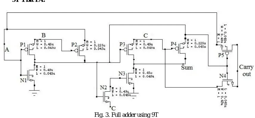
Fig. 3. Full adder using 9T
The circuit shown in Fig. 3 is the 9T FA which is the modified version of 8T FA using an extra transistor N2 that improves the performance of the FA circuit [1]. In 8T FA when inputs are ABC=000, 010 and 110 then problem persists as two transistors get ON simultaneously at the second stage of EXOR and results into the degradation of Sum output due to reduced device resistance as the ON transistors will have combined parallel effect on resistance. Extra transistor N2 gives solution for this problem. Now with inputs 010 and 100, the first stage XOR gate gives “1” which enables the extra added NMOS N2 giving complete “0”. This FA doesn’t give full swing output, so proposed FA removes this full swing problem and provides lower delay for the Sum and Carry out. 9T FA also dissipates more power which dissipates from the input sources.
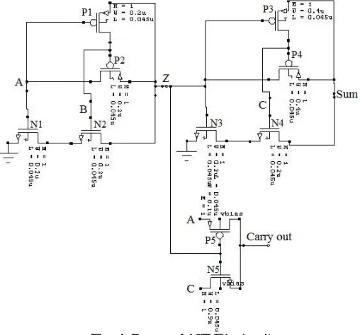
III. PROPOSED 10T FULL ADDER
Here, we are going to describe proposed 10T FA circuit which has lowest delay for sum and carry out generation when input is applied. Transistors N1, N2, P1 and P2 work as EXOR gate [4] means when both the input A and B are same, then
A B Cin Sum Carry out
0 0 0 0 0
0 0 1 1 0
0 1 0 1 0
0 1 1 0 1
1 0 0 1 0
1 0 1 0 1
1 1 0 0 1
ISSN(Online): 2320-9801
ISSN (Print): 2320-9798
I
nternational
J
ournal of
I
nnovative
R
esearch in
C
omputer
and
C
ommunication
E
ngineering
(An ISO 3297: 2007 Certified Organization)
Vol. 3, Issue 8, August 2015
its output is “0” and when both inputs are opposite, then its output is “1”. Intermediate node Z is simply the sum of input A and B. And transistors N3, N4, P3 and P4 are also act as EXOR gate for the input Z and C. So output Sum is the EXOR operation of A, B and C inputs. Carry out depends on the Z (A EXOR B) and inputs A & C. It is implemented using 2T multiplexer design. This design gives very low delay for the Sum output and Carry out. Carry out delay is reduced by using negative bias at the body terminal of the transistor P5 and N5 that makes these transistors so fast for the required operation. This negative bias lowers the threshold of transistors P5 and N5. Carry out delay should be lower for the more than 1-bit adder circuits. The proposed adder design is useful for the 1-bit, 2-bit, 4-bit, 8-bit and 16-bit adder circuits and gives lower power dissipation and fast speed performance. Here, we didn’t use power supply (vdd) but input sources supply the required power for the operation of adder. Carry out doesn’t have full swing for some combination which are shown in Fig. 5.
Fig. 4. Proposed 10T FA circuit
IV. SIMULATION RESULTS
ISSN(Online): 2320-9801
ISSN (Print): 2320-9798
I
nternational
J
ournal of
I
nnovative
R
esearch in
C
omputer
and
C
ommunication
E
ngineering
(An ISO 3297: 2007 Certified Organization)
Vol. 3, Issue 8, August 2015
Fig. 5. Simulation waveform of proposed 10T FA circuit
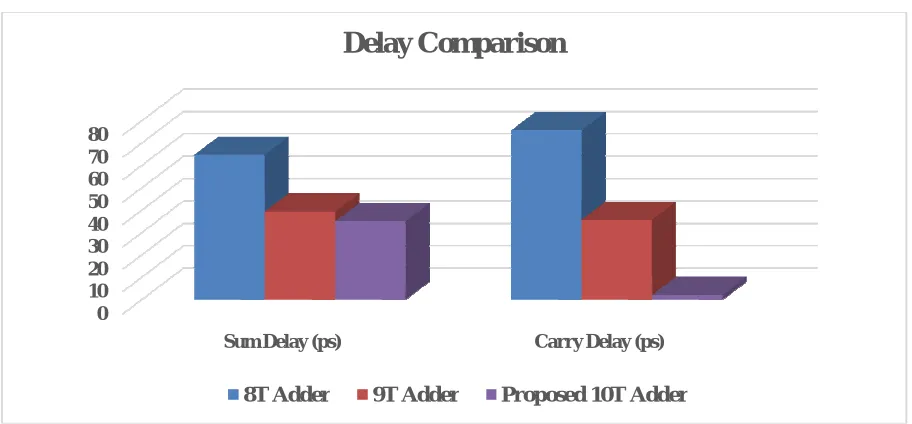
TABLE I. Delay Comparison of different Full Adders
0 10 20 30 40 50 60 70 80
Sum Delay (ps) Carry Delay (ps)
Delay Comparison
8T Adder 9T Adder Proposed 10T Adder
Adders Sum Delay (ps) Carry Delay (ps)
8T Adder [1][2] 64.81 75.83
9T Adder [1] 39.49 35.74
ISSN(Online): 2320-9801
ISSN (Print): 2320-9798
I
nternational
J
ournal of
I
nnovative
R
esearch in
C
omputer
and
C
ommunication
E
ngineering
(An ISO 3297: 2007 Certified Organization)
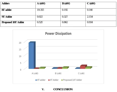
Vol. 3, Issue 8, August 2015 TABLE 2. Power dissipation Comparison of different Full Adders
Adders A (uW) B (uW) C (uW) 8T adder 19.355 0.192 0.166
9T Adder 0.023 0.327 2.154
Proposed 10T Adder 0.529 0.862 0.934
V. CONCLUSION
In this paper, we have proposed a high performance low power 10T full adder which gives better performance than other FAs. It shows lowest delay and power dissipation. It gets almost full swing for Sum and Carry out (for particular combinations) during operations. 10T FA gives 10.93% lower delay than 9T FA circuit and 45.50% lower delay than 8T FA circuit. Proposed 10T FA is beneficial for the higher bit adders and it can be used for any arithmetic operations.
REFERENCES
[1] D. Sinha, T. Sharma, K.G. Sharma, B.P. Singh, “Ultra Low Power 1-Bit Full Adder,” International Symposium on Devices MEMS, Intelligent Systems & Communication (ISDMISC), 2011.
[2] T. Sharma, K.G. Sharma, B.P. Singh, “High Performance Full Adder Cell: A Comparative Analysis” IEEE Student’s Technology Symposium,IIT Kharagpur, April 2010.
[3] H.Eriksson, P. L.Edefors, T. Henriksson, C. Svensson, “Full-custom vs. standard-cell design flow: an adder case study,” In Proceedings of the Asia and South Pacific Design Automation Conference, pp.507-510, 2003
[4] J. Wang, S. Fang, and W. Fang, “New efficient designs for XOR and XNOR functions on the transistor level,” IEEE J. Solid-State Circuits, vol. 29, no. 7, pp. 780–786, Jul. 1994
[5] Chowdhury, S. R. Banerjee, A. Roy, A. Saha, H, “A high speed 8 transistor full adder design using novel 3 transistor XOR gates in International Journal of Electronics, Circuits and Systems 2, 217
[6] T.Vigneswaran, B. Mukundhan, and P. Subbarami Reddy, “A novel low power, high speed 14 transistor CMOS full adder cell with 50% improvement in threshold loss problem,” World Academy of Science,Engineering and Technology 13 2006.
[7] T.Vigneswaran, B. Mukundhan, and P. Subbarami Reddy, “A novel low power and high speed performance 14 transistor CMOS full adder cell,” Journal of Applied Sciences, vol. 6, no. 9, pp. 1978-1981, 2006.
0 5 10 15 20
A (uW) B (uW) C (uW)
Power Dissipation
ISSN(Online): 2320-9801
ISSN (Print): 2320-9798
I
nternational
J
ournal of
I
nnovative
R
esearch in
C
omputer
and
C
ommunication
E
ngineering
(An ISO 3297: 2007 Certified Organization)
Vol. 3, Issue 8, August 2015
[8] H. T. Bui, Y. Wang, and Y. Jiang, “Design and analysis of low-power 10- transistor full adders using XOR-XNOR gates,” IEEE Trans. Circuits Syst.II, Analog Digit. Signal Process, vol. 49, no. 1, pp. 25–30, Jan. 2002.
[9] T.Sharma, K.G.Sharma, B.P.Singh, N.Arora, “High Speed, Low Power 8T Full Adder Cell with 45% Improvement in Threshold Loss Problem,” Proceedings of the 12th International Conference on Networking, VLSI andSignal Processing, p. 272, Coimbatore and University of Cambridge, UK, Feb. 2010.
[10] N. Weste and K. Eshraghian, Principles of CMOS VLSI Design, A System Perspective. Reading, MA: Addison-Wesley, 1993.
[11] R. Shalem, E. John, and L. K. John, “A novel low power energy recovery full adder cell,” in Prod. IEEE Great Lakes VLSI symp. , pp. 380-383, Feb. 1999.