ABSTRACT
KOTIPALLI, VENKATA SATYA VINODH. Impact of Process Variations on 16-nm Dual-Floating Gate FET using TCAD Simulations. (Under the direction of Dr. Paul Franzon).
The inherent uncertainty in processing conditions during the semiconductor fabrication is called process variation. These process variations cause fluctuations in the structural attributes (like oxide thickness, doping concentrations, etc) of the fabricated devices on the chip, due to which the corresponding electrical characteristics of these devices also fluctuate. A robust chip design methodology is required to include the effects of process variations at device design stage itself. Therefore, this thesis explores the impact of process variations on the threshold voltage characteristics of newly proposed dual-floating gate field effect transistor (DFGFET) while studying its application as a unified memory device.
Digital memory can be divided broadly into volatile and non-volatile memory based on retention of the stored data. Volatile memories like SRAM, DRAM require the power supply to be ON for retaining the stored data, i.e. data stored in the volatile memory is lost once the power supply is OFF. While non-volatile memories like Flash, FeRAM, PCM retain the stored data even when power is OFF. The silicon-on-insulator (SOI) based dual-floating gate device discussed in this work could operate in both volatile and non-volatile memory modes, and thus it can be used as a volatile memory or a non-volatile memory or a unified volatile/non-volatile memory.
voltage is not sufficiently high, charges on floating gates are just redistributed and then quickly return to original state once the voltage is removed. On applying a higher voltage, charges ‘tunnel’ from channel to the floating gates, and are retained for a longer time even after the voltage is removed. In other words, a low voltage pulse corresponds to volatile memory operation and a high voltage pulse corresponds to non-volatile memory operation. Potentially a DFGFET can store 2-bit information corresponding to four possible memory states, each with a unique threshold voltage value.
Impact of Process Variations on 16-nm Dual-Floating Gate FET using TCAD Simulations
by
Venkata Satya Vinodh Kotipalli
A thesis submitted to the Graduate Faculty of North Carolina State University
in partial fulfillment of the requirements for the degree of
Master of Science
Electrical Engineering
Raleigh, North Carolina 2013
APPROVED BY:
_______________________________ ______________________________
Dr. Paul Franzon Dr. Veena Misra
Chair of Advisory Committee
DEDICATION
BIOGRAPHY
ACKNOWLEDGMENTS
I would like to thank several people that have supported and assisted me throughout my graduate work. First of all, I would like to thank my advisor Dr. Paul Franzon for providing me with the opportunity to gain knowledge by working on advanced research topics and for his guidance and feedback along course my research. I would like to thank Dr. Veena Misra and Dr. Neil Di Spigna for being on my thesis committee and supporting me in my research. Specially, I would like to thank Dr. Neil for his help in setting up initial
simulations and in designing the 2nd generation Unified Memory Masks. I also like to thank Narayanan Ramanan for his help in addressing issues related to Sentaurus-TCAD
TABLE OF CONTENTS
LIST OF TABLES ... vii
LIST OF FIGURES ... x
Chapter 1: Introduction ... 1
1.1 Motivation ... 1
1.2 Thesis Outline ... 3
Chapter 2: Literature Review ... 5
2.1 Overview of Semiconductor Memory ... 5
2.2 Volatile Memory ... 7
2.2.1 SRAM ... 8
2.2.2 DRAM... 10
2.3 Non-Volatile Memory ... 13
2.3.1 Operation Principle of Flash Memory ... 15
2.3.2 NOR Flash Memory ... 18
2.3.3 NAND Flash Memory... 19
2.4 Dual-Floating Gate Unified Memory Device... 20
2.4.1 Dynamic or Volatile memory mode ... 23
2.4.2 Non-Volatile memory mode ... 24
2.4.3 Applications of the Dual-Floating Gate Device ... 26
2.4.4 Design challenges and possible solutions ... 28
2.5 Impact of Process Variations... 30
Chapter 3: Impact of Macro and Micro Level Process Variation... 31
3.1 Tunneling mechanisms ... 31
3.1.1 Direct Tunneling ... 32
3.1.2 Fowler-Nordheim Tunneling ... 34
3.1.3 Tunneling models in Sentaurus-TCAD ... 35
3.2.1 SOTB based dual-floating gate device ... 37
3.2.2 Simulation results... 40
3.3 Micro-level variations ... 48
3.3.1 Simulation of Random Dopant Fluctuation (RDF) ... 49
3.3.2 RDF Vs Channel doping concentration ... 51
3.3.3 Dual-floating gate Device with undoped channel ... 52
3.3.4 Impact of RDF on Dynamic Refresh Rate ... 56
Chapter 4: Precise-Write Approach ... 58
4.1 Precise-Write algorithm ... 58
4.2 Simulation Results... 60
Chapter 5: Design Optimization of the dual-floating gate structure ... 67
5.1 Dual-floating gate device with lower work function top floating gate ... 67
5.2 Impact of process variations on the optimized DFGFET structure ... 71
5.2.1 Impact of macro-level variations ... 73
5.2.2 Impact of RDF ... 75
5.2.3 Impact of process variations on Dynamic Refresh Rate ... 76
5.2.4 Dynamic Refresh Rate improvement with Precise-Write Approach ... 78
Chapter 6: Conclusion and Future Work ... 81
6.1 Conclusion ... 81
6.2 Future Work ... 83
REFERENCES ... 85
APPENDIX ... 91
LIST OF TABLES
Table 2.1 Comparison between different non-volatile memory technologies [2]. ... 14
Table 3.1 Design specifications of SOTB based DFGFET ... 38
Table 3.2 List of sources for macro variations with respective uniformity values ... 43
Table 3.3 Impact of macro variations on threshold voltages for all the 4-states ... 44
Table 3.4 Impact of macro variations on threshold voltage shift for all the 4-states, when read operation uses only one reference cell (S00). ... 46
Table 3.5 Impact of macro variations on threshold voltage shift for all the 4-states, when read operation uses two reference cells (S00 & S10) ... 47
Table 3.6 Impact of Random Dopant Fluctuations on VTh and Δ2VTh for all the 4-states 50 Table 3.7 Impact of Random Dopant Fluctuations on VTh and Δ2VTh for different channel doping concentration (NSOI) values ... 51
Table 3.8 Impact of Random Dopant Fluctuations on SOTB based dual-floating gate structure (Figure 3.3) with undoped channel. ... 53
Table 3.9 Simulation results of Undoped DFGFET showing the threshold voltage for all the 4-states along with the corresponding macro-level variations in Δ2VTh values. ... 55
Table 3.10 Impact of Random Dopant Fluctuations on SOTB based dual-floating gate structure (Figure 3.7) with undoped channel and source/drain underlap. ... 56
Table 4.2 Simulation results of the precise-write algorithm based dynamic programming for state S01, attempt #2 (Only RDF is included). ... 62 Table 4.3 Simulation results of the precise-write algorithm based dynamic programming
for state S01, attempt #3 (Only RDF is included). ... 63 Table 4.4 Simulation results of the precise-write algorithm based dynamic programming
for state S01, attempt #4 (Only RDF is included). ... 64 Table 4.5 Simulation results of the precise-write algorithm based dynamic programming
for state S11 (Only RDF is included). ... 66 Table 5.1 Design specifications of the DFGFET with different top floating gate metals. 68 Table 5.2 Summary of simulation results corresponding to the DFGFET design
specification listed in Table 5.1 ... 69 Table 5.3 Design specifications of the optimized dual-floating gate device. ... 72 Table 5.4 Simulation results of optimized DFGFET showing the impact of macro-level
variations on dynamic programming and dynamic retention ... 73 Table 5.5 Corner conditions resulting in lowest dynamic retention Δ2VTh values. ... 75 Table 5.6 Impact of Random Dopant Fluctuations on optimized dual-floating gate device
structure (Figure 5.2) with nominal design specifications ... 75 Table 5.7 Impact of Random Dopant Fluctuations on dynamic mode operation of the
DFGFET device with corner case design specifications listed in Table 5.5 .... 76 Table 5.8 Simulation results of the precise-write algorithm based dynamic programming
LIST OF FIGURES
Figure 2.1 Schematic circuit diagram of 6T-SRAM bit cell ... 8 Figure 2.2 Schematic circuit diagram of 1T-DRAM bit cell ... 11 Figure 2.3 Cross-section of floating gate device, the basic element of a Flash memory ... 15 Figure 2.4 Flash memory showing a) CHEI based programming operation and b)
Fowler-Nordheim tunneling based high-voltage source erase operation ... 17 Figure 2.5 Schematic circuit diagram showing a column in NOR Flash memory array ... 18 Figure 2.6 Schematic circuit diagram showing a column of NAND Flash memory array 20 Figure 2.7 Cross-section and doping profile of 16-nm dual-floating gate device [1] ... 21 Figure 2.8 Band diagram across the gate stack of DFGFET under flat band condition[2] 22 Figure 3.1 Band diagram of an arbitrary metal-insulator-metal (MIM) structure showing
direct tunneling (DT). ... 32 Figure 3.2 Band diagram of an arbitrary metal-insulator-metal (MIM) structure
Fowler-Nordheim tunneling (FNT) ... 34 Figure 3.3 A simplified cross-section of 16 nm dual-floating gate device on lightly doped
SOI substrate (1x1015 cm-3) with a heavily doped p-type silicon backgate. ... 37 Figure 3.4 Schematic cross-section of SOTB NMOS with 65-nm gate length [31] ... 39 Figure 3.5 Id-Vg curves for all the four states of SOTB based dual-floating gate device . 41 Figure 3.6 Plot of RDF based standard deviations in VTh and Δ2VTh as a function of
Figure 3.7 A simplified cross-section of 16 nm dual-floating gate device with undoped channel and source/drain underlap. ... 54 Figure 3.8 Plot of number of errors per million due to RDF corresponding to states S01
and S11 as a function of refresh time(TR) ... 57 Figure 4.1 Flow chart showing the precise-write algorithm ... 59 Figure 5.1 Standard deviations in Δ2VTh for Devices A to E due to variations in a) inter
floating gate oxide thickness (tox2) and b) tunneling oxide thickness (tox2) ... 70 Figure 5.2 A simplified cross-section of 16 nm dual-floating gate device with undoped
channel and source/drain underlap which is designed to minimize the macro-level variations (Device-E) ... 71 Figure 5.3 Simulation results of corner conditions for tSOI and tBOX, with tox1 = 41.2 ,
tox2 = 56.0 , tox3 = 171.7 , NSUB = 5x1018 cm-3 & NS/D = 7x1019 cm-3. ... 74 Figure 5.4 Plot of number of errors per million due to process variations corresponding to
Chapter 1: Introduction
This chapter starts with the motivation behind the current work on simulating the impact of process variations on the threshold voltage characteristics of a 16-nm unified memory device, followed by a brief outline of thesis organization.
1.1
Motivation
In 2011, Schinke et al. reported the design, operation and architectural implications of novel dual-floating gate device for applications like unified (non-volatile + volatile) memory, instant-on computing, “just in time” (JIT) network switches etc [1]. Using dual-floating gate device for these applications involve several design issues and trade-offs, some of them were discussed in D. Schinke’s dissertation [2]. Dual-floating gate field effect transistor
non-volatile memory operation and a low voltage pulse corresponds to non-volatile memory operation. The trapped charges in the floating gates produce a shift the threshold voltage of the device, which is used to identify different volatile and volatile memory states of the dual-floating gate device. Using DFGFET for creating unified non-volatile/volatile main memory offers several advantages over the traditional DRAM [2]. The fabrication costs would be lower due to the absence of the storage capacitor. Additionally, the density of the memory array is also expected to be higher due to better scalability, especially when fabricated on Silicon-On-Insulator (SOI) platform. The dynamic retention of the DFGFET is expected to be much longer than the conventional DRAM, because of which even with the higher programming voltages the overall power consumption would be lower than DRAM. Moreover, whenever required the data stored in volatile mode can be quickly transferred to energy efficient non-volatile mode within few cycles. Thus, overall power efficiency of the memory system can be further improved by partial or complete hibernation unused parts of the memory, where the hibernation is carried out by copying the data from volatile mode to non-volatile mode. The simulated results of 16-nm DFGFET based unified memory device were reported along with the measured threshold voltage shifts of 100-µm fabricated dual-floating gate MOSCAPs [1-2].
The primary focus of D. Schinke’s dissertation is to demonstrate the concept of
variations. The process variations in the dual-floating gate device have to be included at device design phase itself, and design has to be optimized to minimize the impact of these variations on the threshold voltage characteristics of the device. This is precisely the problem addressed in this thesis and the proposed solutions involve both device level techniques and circuit level techniques. Device level techniques comprise use of undoped-channel, source/drain overlap and thicker inter floating gate dielectric. Circuit level techniques include dual-reference reading and iterative dynamic writing (or precise-write). Device level simulations using Sentaurus-TCAD is used to evaluate these design solutions. The discussion of circuit level techniques is limited to providing the required sense amplifier specifications for reducing the impact of process variations. However, the detailed sense amplifier circuit design is not included in the scope of this thesis.
1.2
Thesis Outline
The literature review in chapter 2 gives an overview of different volatile and non-volatile memory technologies, followed by application of silicon-on-insulator (SOI) based dual-floating field effect transistor (DFGFET) as a unified memory device. The basic structure of the dual-floating gate device, operational principle, applications and design challenges are discussed in detail.
Chapter 4 explores the iterative dynamic programming approach for improving the dynamic refresh rate by compensating the impact of random dopant fluctuations. The details of this approach are discussed, and the simulation results of programming voltage sequences to achieve 6-sigma BER with longer refresh times are presented.
Chapter 5 presents the optimal design for dual-floating gate device for reducing the impact of macro-level variations. The impact of all the process variations on this optimal design is investigated using the TCAD-simulations and the corresponding minimum refresh period requirement (with and without the precise-write algorithm) to maintain the 6-sigma level BER is also evaluated.
Chapter 2: Literature Review
This chapter gives an overview of different volatile and non-volatile memory
technologies, followed by application of silicon-on-insulator (SOI) based dual-floating field effect transistor (DFGFET) as a unified memory device. The basic structure of the dual-floating gate device, its operational principle and its applications are presented in detail. In the final part of this chapter, some of the design trade-offs reported in the literature are discussed followed by a brief discussion the importance of estimating the process variations during the device design process.
2.1
Overview of Semiconductor Memory
The term memory in an electronic system usually refers to the hardware designed to store data, which can be accessed as per the requirements of rest of the system. In general an electronic system has a processor, an operating system (OS) and a memory block to support the software as well as to handle the data flow in and out of the processor. Typically semiconductor based memory circuits are used due to their fast access speeds. Memory makes up roughly 20-25% of the global semiconductor market [29]. Also, the current market size of semiconductor memory is around 60 billion US dollars, and it is expected grow over 90 billion US dollars by 2017.
the systems multi-level lower capacity on-chip memory called cache is used along with higher capacity external memory chip called main-memory. Being on the same chip, cache has much quicker access speeds compared to main-memory. Even larger capacity semiconductor memory units like flash drives and SSDs are used to store data in more permanent basis. Therefore, depending on the system requirements different memory technologies could be used for memory components.
The fundamental building block of a semiconductor memory is a bit cell, which is a tiny circuit to store a single bit of binary data. The size of a memory cell could just be a single transistor or more than one transistor, depending on the memory technology. Updating the value stored in a memory cell is called the “write” process and probing the memory cell to determine the value stored in it is called the “read” process. The read and write speeds
vary with the type of memory technology used. These memory cells are arranged in a rectangular array, and the size of an array determines the capacity or size of the memory chip. Typically memory cells are accessed using word address with each address representing a unique set of bit cells called a word. The size of a word or word-length could be any power of two, but it is commonly equal to or greater than eight. The key advantage of semiconductor memory is that all the locations in the memory array can be accessed in the same amount of time, and the stored data can be accessed efficiently in any random sequence. This property is known as random access, and it greatly simplifies the memory allocation process.
Especially the advances in portable devices like smart phones and tablets demand for memory technologies that are compact, fast and power-efficient, all three at the same time. A lot of research is carried out in developing newer semiconductor memories that could support the needs for future technology nodes. Based on whether the stored data is retained or not when the power supply is OFF, semiconductor memory technologies can be broadly categorized into two groups, namely volatile memory and non-volatile memory. Typically non-volatile memories are more power efficient but are slower than the volatile memories. The following sections give a brief overview of both volatile and non-volatile memory along with some examples, and introduce the dual-floating gate unified memory device.
2.2
Volatile Memory
2.2.1
SRAM
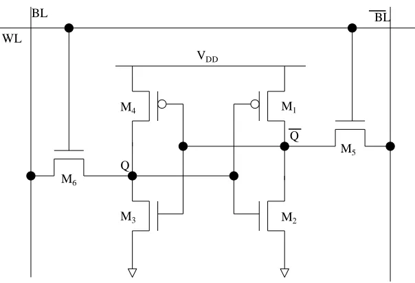
Figure 2.1Schematic circuit diagram of 6T-SRAM bit cell
Static random-access memory (SRAM) is a high-speed, power efficient volatile semiconductor memory that stores data using two cross-coupled inverters (M1–M4) which
form a bi-stable latching circuit. A typical 6T-SRAM bit cell has a total of 4 NMOS and 2 PMOS transistors as shown in Figure 2.1. Each bit cell can be activated for reading or writing operations by the word-line (WL), which controls the gate terminals of two NMOS transistors M5 and M6. The bit-lines (BL & ) are used to access data in and out of an active bit cell. In a SRAM memory array, each set of bit-lines (BL & ) is connected to several cells arranged in a column, and each word-line (WL) is connected to several
bit-M1
M2
M3
M4
M5
M6
BL BL
WL
VDD
Q
cells arranged in a row. Each of these word-lines represents a unique memory address with word-length equal to the number of bit-cells a single row.
Fundamentally, a SRAM cell is expected to be in one of three operating modes standby, reading or writing. Standby mode is the one in which data stored in the SRAM cell is maintained constant as long as the power supply (VDD) is ON. This standby mode is maintained when the word-line (WL) is low, which isolates the bit-cell by keeping the access transistors M5 and M6 in OFF state.
Reading mode is the one in which the data stored in the SRAM cell is accessed to determine if the value is 0 or 1. In the first half of the read cycle, both the bit-lines (BL &
) are precharged to logic-1 and in the second half, both the access transistors are turned
ON by setting word-line (WL) high. During the second half of the read cycle, one of the bit-lines is pulled down by the cross coupled inverters leaving the other line at the precharged value, thereby reflecting the stored value (Q & ) on to the bit-lines (BL & ). If Q is logic-1 will be discharged and if Q is logic-0 BL will be discharged. Modern day SRAM circuits have sense amplifiers to detect the voltage difference between the lines BL & and determine if the stored data is logic-1 or 0. Sense amplifiers with higher sensitivity require relatively smaller voltage difference to identify logic-1 from logic-0, which enables them to complete the read operation quicker.
The transistors M5 and M6 are sized such that, when one of the bit-lines (BL or ) is low during writing they can overpower the pull-up transistors M1 & M4. The pull down transistors M2 and M3 are sized for overpowering the access transistors M5 & M6 during read operations. SRAMs are faster and power-efficient, but are less dense compared to DRAM counterparts; so they cost higher. Typically SRAMs are used in applications that require high bandwidth and/or low power, like cache memory (L1, L2 etc) in central processing unit (CPU).
2.2.2
DRAM
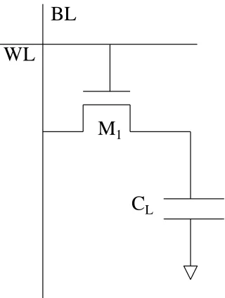
Figure 2.2Schematic circuit diagram of 1T-DRAM bit cell
Similar to SRAM, DRAM cell also operates in one of the three modes - standby, read and write. Standby in DRAM can be considered to be the one in which the word-line (WL) is maintained low so that the pass-transistor M1 remains disconnected. The disadvantage of a DRAM is that even in the standby mode, the stored data is gradually lost due to capacitive leakages.
Writing mode is the one in which data stored in the DRAM cell is updated with new values. Write cycle begins by loading the new data on to bit-line (BL) i.e. to write logic-1 BL is charged to VDD and to write logic-0 BL is discharged to ground. Then the word-line is set high for charging or discharging the storage-capacitor (CL) according to the voltage on the bit-line (BL).
M
1C
LBL
The first half of the DRAM read cycle has word-line (WL) set to low and bit-line (BL) is pre-charged to pre-set reference voltage with a value below VDD. As the bit-line (BL) is pretty long and connects multiple bit-cells in a column, they carry a considerable amount of capacitive load. Thus, the precharged voltage on the bit-line (BL) will be maintained for a short period of time even after disconnecting the precharge circuit. During the second half of the read cycle, the precharge circuit is disconnected and pass transistor M1 is activated by raising the word-line (WL) to high. Once the pass-transistor is active, charge gets transferred between the storage-capacitor (CL) and the connecting bit-line (BL). If the stored value in the bit cell is logic-0, then the bit-line voltage decreases considerably; as most of the precharged charge on bit-line (BL) is used to charge the storage-capacitor (CL). If the stored value in the bit cell is logic-1, then the decrease in bit-line voltage is very little; as only a small portion of the precharged charge on bit-line (BL) is enough for charge leveling. Sense amplifiers are used to detect the change in voltage of the bit-line (BL) and determine the data stored in the bit-cell [13]. In contrast to SRAM, reading process in DRAM is not non-destructive; therefore stored charge in the capacitor CL gets corrupted after each read. Thus, output of the sense amplifier is used to reload the original data on to the bit-cell.
differ from system to system, i.e. refresh cycles of all the rows in a DRAM chip can be either be clubbed together or could be spread out with equal intervals to achieve an overall refresh rate of 64 ms.
One critical issue for DRAM scaling is that smaller sized capacitors store lesser charge, which puts more pressure on sense amplifiers to detect much smaller change in voltages. This could increase the bit-error rate and/or make it difficult to meet the required specification of 64 ms refresh rate.
Compared to SRAMs, DRAMs have longer write times (few 10s nanoseconds) and higher power consumption because of dynamic logic and the refresh requirements. However, they have pretty high density, which reduces the cost per bit significantly. In general, DRAMs are used in applications that require high storage capacity, like main memory in central processing unit (CPU).
2.3
Non-Volatile Memory
plates, whose resistance could be modified by changing the relative polarities of two plates. PCM uses a phase changing film of chalcogenide material that transforms between amorphous and crystalline phases reversibly depending on the applied heat, which leads to change in the resistance values. The NAND and NOR Flash technologies [3,8] use storage element similar to MOSFET except for the fact that it has a floating gate between the control gate and the semiconductor. This floating gate is used to trap charges by tunneling, which thereby produce a shift in threshold voltage.
Table 2.1 Comparison between different non-volatile memory technologies [2]. Attribute NOR Flash
[3,8] NAND Flash [3] FeRAM [3,4,5,6,8,9] MRAM [3,8,11] PCM [3,7,8,10]
Cell Size 10F2 4-5F2 15-100F2 10-30F2 8-20F2
Endurance 105-6 cycles 105-6 cycles 108-12 cycles 109-16 cycles
109-12 cycles Program Time 1 µs 200 µs/page 30-200 ns 10-30 ns 10-100 ns Erase Time 1 s/sector 2 ms/block 30-200 ns 30 ns 100-120 ns Read Time 20-60 ns 60 ns/serial 20-80 ns 10-30 ns 20-100 ns
Scalability Fair Fair Poor Poor Good
Multi-Bit Possible Possible No No Difficult
Cost/Bit Medium Low High High Medium
Maturity High High Medium Medium Medium
Fabrication Process Full Custom or +10 masks Full Custom or +10 masks
+ 2-3 masks back-end
process
+4-6 masks back-end
process
+ 2-3 masks back-end
Flash memory is the dominant non-volatile memory technologies with fastest market growth for two main reasons: (i) Its ready compatibility to CMOS fabrication process and (ii) its high maturity of technology development. The relative comparison of these non-volatile technologies is shown in Table 2.1; as it can be seen the NAND and NOR Flash are more matured than rest of the technologies. Also, Flash memory technology has more relevance to unified memory device discussed in this thesis. Therefore, the basic structure and operational principal of Flash memory is discussed in the remaining part of this subsection
2.3.1
Operation Principle of Flash Memory
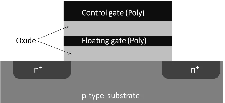
Figure 2.3Cross-section of floating gate device, the basic element of a Flash memory
n
+n
+Floating gate (Poly)
Control gate (Poly)
Oxide
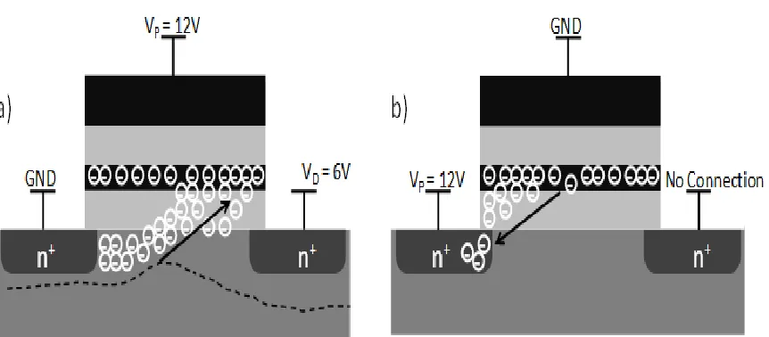
The structure of the basic building block of Flash memory, a typical floating gate (FET) is shown in Figure 2.3. The electrode on top of the gate stack is the control gate, and the other electrode is the floating gate. The oxide separating floating gate and the p-type silicon substrate is called tunneling oxide. The oxide separating floating gate and the control gate is called control gate oxide or blocking oxide. Floating gate acts as the charge storage node; value of the charge on it is controlled by applying appropriate voltage pulses on control gate, source and drain. Each of this floating gate device forms a single Flash memory cell. A collective array of these cells forms a highly dense Flash memory unit. A typical Flash memory array can be connected either in NAND or NOR configuration.
voltage, control gate is grounded and drain is left unconnected. The relatively large positive voltage on source attracts the negative charge on the floating gate to source through the tunneling oxide. This particular erase operation is called high-voltage source erase [26].
As described earlier a programmed device (VTh2) has a higher threshold voltage than the erased device (VTh1), i.e. VTh2 > VTh1. Read operation is carried out by applying read-voltage on control gate with value between the two threshold read-voltages (VTh1 & VTh2). If the device is in programmed state (logic-0) the cell will be in OFF state, and if the device is in erased state (logic-1) the cell will be in ON state. Thus, data stored in Flash memory is read by sensing if the memory cell is conductive or not.
Compared to volatile memories like DRAM and SRAM, Flash memory has significantly large writing time (ref. Table 2.1) and high program/erase voltages. Another limitation of Flash memory is that though the programming and reading can be carried out at word or byte level; the erase process can only be carried out at the block level. On the positive side, Flash memory has remarkably low power consumption, high memory density and retains the stored data even when the power supply is OFF. Generally, Flash memory is used in secondary storage devices like flash drives, solid state drives (SSD), etc.
2.3.2
NOR Flash Memory
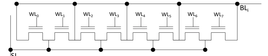
Figure 2.5Schematic circuit diagram showing a column in NOR Flash memory array
The rotated version of a column in a typical NOR Flash is shown in Figure 2.5, several of these columns each with a unique bit-line (BLi, where i=0,1,2.. etc) make a memory array. Same word-lines (WL0,WL1 .. etc) are used to access all the corresponding memory cells in each of the column, i.e. same word-line is used to access all the memory cells in the single row. The source nodes of all the memory cells in the array are connected
WL0 WL1 WL2 WL3 WL4 WL5 WL6 WL7
BLi
together using a common source-line (SL). Instead of having single large memory array, the memory chip is hierarchically divided into multi-level sub-arrays namely pages, sectors and blocks. Programming in a NOR Flash is carried using hot electron injection, and erase is done Fowler-Nordheim tunneling (FNT). The F-N erase is not limited to the high-source voltage erase; instead it can also be negative gate source erase or channel erase [26]. The most significant advantage of NOR Flash is their higher reading speeds, but program and erase speeds are slower than that of NAND Flash. Also, addressing NOR Flash for read operation is similar to that in any random-access memory. Thus, NOR Flash are popular in execute in place (XIP) applications that boot or execute code directly from Flash, where the critical function is read operation.
2.3.3
NAND Flash Memory
span or endurance of NAND Flash larger than that of NOR Flash. Thus, NAND Flash is the best suited for secondary memory storage applications like flash drives and SSDs.
Figure 2.6Schematic circuit diagram showing a column of NAND Flash memory array
2.4
Dual-Floating Gate Unified Memory Device
The cross-section of SOI-based 16-nm dual-floating gate device (DFGFET) with backgate reported by Schinke et al. [1] is shown in Figure 2.7, and the band diagram across its gate stack is shown in Figure 2.8. This DFGFET structure is similar to a MOSFET except for the fact that it has two metal floating gates stacked between the control gate and the silicon substrate. These floating gates are used to trap charges by tunneling, which thereby produce a shift in threshold voltage (ΔVTh). The polarity of floating gate charges determines if the threshold voltage increases or decreases with respect to the uncharged device. Ability
WL0 WL1 WL2 WL3 WL4 WL5 WL6 WL7 SSL
GSL
BLi
Figure 2.7Cross-section and doping profile of 16-nm dual-floating gate device [1]
to function as a unified memory that can operate simultaneously in both faster volatile memory mode and power efficient non-volatile memory mode brings novelty to this dual-floating gate structure
oxide (OX2), which is made of HfSiO and has a thickness of 3.2 nm. The dielectric barrier separating the top floating gate and the control gate is called top oxide or control gate oxide or blocking oxide (OX3), which is made of HfO2 and has a thickness of 18 nm. The dielectric barrier separating the backgate and the SOI substrate is called backgate oxide (OXBG), which is made of SiO2 and has a thickness of 1.2 nm. As far as doping profiles are concerned, p-type SOI substrate is uniformly doped boron (B) at a concentration of 5.0x1015 cm-3 and source/drain regions are highly doped with n-type arsenic atoms at a concentration of 7.0x1019 cm-3.
Figure 2.8Band diagram across the gate stack of DFGFET under flat band condition[2]
1
.2
0
e
V
4
.6
0
eV
2.4.1
Dynamic or Volatile memory mode
To program the dual-floating gate device, a positive voltage bias is applied across the gate stack, i.e. voltage on control gate is greater than backgate (VCG > VBG). For the device to operate in dynamic mode, the applied voltage should be high enough to facilitate tunneling between the floating gates but should not be high enough to support tunneling of electrons from channel to floating gates. The tunneling through inter floating gate oxide leads to rapid charge redistribution between the two floating gates, resulting in equal and oppositely charged floating gate. Since positive voltage is applied on control gate, the top gate becomes negatively charges and bottom gate becomes positively charged. Bottom floating gate is closer to channel than the top floating gate, hence has a stronger influence on the I-V characteristics of the device. This positively charged bottom floating gate produces a negative threshold voltage shift (~ -330 mV) with respect to uncharged device [2]. Thus, the dynamic state of the DFGFET can be sensed by measuring the change in threshold voltage.
These accumulated charges on the floating gates are retained even after the applied voltage is removed, but they get discharged by tunneling back across the inter floating gate oxide. This means that the stored data gets corrupted due to leakage and requires to be continuously refreshed similar to DRAM. Thus, this device is considered to be in volatile or dynamic memory mode. The high work function top floating gate significantly slows down the charge leakage and hence improves the dynamic retention.
takes significantly longer times (10s of µs vs 10s of ns) because of the high energy barrier faced by the electrons while tunneling from top floating gate to bottom floating gate.
Since the voltages used in volatile memory mode are low the corresponding electric fields are also low (<0.2 V/nm). The low energy direct tunneling is the dominant tunneling mechanism under this low electric field conditions, so the damage to the inter floating gate oxide is minimal in this mode. This helps in maintaining a healthy endurance value for the dynamic memory mode [2].
2.4.2
Non-Volatile memory mode
fairly less negatively charged or even slightly positively charges depending on applied voltage envelope. Since the top floating gate is relatively far from channel, only a small positive threshold voltage shift is obtained.
The charges on the floating gates start redistributing after removing the programming voltage, making the bottom floating gate more negative while making the top floating gate less negative. This operation is called non-volatile charge settling, and floating gate charges get saturated once voltage balance on the floating gate pair is achieved. The presence of net negative charge on floating gates puts the device in a deep accumulation mode even if no voltages are applied. This leads to negative surface potential in the range of -0.6 V to -0.7 V [2]. Therefore, top floating gate is required to be more negatively charged than the bottom floating gate for reaching voltage balance on the floating gate pair. The increased negative charge on bottom floating gate after charge settling(~1s after non-volatile programming) produces a larger positive threshold voltage shift(~ +1.52V) with respect to uncharged device[2].
zero. However, immediately after the erase voltage is removed, the top floating gate remains negatively charges where as the bottom floating gate is positively charged. The charge on the floating gates starts redistributing making both floating gates charge neutral (after ~1s) with the process similar to dynamic retention [2]. Thus, the device returns to its uncharged state after the non-volatile erase followed by charge settling.
2.4.3
Applications of the Dual-Floating Gate Device
The key advantage of the dual-floating gate device is that both the volatile memory mode and the non-volatile memory can be handled independently. This means that, each device can actually store 2-bit data, one bit for volatile mode and another bit for non-volatile mode. This 2-bit information can be represented using 4-states namely S00, S01, S10, S11. Where,
S00: Non-volatile mode logic-0 & Volatile mode logic-0 S01: Non-volatile mode logic-0 & Volatile mode logic-1 S10: Non-volatile mode logic-1 & Volatile mode logic-0 S11: Non-volatile mode logic-1 & Volatile mode logic-1
Coexistence of volatile and non-volatile memory modes in a single device supports several energy efficient memory implementations while maintaining volatile memory speeds comparable to DRAM.
data in volatile memory mode on to non-volatile memory during hibernation. In principle, memory array with several memory banks each having 1024 rows could be changed to hibernate-mode in 30 ms because all the memory banks change state in parallel.
Energy efficiency can be further improved by hibernating parts of the memory which are not actively accessed by CPU, i.e. partial hibernation can be used to “freeze” inactive portions of memory so as to avoid power consumption due to dynamic refresh and “unfreeze” them when needed [1].
The non-volatile memory mode of unified memory array can be used to take quick back-up of the volatile mode; this application is called check-pointing. The check-pointing can be taken either in regular intervals or on detection of transient fault or upon power-down. This fast check-pointing significantly improves the computer’s ability to withstand and recover from faults [1], also known as resiliency of the computer.
2.4.4
Design challenges and possible solutions
Several challenges related to using the dual-floating device for unified memory application were discussed by Daniel Schinke in his dissertation[2]. These design challenges along with possible solutions are listed in this subsection.
Endurance requirements: Repeated charging and discharging of floating gates could lead to the formation of defects in the dielectric layers. These defects increase the dielectric leakages and discharge the floating gate charges at much higher rate, resulting in bit error and failure of the device. This is also known as stress induced leakage current (SILC). Thus, number of program and erase cycles before the device failure is called the endurance of device.
Dynamic memory mode of the DFGFET is expected to have high endurance, in order to be comparable to DRAM’s endurance of 1016
cycles. The biggest challenge of unified memory device is to meet this endurance target while sustaining the added stress on inter floating gate oxide during non-volatile programming and erasing. Potential techniques to achieve high quality endurance in additional to the ones normally implemented in Flash memory include the following [2].
Use of direct tunneling in the dynamic memory mode. Direct tunneling is less
Lower voltage and electric fields. Dual-floating gate device uses lower voltage
compared to Flash memory; this again reduces the oxide stresses.
Discontinuous floating gates. Device susceptibility to SILC can be further reduced
by using nanocrystal based discontinuous floating gate pairs instead of continuous floating gates.
Robust dielectrics. Trap-free dielectrics inherently improve the device lifetime.
Tradeoff between Dynamic erase speed and refresh rate: The combination of a high work function top floating gate metal and a low work function bottom floating metal, results in long dynamic retention time, but dynamic erase becomes very slow. On the other hand, faster dynamic erase can be achieved using low work function metals for both top and bottom floating gates; but this would reduce the dynamic retention time significantly. The optimal trade off could be using a physically thicker inter floating gate oxide with a high electron affinity and a narrow band gap along with low work function metal floating gates. This could improve dynamic erase (and program) due to lower barrier height and also maintain longer dynamic retention due to a thicker barrier [2].
2.5
Impact of Process Variations
Large scale production of any semiconductor technology involves several levels of process variations. Same scenario is applicable to fabrication of the dual-floating gate devices as well. No two memory chips or no two devices on the single chip could be perfectly identical due to the presence of finite level of process variations. These process variations get reflected in terms of threshold voltage variations of the unified memory device. A robust chip design methodology has to include these threshold voltage variations at device design stage itself, so as to provide additional safety buffer to meet the device specifications with at least 6-sigma level success rate. A good starting point to estimate the impact of these process variations is to extract the standard deviations in device characteristics using Sentaurus-TCAD based device simulations.
Chapter 3: Impact of Macro and Micro Level Process Variation
This chapter investigates the impact of different macro and micro level process variations on the performance of 16-nm dual-floating gate device based universal memory. Sentaurus-TCAD simulations are performed to estimate the impact of different variation sources independently. Based on these simulation results, possible design modifications that minimize the variations are discussed.
3.1
Tunneling mechanisms
3.1.1
Direct Tunneling
Figure 3.1Band diagram of an arbitrary metal-insulator-metal (MIM) structure showing direct tunneling (DT).
An arbitrary metal-insulator-metal (MIM) structure is used to explain the concept of direct tunneling; however, the concept remains the same even if semiconductors are used instead of metals. The band diagram of this MIM structure in direct tunneling regime is shown in Figure 3.1. A voltage drop of Vins is applied across the thin insulator layer such that
anode is at higher potential than the cathode; this results in an electric field across the insulator in the direction right to left. Due to the applied electric field the electrons get pushed across (or tunneled) the trapezoidal energy barrier. This process of electron tunneling is called direct tunneling.
Φb
E
Cathode
Direct tunneling current is strongly dependent on the thickness of the barrier; it is prominent in ultra-thin insulator layers and low electric fields. The trapezoidal shape of the energy barrier is maintained as long as the condition is met. The current density for direct tunneling is given by the equation [2].
Where,
and,
with,
= effective electron mass in cathode
= effective electron mass in the insulator
q = charge of electron h = plank’s constant and
= height of the barrier
= width of the barrier
= voltage drop across the insulator
3.1.2
Fowler-Nordheim Tunneling
Figure 3.2Band diagram of an arbitrary metal-insulator-metal (MIM) structure Fowler-Nordheim tunneling (FNT)
The band diagram of an arbitrary MIM structure in Fowler Nordheim tunneling regime is shown in Figure 3.2. The energy barrier takes triangular shape when the voltage drop across the insulator is greater than the barrier height. Fowler-Nordheim tunneling exists even with trapezoidal barrier, but becomes the dominant factor in tunneling current at higher electric fields that satisfy the conditions i.e. .
E
Φb qV
ins
Cathode
As mentioned earlier direct tunneling is not significant in thicker insulators, thus F-N would be the biggest contributor to tunneling currents in thick insulators. The current density for F-N tunneling is given by the equation [2]
Where, A and B are constants for a particular material interface, given by
3.1.3
Tunneling models in Sentaurus-TCAD
Tunneling mechanisms incorporated into TCAD simulations by the Sentaurus Device (sdevice) tool. F-N tunneling is the simplest tunneling model handled by sdevice tool, where tunneling current density is modeled using expression given by equation 3.3. The values for A and B instead of being calculated from material properties, they are directly edited in the parameters files for all the relevant material interfaces of interest. This model is activated using one of these statements below [28]
“Physics (MaterialInterface = "Material1/Material2") {GateCurrent (Fowler)}”
“Physics (RegionInterface = "Region1/Region2") {GateCurrent (Fowler)}”
Also, TCAD simulates direct tunneling combined together with Fowler-Nordheim tunneling with a more involved model [28], which is activated using one of these statements
“Physics (MaterialInterface = "Region1/Region2") {GateCurrent (DirectTunneling)}”
3.2
Macro-level variations
Macro-level variations are the process variations that vary more gradually (or systematically) across the wafer or between different wafers of a lot, etc. For example, temperature profile in the furnace used for thermal oxidation (batch process) may vary slightly from one run to another and even in the same run temperature at the ends of furnace may be different from that at the center of the furnace. Even in the single wafer, growth rates may differ across the wafer due to the gas flow patterns of the involved reactants. These individual variations may or may not be significantly high, but several different variation sources when combined together create a finite amount of variation in the device structure. Using TCAD tools, a set of device structures are generated to include these structural variations and simulated separately to estimate the corresponding impact on device performance. The quickest way to extract threshold variations resulting from macro-level variations is to simulate corner conditions for each of structural dimensions of interest [30], i.e. one structure with the minimum and another with the maximum expected value for that particular parameter. Then sigma value for resulting threshold voltages is calculated by assuming that minimum and maximum extremities correspond to the full range variability of , where the difference in device characteristics is divided by 6 (2x3) and normalized to [30]. This general procedure is applied to evaluate the variations in threshold voltage
values for each of the four states (S00, S01, S10, and S11) of the dual-floating gate device. This section summarizes the simulation results and later introduces a method called “dual-reference cell sensing” that could reduce the variations in reading different states of the
3.2.1
SOTB based dual-floating gate device
The cross-section of a SOI-based 16-nm dual-floating gate device with a p+ silicon backgate is shown in Figure 3.3, design specifications of which are listed in Table 3.1. The main difference of this device from the one shown in Figure 2.7 is the use of thicker backgate oxide and use of heavily doped p-type silicon backgate in place of metal backgate. These modifications are based on Silicon on thin buried-oxide (SOTB) CMOS structure [31], which can be fabricated on commercially available SOTB wafers (~10 nm BOX) using conventional CMOS process. Therefore, this modified structure can be referred as SOTB based DFGFET.
Figure 3.3A simplified cross-section of 16 nm dual-floating gate device on lightly doped SOI substrate (1x1015 cm-3) with a heavily doped p-type silicon backgate.
Source Drain
Backgate (P+ Si)
BOX
CGate
LG=16 nm
Ox2
Ox1 FGTOP
FGBOT
Table 3.1 Design specifications of SOTB based DFGFET
A typical fabrication process of a SOTB CMOS structure begins with shallow trench isolation (STI) formation. The steps involved in STI formation are similar to that in bulk technology, expect for dry etching through SOI, buried-oxide (BOX), and substrate layers. The next step in the process is to define backgate contacts; this is done using photolithography and etching. Once the backgate contacts and the device active areas get defined, next step would be to define the backgate by forming the well region under the BOX layer [32]. The channel (NSOI) and backgate (NSUB) doping concentrations can be adjusted by engineering the implantation parameters like dose, energy, tilt, etc. In principle, a wide range of doping concentrations could be achieved by appropriate choice of implantation process.
a)
b)
c)
Dopant Concentration
SOI Boron (B) 1x10¹⁵
cm-3
Source Arsenic (As) 7x10¹⁹
cm-3
Drain Arsenic (As) 7x10¹⁹
cm-3
Backgate Boron (B) 5x10¹⁸
cm-3
Dielectric Thickness
OX1 SiO2 4.0 nm (tox1)
OX2 HfSiO 3.2 nm (tox2)
OX3 HfO2 18.0 nm (tox3)
OXBG SiO2 10.0 nm (toxBG)
SOI Silicon 13.0 nm (tSOI)
d)
SiO2 HfSiO HfO2
Delectric Constant 3.9 11 25
Bandgap 9.0 eV 6.5 eV 5.8 eV
Electron Affinity 0.9 eV 2.55 eV 2.9 eV
Eff. Electron Mass 0.40m0 0.20m0 0.17m0
Metal WF Thickness
CGate Molybdenum (Mo) 4.60 eV 50 nm
FGTOP Platinum (Pt) 5.12 eV 3 nm
FGBOT Magnisium (Mg) 3.80 eV 3 nm Dielectric Thickness
OX1 SiO2 4.0 nm (tox1)
OX2 HfSiO 3.2 nm (tox2)
OX3 HfO2 18.0 nm (tox3)
OXBG SiO2 10.0 nm (tB0X)
Figure 3.4Schematic cross-section of SOTB NMOS with 65-nm gate length [31]
Even undoped channel with ~ 1 to 5x1018 cm-3 backgate doping was also demonstrated [33]. Thus, these three process steps can be directly transferred to the dual-floating gate process to fabricate the dual-floating gate device with p+ silicon backgate
Though it is not shown in the Figure 3.3, topside contact to the p+ silicon can be easily formed. Presence of this topside contact simplifies alignment process during fabrication, and also during electrical testing it is easier to probe the devices with all the electrodes on one side. Thus, the results of various design experiments carried out by simulating this SOTB based DFGFET structure could be easily verified with fabrication.
more involved process. One option could be controlled partial dry etching of the BOX from 10 nm to 1.2 nm, endpoint of which has to be controlled based on expected etch rate. This endpoint method may not that helpful as the inherent BOX thickness variation present in the wafer itself is roughly around ±1 nm. Alternatively, other possible option could be to oxide re-growth, i.e. the BOX layer could be entirely removed by wet etching and then an oxide with thickness 1.2 nm could be thermally grown. Once the backgate oxide is formed, the next steps would to deposit and pattern backgate metal. Another potential problem in fabricating this process is that the backside silicon has to be completely etched away; thus it becomes difficult to handle the extremely thin device wafers.
In summary, based on its ease of fabrication and electrical characterization, SOTB DFGFET is chosen as baseline design for variation analysis even though the required voltage envelopes would be larger than the earlier reported metal backgate DFGFET.
3.2.2
Simulation results
Figure 3.5Id-Vg curves for all the four states of SOTB based dual-floating gate device
The threshold voltage values extracted from the ID-VG curves in Figure 3.5 for the states S00, S01, S10 and S11 are 0.71 V, 0.38 V, 2.34 V and 1.93 V respectively. This would mean the non-volatile programming corresponding to the transition S00 → S10 would result in threshold voltage shift of +1.53 V. Similarly, the dynamic programming corresponding to the transitions S00 → S01 and S10 → S11 would result in threshold voltage shifts of around
-331 mV and -311 mV respectively. The process of determining the memory state of the dual-floating device to find the value of the 2-bit data stored in it is called read operation. One method of reading this DFGFET based unified memory would be to determine if the device is switched-on or switched-off when a sequence of control gate voltages is applied. Since the stored data is a 2-bit value, it could be read in a 2-step process. First, the non-volatile bit is read by applying a control gate voltage of value between the threshold voltages of states S00 and S11 (say, 1.3 V), now the device will be switched-on for the states S10 and
Control Gate Voltage (V)
D
ra
in
Curre
nt
(A
/µ
m
S11, but it will be switched-off for the states S00 and S01. Depending on the output of the first step, the volatile (or dynamic) bit is read by applying control gate voltage of value in-between the threshold voltages of state S00 and S01, or S10 and S11. This would mean the variation in VTh values of each state plays a vital role in correctness of the read-operation; i.e. bit error rate (BER) could be significantly high even if the variation in threshold voltage of one of the states is high in comparison to half of the available threshold voltage window between two states (critical value, 311/2 mV).
Table 3.2 List of sources for macro variations with respective uniformity values
Parameter Target Uniformity
Tunneling oxide thickness (tox1) 4.0 nm ± 3%
Inter floating gate oxide thickness (tox2) 3.2 nm ± 1
Control gate oxide thickness (tox3) 18.0 nm ± 1%
Channel thickness (tSOI) 13.0 nm ± 7.5
Backgate oxide thickness (tBOX) 10.0 nm ± 1.0 nm
Channel doping concentration (NSOI) 1x10
15
cm-3 ± 10% Source/Drain doping concentration (NS/D) 7x1019 cm-3 ± 10%
Backgate doing concentration (NSUB) 5x10
18
cm-3 ± 10%
As explained earlier, impact of macro-level structural variations is estimated by simulating corner conditions for each of the parameter listed in Table 3.2., the corresponding standard deviations (σ-values) in the threshold voltage of different memory states are shown in Table 3.3. It can be observed that some macro-level structural variations affect the threshold voltage values of all the states more or less equally, and some don’t. For example, buried oxide thickness variation (tBOX) results in standard deviations of roughly 12 mV for all
the four states. On the other hand, variations in tunneling oxide thickness (tox1) affect
Judging from the results, the impact of variations in dielectric thicknesses and doping concentrations on uncharged device (S00) is fairly low, compared to the impact of the channel and BOX thicknesses. Impact of doping concentrations is low for the charged states as well. However, the dielectric thicknesses influence charged states quite significantly; this is mainly because the tunneling of floating gate charges is largely controlled by these dielectric layers. In fact, variation in tunneling oxide thickness results in highest threshold voltage standard deviation of 48.5 mV.
Table 3.3 Impact of macro variations on threshold voltages for all the 4-states
S00
S01
S10
S11
(mV)
0.50 5.17 48.50 46.50(mV)
0.00 13.00 17.83 0.17
(mV)
0.17 1.33 9.67 9.00
(mV)
12.00 12.17 11.83 12.17(mV)
10.00 10.83 9.00 10.67
(mV)
0.67 0.83 0.50 1.17
(mV)
1.17 1.00 0.83 1.00
(mV)
0.50 0.67 0.67 0.83(under same bias conditions) as inputs and generates an output voltage proportional to the difference in currents. If both these transistors are biased to operate in the linear region, the respective drain currents can be give by,
Where, VT1 and VT2 are the threshold voltages of the two transistors. Now the difference in these two currents would be
Thus, the sense amplifier output will be proportional to the difference in threshold voltages of the transistors; provided both the bias conditions are identical, and the linear region operation is ensured.
Table 3.4 Impact of macro variations on threshold voltage shift for all the 4-states, when read operation uses only one reference cell (S00).
S00
S01
S10
S11
(mV)
0.00 4.67 49.00 47.00
(mV)
0.00 13.00 17.83 0.17
(mV)
0.00 1.17 9.83 9.17
(mV)
0.00 0.17 0.17 0.17
(mV)
0.00 0.83 1.00 0.67
(mV)
0.00 0.17 0.17 0.50
(mV)
0.00 0.17 0.33 0.17
(mV)
0.00 0.17 0.17 0.33Since we are using a single reference cell for sensing all the four states, this threshold voltage shift can be denoted by Δ1VTh. The standard deviations related to the impact of macro-level structural variations on Δ1VTh values of different memory states are listed in Table 3.4. Since, uncharged DFGFET is used as the reference cell; the impact of macro-level variations in Δ1VTh for the state S00 can be completely eliminated. The channel thickness and buried oxide thickness define the baseline threshold voltage of the uncharged device, but tunneling of floating gate charges doesn’t change significantly with small changes in these
remains fairly high with the standard deviation of nearly 50 mV. As explained earlier, the net negative charge on the floating gate pair is strongly dependent on tunneling oxide thickness; hence the non-volatile threshold voltage shift for state S10 and S11 change significantly with value of tox1. In summary, even though the impact of some macro-level variations is reduced, the largest component couldn’t be decreased.
Alternatively, instead of using a single uncharged reference cell, a pair of reference cells one in state S00 and one in state S10 can be used. This read process would again be a two-step process involving two successive read cycles. The first cycle reads the non-volatile bit by checking if the memory cell is switch-on or switched-off when the control gate voltage of value between the threshold voltages of states S00 & S11 is applied. Based on output of the first cycle, in the second cycle threshold voltage of the memory cycle is compared with the threshold voltage of appropriate reference cell using differential sense amplifier, i.e. S00
Table 3.5 Impact of macro variations on threshold voltage shift for all the 4-states, when read operation uses two reference cells (S00 & S10)
S00
S01
S10
S11
(mV)
0.00 4.67 0.00 2.00
(mV)
0.00 13.00 0.00 17.67
(mV)
0.00 1.17 0.00 0.67
(mV)
0.00 0.17 0.00 0.33
(mV)
0.00 0.83 0.00 1.67
(mV)
0.00 0.17 0.00 0.67
(mV)
0.00 0.17 0.00 0.17reference cell is used if the volatile bit is low and S10 reference cell is used if the non-volatile bit is high. In other word, second cycle detects the dynamic-mode component of the threshold voltage shift. So, correctness of the read operation depends on variations in the dynamic-mode component of the ΔVTh, i.e. BER increases with the increase in variation of ΔVTh during dynamic-mode operation (critical value, 310 mV) of the unified memory device.
Since we are using a two reference cells in the read operation, this threshold voltage shift value can be denoted using the symbol Δ2VTh. The standard deviations related to the impact of macro-level structural variations on Δ2VTh values of different memory states are listed in Table 3.5. Since, two separate reference cells, one in state S00 and one in state S10 are used in this read operation, the impact of macro-level variations in Δ2VTh for the corresponding memory states can be entirely eliminated. The impact of tunneling oxide thickness on non-volatile high states was significantly reduced with the use of the second reference cell in state S10. Impact of other parameters also relatively reduced. Thus, implementing this
dual-reference cell based read operation could considerably bring down the impact of die-to-die and wafer-to-wafer variations while reading the data stored in the dual-floating gate device.
3.3
Micro-level variations
dimensions would magnify the impact of these micro-variations. In order to validate the correct device functionality at the 16-nm gate lengths, it is necessary to include these variations. Random Dopant fluctuation (RDF) is the dominant source of micro-level variations [30], impact of which is discussed in this section. Later the device design is modified to minimize the threshold voltage variations due to RDF.
3.3.1
Simulation of Random Dopant Fluctuation (RDF)
Random dopant fluctuation is the process variations caused by statistical variation in placement of discrete dopant atoms inside the silicon lattice. These statistical variations result in random variations of impurity concentration at the nm-scale. Though these variations get averaged out at larger device dimensions, the smaller nm-scale devices get affected significantly by these random fluctuations. In other words, random dopant fluctuations could vary the device characteristics of two devices even if they are placed adjacent to each other; and the extent of variation increases with a decrease in device area.
threshold voltage values are extracted using maximum transconductance method. The standard deviation of the threshold voltage, of each memory state is calculated
assuming Gaussian distribution of the extracted values. In order to find the variation in threshold voltage shifts (Δ2VTh) resulting in dual-reference cell based read operation, several possible combinations of reference and memory cells are chosen from the randomized samples and the corresponding Δ2VTh values are calculated. The standard deviation values of the resulting data are calculated assuming Gaussian distribution. Table 3.6 lists the standard deviations of VTh and Δ2VTh values due to random dopant fluctuations in the dual-floating gate structure shown in Figure 3.3. It can be observed that impact of RDF is nearly similar on all the four memory states; this would mean that random fluctuations on the dopant concentrations don’t influence charge tunneling in the gate stack significantly. Thus,
the techniques used to reduce the impact of RDF in regular CMOS devices can be directly extended to the DFGFET as well.
As explained earlier, critical window (311/2 mV) for determining BER for read operation without the use of the reference cell will be half of the critical value (311 mV) for dual-reference cell based read operation. Thus, even though are lower
the , the expected BER due to RDF will be lower with reference cell.
Table 3.6 Impact of Random Dopant Fluctuations on VTh and Δ2VTh for all the 4-states
![Table 2.1 Comparison between different non-volatile memory technologies [2].](https://thumb-us.123doks.com/thumbv2/123dok_us/1500708.1183713/28.612.94.538.336.640/table-comparison-different-non-volatile-memory-technologies.webp)
![Figure 2.7 Cross-section and doping profile of 16-nm dual-floating gate device [1]](https://thumb-us.123doks.com/thumbv2/123dok_us/1500708.1183713/35.612.98.527.72.286/figure-cross-section-doping-profile-dual-floating-device.webp)
![Figure 2.8 Band diagram across the gate stack of DFGFET under flat band condition[2]](https://thumb-us.123doks.com/thumbv2/123dok_us/1500708.1183713/36.612.166.508.336.599/figure-band-diagram-gate-stack-dfgfet-flat-condition.webp)

