Statstical Modeling of Process Parameters for 32nm
NMOS Transistor Using Taguchi Method
Elgomati .H. 1, Eluheshi .A. 2 Swani .K. 3
College of Engineering Technology, janzor, Libya1,2,3
E-mail: [email protected] , [email protected], [email protected]
Abstract :The effect of seven process parameters and two process noise parameters on threshold voltage (Vth) in 32nm
NMOS transistor was investigated in this paper . Using Taguchi’s experimental robust design strategy, seven process parameters were assigned to 7 columns of the L18 orthogonal array for conducting 18 simulation runs. Process variations of 32nm NMOS transistor was simulated by using fabrication tool ATHENA and electrical
characterization wassimulated using ATLAS. The simulators were used for simulating (Vth) for each row of the L18
array with 4 combinations of the 2 noise factors. Taguchi’s nominal-the-best S/N ratio was used as objective functions
for minimization of variance in (Vth). Best settings of process parameters were determined using Analysis of Mean
(ANOM) and analysis of variance (ANOVA) for reduced variability of (Vth). The best settings were used for
verification simulations and the results show that the (Vth) values have least variance and the mean value can be
adjusted to 0.103V +-0.003 for NMOS which is well within ITRS specifications.
Keywords:32nm NMOS, Threshold Voltage, Orthogonal Array, ANOM, ANOVA, Taguchi Method
I. Introduction.
Reliability and performance holds primary importance when manufactured objects are created from an assembly of millions of components comprising minute quantities of materials as in the manufacture of integrated circuit. For designing circuits with deep sub micron technologies, the analysis of variability has become a very important tool in predicting the response variation very early in the design cycle due to process parameter fluctuations [1]. Furthermore, for several decades, semiconductor manufacturers of high volume products have been practicing process optimization continuously throughout the manufacturing process to ensure a satisfactory yield. However, product lifetimes are continually shrinking to industry where product volumes are low, so it is no longer feasible to optimize the process during the manufacturing process resulting in an increase in parametric yield loss. Consequently, there is an increasing need for semiconductor process versatility that can be adopted by a diverse customer base. Central to ensuring customer satisfaction in the manufactured product market is an understanding of the effects of process variation on commercial designs. The metal oxide semiconductor field effect transistor (MOSFET) fabrication process (integrated circuit manufacturing process) is one of the processes which involve many high precision steps. Most modern digital VLSI designs, which operate with very high frequencies, consist of transistors with dimensions of few nano-meters. Hence, precision in the design and manufacturing process is highly critical. During chip manufacturing random process variation can affect the size of the transistor, which becomes a greater percentage of the overall transistor size as the dimensions shrink. With MOSFETS becoming smaller, the number of atoms in the semiconductor material that produce many of the transistor properties are reduced hereby amplifying the dependence of the transistor characteristics on process parameters. The transistor characteristics become less deterministic. This inevitable variation increases circuit design difficulty. Design corners based on circuit applications can be identified once the distribution of the variation of parameters is known [2]. In MOS transistors, threshold voltage mismatch is one of the main analogue performance indicators, and in fact this is mainly due to doping fluctuation [3]. The variation of the threshold voltage for technology generations ranging from 250nm down to 45nm are from 4.7% to 16% respectively [3]. Higher relative variation of the threshold voltage is expected for newer technology [4].
In fabrication of NMOS transistors, process parameters such as halo implantation, source & drain Implantation, compensation implantation, threshold voltage (Vth) adjustment implantation and silicide anneal
temperature play very important roles in determining the threshold voltage variation. This is due to the fact that these parameters contribute to the dopant profiles in the transistor which directly affect the threshold voltage variation. Therefore, in order to identify the parameters that contribute the most to the variation of threshold voltage special techniques involving planned and analytical experiments are required.
The Taguchi method is a technique for designing and performing experiments to investigate processes whereby the output depends on many factors (variables, inputs etc) without having to perform tedious and uneconomical test runs of the processes using all possible combinations of process parameter values. With a systematically chosen small number of combinations of variables it is possible to separate and identify their individual effects [5]. With the Taguchi methodology, the desired design is finalized, using the results of a small set of experiments, by selecting the settings of variables that give the best performance. The Taguchi method is
columns and rows [6]. The method employs generic objective functions called Signal-to-Noise ratios (SNR or S/N ratio) which were defined by Taguchi so to ensure maximization of S/N ratio for improvement in the response output even in presence of noise factors that is the factors which their levels can’t be controlled during manufacturing and haven’t too much affect.[7].These S/N ratios are meant to be used as measures of the effect of noise factors on response outputs thus making the response outputs immune to noise. There are several S/N ratios available depending on the type of response characteristics: (i) Larger-the-better (for most desirable outputs), (ii) smaller-the-better (for most undesirable outputs) and (iii) Nominal-the-best (for all stable outputs) [8]. Nominal-the-best S/N ratio takes into account both the amount of variation in the response output data and the closeness of the data average to the target value of the response output. The nominal-the-best SNR is given by [7].
=
10
10σ
22µ
Log
SNR
(1)Where:
n Y ... Yi+ + n
=
µ (2)
and
(
)
1 n Y
n
1 i
2 i 2
− µ − =
σ
∑
=(3)
Where
µ
andσ
2 are the mean and variance of the response output data, While n is number of tests and Yi the experimental value of the threshold voltage. In the nominal-the-best, there are two types of factor to identify that are dominant and adjustment factorsTaguchi proposed that optimization be done in two steps: first to identify the setting of the control factors that maximize the SNR, then to identify and use the adjustment factor to improve the average output. An adjustment factor can be defined as a control factor that has a large effect on μ but a negligible effect on SNR. The Adjustment factor plays a crucial role in the Taguchi method [7];[9].
Taguchi’s nominal-the-best S/N ratio was selected for threshold voltage (Vth) so as to restrict variation in
(Vth) even in the presence of all combinations of noise factors and also to identify one or more adjustment
factors to put the (Vth) on the desired target value.
In this paper the effects of seven process parameters and two process noise parameters on threshold voltage (Vth) and in 32nm NMOS transistor were investigated. The parameters involved directly in the
fabrication process of the transistors were halo implantation, source & drain Implantation, compensation implantation, threshold voltage (Vth) adjustment implantation, silicide anneal temperature, oxide thickness,
and polygate thickness. The noise parameters were sacrificial oxide growth temperature and cobalt annealing temperature. These processes occur at different stages of the process and therefore are expected to reflect random fluctuations in the impurity profiles. Taguchi’s method was used for planning the experiments (in this case these are simulations) and analyzing the response data by using Taguchi’s Signal-to-Noise Ratios.
II. Simulations and Analysis
The experimental procedure in fabricating a NMOS transistor of 32nm technology is similar to that described elsewhere by Elgomati et.al. [10]. As the first step in applying the Taguchi method to the experiment around the inner orthogonal array, was assign columns to the control factors of the process and the numbers in the columns refer to the levels of the control factors assigned to each of the columns [11]. In the outer array, columns were created for all the combinations of the noise factors, with 2 or 3 levels each. Each row of the orthogonal array (OA) thus determines a single experiment with a particular set of control factor levels followed in the end by all combinations of selected noise factors. Inclusion of all combinations of noise factor levels in each row allows one to capture the effect of noise in the response outputs. The Control and noise parameters and their levels are listed in Table 1 and Table 2 respectively.
Table 1 – Control Factors and their Levels
Symbol Process Parameter Unit Level 1 Level 2 Level 3
A Halo Implantation atom/cm3 1.29x10¹³ 1.28x10¹³ -
B S/D Implantation atom/cm3 5.2x10¹³ 5.0x 013 4.8x10¹³
C Compensation Implantation atom/cm3 3.8x 10¹³ 3.7 x 10¹³ 3.6 x 10¹³
D Silicide Anneal Temperature Co 880 900 920
E Oxide Thickness Nm 1.1 1.2 1.3
F Vth Adjustment Implantation atom/cm3 1.70 x 10
11 1.75 x 10¹¹ 1.80 x 10¹¹
G Poly Thickness Nm 6.72 7.72 8.72
H Empty - - - -
Table 2 – Noise Factors and their Levels
Symbol Noise Factor Unit Level 1 Level 2
X Sacrificial Oxide layer oC 900 (X1) 902 (X2)
Y Cobalt annealing oC 908 (Y1) 910 (Y2)
The Taguchi method allows the analysis of many different parameters without a prohibitively high amount of experimentation. In this research, 1 factor with 2-level and 7 factors with 3-level as shown in Table 1, need to use L18 (2137) orthogonal array which can be done by 18 experiments. Normally a process with 7 variables, each with 3 levels, would require 2187 (37) experiments to test all the variables. and because the number of noises are two then should repeat the experiments four times, fist all without noise, second noise N1 on but noise N2 off, third noise N1 off but noise N2 on, and fourth noise N1 on and noise N2 on, because of all that the number of experiments which need (2187x4=8748) experiments that is to test all the variables. However using Taguchi's orthogonal arrays, only 18 experiments are necessary, with noise only (18x4=72) experiments, or less than 3% of the original number of experiments. In this way, it allows for the identification of the key parameters that have the most effect on the performance characteristic value so that further experimentation on these parameters can be performed and the parameters that have little effect can be ignored [12]. The experimental layout for the process parameters using the L18 (2137) orthogonal array is shown in Table 3.
Table 3 – Experimental Layout Using L18 (2137) Orthogonal Array
Exp. No.
Process Parameter level
A B C D E F G H
1 1 1 1 1 1 1 1 1
2 1 1 2 2 2 2 2 2
3 1 1 3 3 3 3 3 3
4 1 2 1 1 2 2 3 3
5 1 2 2 2 3 3 1 1
6 1 2 3 3 1 1 2 2
7 1 3 1 2 1 3 2 3
8 1 3 2 3 2 1 3 1
9 1 3 3 1 3 2 1 2
10 2 1 1 3 3 2 2 1
11 2 1 2 1 1 3 3 2
12 2 1 3 2 2 1 1 3
13 2 2 1 2 3 1 3 2
14 2 2 2 3 1 2 1 3
15 2 2 3 1 2 3 2 1
16 2 3 1 3 2 3 1 2
17 2 3 2 1 3 1 2 3
18 2 3 3 2 1 2 3 1
Simulations of fabrication processes were then performed one row at a time using the combinations of levels of control factors and noise factors occurring in each row. Device simulations were then performed using the results of the process simulations. The response outputs, say (Vth ) in the present study were collated from the
simulation results. Each row yielded 4 values of (Vth ), and for the L18 orthogonal array 18 sets of 4 values each
of (Vth ) were obtained SNRs were evaluated for each row using 4 values of (Vth ). The Taguchi analysis was
then done to maximize SNR and to determine adjustment factor for (Vth ).
III. Simulation Results and Discussions
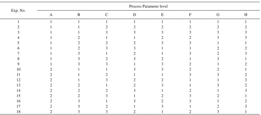
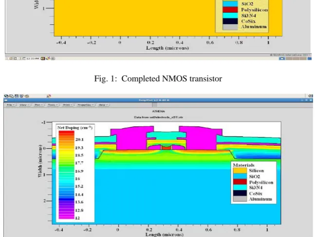
Figure 1 is a cross section of the complete simulated structure of a 32nm NMOS transistor and Figure 2 shows the doping profiles of the dopant in the transistor [10]. The results of threshold voltage (Vth) were analyzed and
processed with the Taguchi Method to get the optimal design. The optimized results from the Taguchi Method were simulated in order to verify the predicted optimal design.
Fig. 1: Completed NMOS transistor
Fig. 2: The doping profile of the NMOS transistor
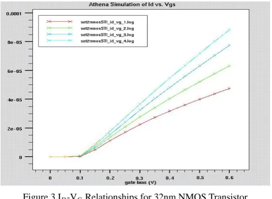
Electrical Characterization Simulation was performed by using the ATLAS module. ID -VG one of the main
parameters that were studied. The first part of the simulation is the drain current ID reaction to drain voltage VD
when gate voltage VG maintains its value. The process started by extracting the ID-VG relationship. For this VD
values were set between 0.05V, and 1.5V, and at each level, VG were swept from 0.0V to 0.8V with sub steps of
0.1V. Combining the graph for four VD values, the results are shown in Figure 3
Figure 3 ID-VG Relationships for 32nm NMOS Transistor
The threshold voltage (Vth) is the sum of the voltage drop Vs across the depletion layer and
the voltage drop Vox across the oxide when Vg = Vth The full equation for the threshold voltage requires the
addition of the flat band voltage to the oxide voltage drop and the depletion layer voltage drop. The threshold voltage (Vth) is expressed based on the Equation 4. [13]:
{
}
∗
+
+
=
+
+
=
1
/
2
0
2
1
ln
2
k
si
q
N
a
V
s
ox
C
ni
Na
KT*
Vfb
Vox
Vs
Vfb
Vth
ε
(4)Where
=
ni
Na
q
KT
Vs
2
*
ln
( the surface potential ) , (5)And
tox
Ksio
Cox
=
2
εo
, for silicon dioxide insulators (6)While tox is the thickness of the SiO2 oxide layer and Vfb the flat band voltage and ksi = 3.9.
Eighteen different experiments in the NMOS device were performed using the design parameter combinations in the specified orthogonal array table. Four specimens were simulated for each of the parameter combinations. The completed response for(Vth) data is shown in Table 4
Table 4 – Vth Values for NMOS Device
Exp. No
Threshold Voltage (Volts)
X1Y1 X1Y2 X2Y1 X2Y2 1 0.103118 0.103229 0.103111 0.103092 2 0.104293 0.103285 0.104367 0.105311 3 0.103147 0.103963 0.103910 0.103899 4 0.108381 0.112711 0.107947 0.107461 5 0.103116 0.103572 0.103964 0.103484 6 0.100235 0.100861 0.109768 0.100123 7 0.105675 0.104657 0.107658 0.106398 8 0.099418 0.107491 0.097856 0.092365 9 0.089261 0.093581 0.087469 0.083763 10 0.103762 0.104113 0.103138 0.102993 11 0.104265 0.104309 0.104274 0.104308 12 0.102011 0.102907 0.102148 0.103252 13 0.107992 0.108276 0.107486 0.107103 14 0.104103 0.104118 0.104195 0.104938 15 0.103914 0.103107 0.103025 0.102995
18 0.102924 0.102911 0.103256 0.102843
Eighteen experiments of the L18 array were performed, the next step was to determine which control factors had dominant effects on a device’s characteristics. Signal-to-noise (S/N) ratio was used to analyze the experimental data and to determine the optimal process parameter levels. There are three categories of performance characteristics in the analysis of the S/N ratio: the lower-the-better, the higher-the-better, and the nominal-the-better [7]. The S/N ratio for each level of process parameters is computed based on the S/N analysis. Regardless of the category of the performance characteristic, the larger S/N ratio corresponds to the better performance characteristic. Therefore, the optimal level of the process parameters is the level with the highest S/N ratio [14];[15].
In this research threshold voltage of the 32nm devices was considered to belong to the nominal-the-best quality. The nominal-the-best S/N Ratio was selected to get threshold voltage value closer (with reduced deviations) to a given target value (0.103V), which is also known as nominal value [15]. The S/N Ratio (Nominal-the-best) η can be expressed as Eq (1). By applying equations (1)-(3), the η for each device was calculated and given in Table 5 [7].
Table 5 – Mean, Variance and S/N Ratios for NMOS Device
Ex.
No.
A B C D E F G empty
Mean Variance S/N Ratio (Mean)
S/N Ratio (Nominal-the-Best)
1 1 1 1 1 1 1 1 1 0.10313 4.07E-09 -19.73 64.18
2 1 1 2 2 2 2 2 2 0.10432 6.84E-07 -19.63 42.02
3 1 1 3 3 3 3 3 3 0.10373 1.52E-07 -19.68 48.51
4 1 2 1 1 2 2 3 3 0.10912 5.85E-06 -19.24 33.08
5 1 2 2 2 3 3 1 1 0.10353 1.21E-07 -19.70 49.46
6 1 2 3 3 1 1 2 2 0.10275 2.20E-05 -19.76 26.81
7 1 3 1 2 1 3 2 3 0.10610 1.59E-06 -19.49 38.49
8 1 3 2 3 2 1 3 1 0.09928 3.91E-05 -20.06 24.02
9 1 3 3 1 3 2 1 2 0.08852 1.66E-05 -21.06 26.73
10 2 1 1 3 3 2 2 1 0.10350 2.77E-07 -19.70 45.87
11 2 1 2 1 1 3 3 2 0.10429 5.06E-10 -19.64 73.33
12 2 1 3 2 2 1 1 3 0.10258 3.56E-07 -19.78 44.70
13 2 2 1 2 3 1 3 2 0.10771 2.73E-07 -19.35 46.29
14 2 2 2 3 1 2 1 3 0.10434 1.62E-07 -19.63 48.28
15 2 2 3 1 2 3 2 1 0.10326 1.92E-07 -19.72 47.44
16 2 3 1 3 2 3 1 2 0.10488 1.13E-07 -19.59 49.88
17 2 3 2 1 3 1 2 3 0.10271 3.08E-06 -19.77 35.34
18 2 3 3 2 1 2 3 1 0.10298 3.43E-08 -19.74 54.91
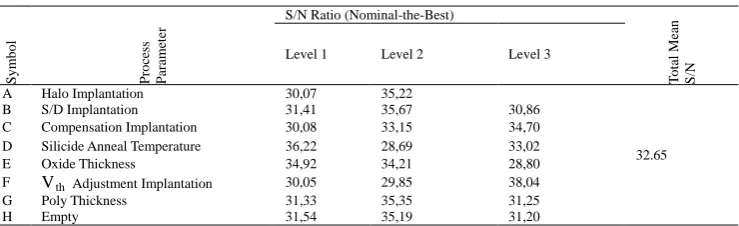
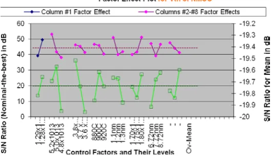
Referring to Table 5, S/N Ratios for the rows 1, 3, 5, 16 and 18 have 64.18 dB, 48.51 dB, 49.46 dB, 49.88 dB and 54.91 dB are given respectively. This result implies that process parameter combinations give the best insensitivity for the response characteristic. The effect of each process parameter on the S/N ratio at different levels can be distinguished because the experimental design is orthogonal. The S/N ratio for each level of the process parameters are summarized in Table 6. In addition, the total mean of the S/N ratio for the 18 experiments are also calculated and listed in Table 6.
Table 6 – S/N Ratio for the Threshold Voltage
S
ym
bo
l
P
roc
es
s
P
ar
am
et
er
S/N Ratio (Nominal-the-Best)
T
ota
l M
ea
n
S
/N
Level 1 Level 2 Level 3
A Halo Implantation 30,07 35,22
32.65
B S/D Implantation 31,41 35,67 30,86
C Compensation Implantation 30,08 33,15 34,70
D Silicide Anneal Temperature 36,22 28,69 33,02
E Oxide Thickness 34,92 34,21 28,80
F Vth Adjustment Implantation 30,05 29,85 38,04
G Poly Thickness 31,33 35,35 31,25
H Empty 31,54 35,19 31,20
Figure 4 shows the factor effect plots for the S/N Ratio (purple or magenta color) and the Mean (light green color) for the NMOS device. The dashed lines represent the values of the overall- mean of the S/N ratio and Mean respectively. Basically, the larger the S/N ratio the better the quality characteristic for the threshold voltage.
Figure 4 – S/N graph for threshold voltage in NMOS Device
A. Analysis of Variance (ANOVA)
The dominance of the process parameters with respect to the (Vth) was investigated to determine more
accurately the optimum combinations of the process parameters. The result of ANOVA for the NMOS device is presented in Tables 7. The percentage factor of the effect on S/N Ratio indicates the dominance of (process parameter) a factor to reduce variation. A factor with a high percent contribution will have a greater influence on the stability of (Vth) with respect to the noise parameters.
Table 7 – Result of ANOVA for NMOS Device
The results clearly show that the S/D Implantation (26%) has the most dominant impact to the S/N Ratio of the threshold voltage in the NMOS device, whereas Halo Implantation and Poly Thickness were the second ranking factors 18% and 15% respectively. These are the dominant factors. The percentage effects of oxide thickness and Vth Adjustment Implantation on the S/N ratio are lower, being 3% and 4.9% respectively. These are called
significant factors. The percentage effects of compensation implantation and silicide anneal temperature on the S/N ratio are also much lower, being 5% and 3% respectively. The best settings of dominant and significant factors could be found from the factor effect plots and the Analysis of Mean (ANOM) and these are A2B1E3F3G3 (Halo Implantation with value of 1.28x10¹³ atom/cm3, S/D Implantation with value of 5.2x10¹³ atom/cm3, Oxide Thickness with value of 1.3 nm, Vth Adjustment Implantation with value of 1.80 x 10¹¹
atom/cm3 and Poly Thickness with value of 8.72 nm). Because factors C (compensation implantation) and D (silicide anneal temperature) were found to have an insignificant or negligible effect on the nominal-the-best SNR, both of them can be pooled and they can be set at any level. Furthermore, one of the factors, C
S
ym
bo
l
P
roc
es
s
P
ar
am
et
er
De
gr
ee
of
F
re
ed
o
m
S
u
m o
f
S
q
ua
re
M
ea
n sq
ua
re
F
ac
to
r E
ff
ec
t
o
n
S
/N
R
at
io
(%) Fac
to
r E
ff
ec
t
on M
ea
n (
%
)
A Halo Implantation 1 478 478 18 5
B S/D Implantation 2 720 360 26 19
C Compensation Implantation 2 146 73 5 11
D Silicide Anneal Temperature 2 88 44 3 9
E Oxide Thickness 2 78 39 3 25
F Vth Adjustment
Implantation 2 135 67 4.9 8
G Poly Thickness 2 401 201 15 7
H Empty 2 421 210 15 5
“adjustment factor” as their effect on S/N ratio is negligible and their effect on Mean is large. The suitable levels for adjustment for C (compensation implantation) appear to be between C1 (3.8x10¹³ atom/cm3 ) and C2 (3.7x10¹³ atom/cm3 ) and for D (silicide anneal temperature) between D1 (880OC) and D2 (900OC). The full recommendation for this confirmation experiment was to perform 4 ‘fine-tuning’ simulations for factorial combinations of C1, C2 (3.8x10¹³ atom/cm3 , 3.7x10¹³ atom/cm3 ) and D1, D2 (880 OC , D2 900OC) then (C1D1 (3.7x10¹³ atom/cm3 , 880 OC), C1D2 (3.7x10¹³ atom/cm3 , 900 OC), C2D1 (3.8x10¹³ atom/cm3 , 880OC), C2D2 (3.8x10¹³ atom/cm3 , 900 OC)), keeping all other factors at their best settings A2 (Halo Implantation with value of 1.28x10¹³ atom/cm3 ), B1 (S/D Implantation with value of 5.2x10¹³ atom/cm3 ), (C1 or C2 , (compensation implantation with values of 3.8x10¹³ atom/cm3 or 3.7x10¹³ atom/cm3 )), (D1 or D2 (silicide anneal temperature with values of 880OC or 900 OC)), E3 (Oxide Thickness with value of 1.3 nm), F3 (Vth Adjustment Implantation
with value of 1.80 x 10¹¹ atom/cm3), G3 (Poly Thickness with value of 8.72 nm)). The aim of these 4 simulations was to get S/N ratio > 64.18, guaranteeing minimal (Vth) variability and at the same time to put the
value of (Vth) at the target value of 0.103V.
B. Confirmation of Optimum Run
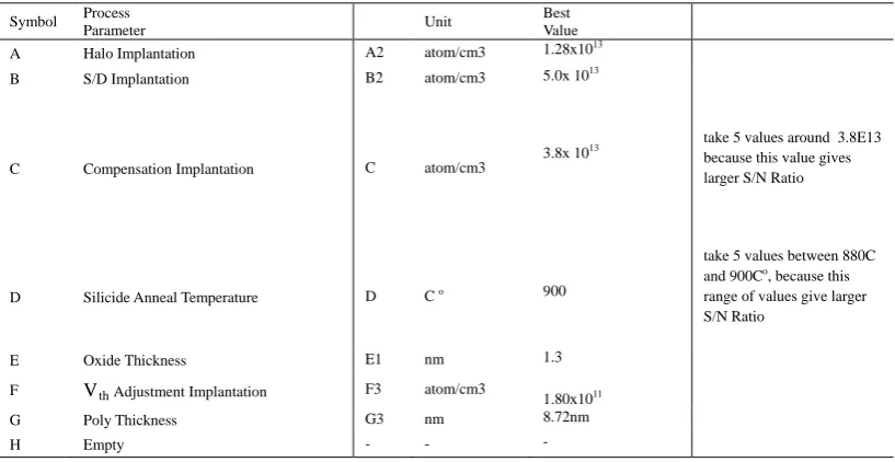
From the available information it can be clearly said that for the referred to design, either Compensation implantation (factor C) or silicide anneal temperature (factor D) could be defined as adjustment factors because these have a small effect on the S/N Ratio (variance) and a large effect on the mean. In the NMOS device, the value of compensation implantation or silicide anneal temperature can be adjusted. The fine tuned adjustments have to be done to get the threshold voltage closer to the nominal value or target value. The best setting of the process parameters for the device which has been suggested by the Taguchi method are compiled in Table 8.
Table 8 – Best Setting of the Process Parameters
Symbol Process
Parameter Unit
Best Value
A Halo Implantation A2 atom/cm3 1.28x10¹³
B S/D Implantation B2 atom/cm3 5.0x 10¹³
C Compensation Implantation C atom/cm3
3.8x 10¹³ take 5 values around 3.8E13
because this value gives larger S/N Ratio
D Silicide Anneal Temperature D C o 900
take 5 values between 880C and 900Co, because this
range of values give larger S/N Ratio
E Oxide Thickness E1 nm 1.3
F Vth Adjustment Implantation F3 atom/cm3 1.80x10¹¹
G Poly Thickness G3 nm 8.72nm
H Empty - - -
From the above parameters as shown in Table 8, the fine tuning simulations were performed to verify the accuracy of the Taguchi Method prediction.
The value of compensation implantation was varied within 3.7 x 10¹³ to 3.8 x 10¹³ and silicide annealing temperature varied within 880 Co to 900 Co, until the value of threshold voltage (Vth) closer to 0.103v. By doing
the value sweep, the optimum solution for fabricating a 32nm NMOS transistor is 3.73 x 10¹³ atom/cm3 and 885 Co. By adding noise factors to this simulation and run them :The following results are obtained which shown in Table 9.
Table 9 – Results of Further Runs of Confirmation
Experiment with Added Noises
Device X1Y1 X1Y2 X2Y1 X2Y2
NMOS 0.103134 0.1032041 0.1031862 0.1030652
From the above results further runs of confirmation experiments with added noises as shown in Table 9 were performed. For NMOS, the mean is 0.103147375 V with S/N ratio of 66 dB. The values are well within the target set by ITRS [16].
IV. Conclusion
The optimum solution in achieving the desired transistor was successfully predicted by using the Taguchi Method. A stable threshold voltage (Vth) is the main result of this simulation test. Leakage Current has also been kept to minimum. In this research, Compensation implant dose and silicide anneal temperature have been identified as the adjustment parameters for the threshold voltage, whereas Compensation implant dose alone has the strongest effect on reducing the leakage current for this device.
Acknowledgment
The authors would like to thank to the Institute of Microengineering and Nanoelectronics ( IMEN), Universiti Kebangsaan Malaysia (UKM), Centre for Micro and Nano Engineering (CeMNE) of College of Engineering Universiti Tenaga Nasional (UNITEN), Freescale (M) SDN,BHD. And Indian Institute of Technology (Bombay) (IITB) for their support throughout this project.
References
[1] Ashish Srivatsava, Tejasvi Kachru, Dennis Sylvester, “Low-Power-Design Space Exploration Considering Process Variation Using Robust Optimization,” IEEE Transactions on Computer-Aided Design of Integrated Circuits and Systems, Vol.26, No.1, 2007. 67-79
[2] S. Shedabale, H. Ramakrishnan, G. Russell, A. Yakovlev, and S. Chattopadhyay, "Statistical Modeling of the Variation in Advanced Process Technologies using a Multi-level Partitioned Response Surface Approach", IEEE , Circuits, Devices & Systems, IET, Vol.2, No.5, 2008 , 451-461
[3] Liang-Teck Pang, Borivoje Nikolic,(2006) “Impact of Layout on 90nmm Process Parameter Fluctuations”,IEEE Symposium on VLSI circuit Digest of Tecnical papers”, 2006,69-70
[4] H. Ramakrishnan, S. Shedabale, G. Russell, and A. Yakovlev, “Stacked Strained Silicon Transistors for Low-Power High-Performance Circuit Applications”, IEEE ECTC08, pp. 1793-1798, Florida, May. 2008. [5] R.H. Lochner, J.E. Matar, “Design for quality–An introduction to the best of Taguchi and Western methods of statistical experimental design”, New York, 1990
[6] P. Sharma, A. Verma, R.K. Sidhu, O.P. Pandey, “Process parameter selection for strontium ferrite sintered magnets using Taguchi L9 orthogonal design”, Journal of Materials Processing Technology 168 (2005) 147-151.
[7] Phadke, Madhav S., (1989). “Quality Engineering Using Robust Design”, Prentice Hall and (2008) Low Price Edition, Pearson Education, Inc.
[8] G.P. Syrcos, “Die casting process optimization using Taguchi methods”, Journal of Materials Processing Technology 135 (2003) 68-74.
[9] Leon, R. V., Shoemaker, A. C., and Kacker, R. N. (1987),” Performance Measures Independent of Adjustment: An Explanation and Extension of Taguchi's Signal-to-Noise Ratios (with discussions). Technometrics “,29, 253-285
[10] H.A. Elgomati, B.Y. Majlis, I. Ahmad,F. Salehuddin,2F.A. Hamid,A. Zaharim and P.R. Apte," Application of Taguchi Method in the Optimization of Process Variation for 32nm CMOS Technology",Australian Journal of Basic and Applied Sciences, 5(7): 346-355, 2011 , ISSN 1991- 8178.York, 2001.
[11] Roy R.K (2001) ,”Design of experiments using the taguchi approach”, John Willey&Sons. Inc., New. [12] Stephanie Fraley, Mike Oom, Ben Terrien, John Zalewski, “Design of experiments via taguchi methods: orthogonal arrays” Michigan Chemical Process Dynamics and Controls, 2006
https://controls.engin.umich.edu/wiki/index.php/Design_of_experiments_via_taguchi_methods:_orthogonal_arrays
[13] Y. Taur and T. H. Ning,“Fundamentals of Modern VLSI Devices”. New York: Cambridge Univ. Press, 1998, ch. 3, p. 130.
[14] Abdullah H., Jurait J., Lennie A., Nopiah Z.M., Ahmad I., (2009),”Simulation of Fabrication Process VDMOSFET Transistor Using Silvaco Software”, European Journal of Scientific Research, ISSN 1450-216X, Vol.29 No.4, pp. 461-470.
[15] The 17th International Conference on Flexible Automation and Intelligent Manufacturing, Vol.24, Issue 6, pp. 811-815.
[16] ITRS, 2008. Report; http://www.itrs.net