Flyback Converter Design and Simulation
Swati Kunkolkar1, V.N Shet2Student (ME power & Energy), Dept. of E&E, Goa Engineering College, Farmagudi, Goa, India1
Professor, Dept. of E&E, Goa Engineering College, Farmagudi, Goa, India2
ABSTRACT: This paper addresses a novel approach for designing and modelling of isolated interleaved flyback converter. A detailed design, simulation and PWM control strategy are conferred for flyback converter in DCM. To verify the design, the study of converter is practised in DCM operation for input AC voltage 200-250V at 50Hz and output DC voltage of 90V and 81W output rating using PSIM 6.0 software. A little ripple appears in output of the converter.
KEYWORDS: Flyback, Converter, THD (Total Harmonic Distortion), PF(Power Factor).
I. INTRODUCTION
Fly-back converter is the most commonly used SMPS circuit for low output power applications where the output voltage needs to be isolated from the input main supply. The output power of fly-back type SMPS circuits may vary from few watts to less than 100 watts. The overall circuit topology of this converter is considerably simpler than other SMPS circuits. Input to the circuit is generally unregulated dc voltage obtained by rectifying the utility ac voltage followed by a simple capacitor filter. The circuit can offer single or multiple isolated output voltages and can operate over wide range of input voltage variation. In respect of energy-efficiency, fly-back power supplies are inferior to many other SMPS circuits but it’s simple topology and low cost makes it popular in low output power range.
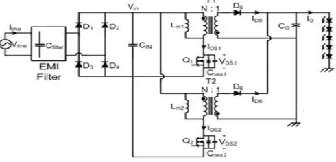
Figure 1 Interleaved Flyback converter.
II. LITRATURE SURVEY
Figure 2Flyback converter.
Primary and secondary windings of the transformer are wound to have goodcoupling so that they are linked by nearly same magnetic flux. The primary andsecondary windings of the fly-back transformer d’nt carry current simultaneouslyand in this sense flyback transformer works differently from a normal transformer.In a normal transformer, under load, primary and secondary windings conductsimultaneously such that the ampere turns of primary winding is nearly balancedby the opposing ampere-turns of the secondary winding (the small difference inampere-turns is required to establish flux in the non-ideal core). Since primaryand secondary windings of the y-back transformer donot conduct simultaneouslythey are more like two magnetically coupled inductors and it may be more appro-priate to call the flyback transformer as inductor-transformer. Accordingly the magnetic circuit design of a y-back transformer is done like that for an inductor.The output section of the flyback transformer, which consists of voltage rectification and filltering, is considerably simpler than in most other switched modepower supply circuits. As can be seen from the circuit Figure2, the secondary winding voltage is rectified and filtered using just a diode and a capacitor. Voltage across this filter capacitor is the SMPS output voltage.
III. PROPOSED SYSTEM
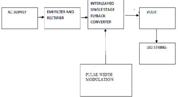
The single phase AC supply is fed to the EMI filter. EMI filter filters out the noises. The output of EMI filter is fed to the rectifier. Rectifier converts it to DC. The rectifier output is then fed to the interleaved flyback converter. The flyback converter is controlled by pulse width modulation. The regulated dc output is then fed to the LED string.
Error! Reference source not found.
shows the block diagramIn proposed method discontinuous mode of operation is adopted. This means there will be time delay between turn ON and turning OFF of the switching devices as a result the stress on switching devices will be less and hence efficiency will be more. The sinusoidal pulse width modulation technique is used to control the MOSFET in the flyback converter. In sinusoidal pulse width modulation, triangular wave is the carrier signal and the sine wave is the reference signal. The gating pulses are generated by comparing the reference signal with the carrier wave. This method reduces the power loss in switching device. Figure 1 Interleaved Flyback converter.shows the PWM signals that are fed to the MOSFET switches Q1 and Q2.
Advantages of interleaved flyback converter:
• Reduced transformer and semiconductor peak currents • Reduced transformer and semiconductor RMS currents • Reduced input and output capacitor RMS currents • Reduction of EMI energy due to lower peak currents • Distribution of heat generating elements
Disadvantages of interleaved flyback converter:
• Increased component count
• Possible increase in component area
• Control complexity of interleaved drive signals for Dmax greater than 50%
IV. DESIGN
Following assumptions are made for designing an interleaved flyback converter (
Error! Reference source not
found.
).Assumptions:
1. Transformer leakage inductances are negligible.
2. EMI filter is larger than input capacitance.
3. The magnetizing inductances Lm1 and Lm2 are identical.
4. There is 180deg phase shift between the two switches.
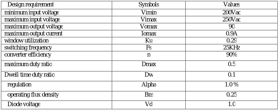
Table 1 Design requirements
Design requirement Symbols Values
minimum input voltage Vimin 200Vac
maximum input voltage Vimax 250Vac
maximum output voltage Vomax 90
maximum output current Iomax 0.9A
window utilization Ku 0.29
switching frequency Fs 25KHz
converter efficiency n 90%
maximum duty ratio Dmax 0.5
Dwell time duty ratio Dw 0.1
regulation Alpha 1.0 %
operating flux density Bm 0.25
1. calculate total period=T
=1= 1
25000 = 40
2. maximum on time= Ton
= ∗ = 40 ∗0.5 = 20
3. Rectifier output:
When Vinac=200V
= 2∗Vac − ∗1−
∗ = 268.84
When Vinac=250V
=√2∗ =√2∗250 = 353.55
4. maximum output power=Pomax
= ∗( + ) = 0.9∗(90 + 1) = 81
= 100
5. maximum input current, Iinmax
=
∗ =
100
268.84∗0.9= 0.41
6. calculate the primary peak current=Ippk
= 2∗ ∗
∗ ∗ = 1.65
7. calculate primary RMS current Iprms
= Ippk∗ Ton
3∗T= 0.67
8. maximum input power Pinmax
= ==100
0.9 = 111
9. equivalent input resistance Rineq
= ==268.84
10. primary magnetizing inductance L
= ∗ ∗
2 = 3.30
11. Energy handling capability in watts-sec, E
= ∗
2 =
3.30 ∗1.65
2 = 0.0045 −
12. Electrical conditions, Ke
= 0.000091
13. Core geometry, Kg
= 0.29
14. use core EE-625 (in U.S Standard)/ PC40EE47/39-Z
15. Calculate current density J
= 2∗ ∗10
∗ ∗ =
2∗0.0045∗10
0.25∗4.616∗0.29= 268.93 /
16. primary wire area, Apwb
= = 0.67
268.93= 0.00249
#23 AWG wire is required which has, Bare wire area=0.0025880cm2 If I use minimum #30 AWG wire with bare wire area= 0.0005097cm2
17. Number of primary strands, Snp
= =0.0025880
0.0005067= 5
18. Number of primary turns Np. Half of available window is primary Wap/2'; using no. of strands, Snp and BWA #23
Wa=1.930
=
2 =
1.930
= ∗
3∗ = 36
19. Required Gap lg
= 0.4∗ ∗ ∗ ∗10 −
Ω = 0.008
20. firing flux factor, F
= 1 +
√ ∗log
2∗
= 1.03
21. New number of turns, Nnp
= ( ∗ )
0.4∗ ∗ ∗ ∗10 = 29
22. Peak flux density, Bpk
=0.4∗ ∗ ∗ ∗ ∗10
+ Ω
= 0.53[ ]
23. New µΩ/cm
μ Ω =μ
Ω
=3420
5 = 684
24. primary winding resistance, Rp
= ∗ ∗ Ω ∗10 = 9.4∗29∗684∗10 = 0.18 Ω
25. primary copper loss, Pp
= ∗ = 0.67 ∗0.18 = 0.08
26. secondary turns, Ns
= ∗( + )∗(1− − )
27. Secondary peak currents, Is1pk
= 2∗
1− − = 4.5
28. Secondary RMS current, Isrms
= ∗ 1− −
3 = 1.64
29. Secondary wire area, Aswb
= = 1.64
268.93= 0.0060
30. number of secondary strands, Sns
= = 0.0060
0.0008046= 8
31. Secondary S, Ωpcm
Ω = Ω =2142
8 = 267.75
32. Winding resistance, Rs
= ∗ 1∗ 1 Ω ∗0.000001 = 0.020Ω
33. secondary copper loss, Ps
= ∗ = 1.64 ∗0.020 = 0.054
34. Total no. of turns
[ ] = ∗ = 29∗5 = 145
[ ] = 1∗ 1 = 8∗8 = 64
35. Total copper loss, Pcu
= + = 0.08 + 0.054 = 0.134
36. Calculate, Cin
= 2 ∗ = 2 ∗111 = 222μ
Use Cin=230µF
37. Calculate, Co Ncp=20;
= 0.05∗ = 0.05∗90 = 4.5
= ∗
∗ =
1∗20
25 ∗4.5= 177.77μ
Use Co=180µF or 189µF
38. Secondary and primary inductance.
=( + )∗(1− )
∗
= 5%∗
=(90 + 0.1)∗(1−0.5)
0.0045∗25 = 40
= ∗ = 16 ∗ 145
64 = 0.2
V. SIMULATION RESULTS
PSIM is a simulation software specially designed for fast simulation andfriendly user interface. PSIM provides powerful simulation environment toaddress my simulation needs. It also provides an intuitive and easy-to-use graphic user interface. for schematic editing. In addition, extensive onlinehelp is available for each component.
Figure 4(a1) shows PSIM model of single phase rectifier. To the rectifier wegive 200Vac signal to get rectified output DC voltage. We get average outputvoltage of 127.32Vdc. This is fed to the DC-DC interleavedflyback converter shown in figure 4(a2).
(a2)
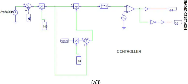
The controller circuit is shown in figure4(a3) which generate G1 and G2 PWMpulses with 180 deg phase shift. These PWM pulses as shown in figure4(a3)are fed to the MOSFET switches in figure4(a2).
(a3)
Figure 3 Single phase rectifier(a1),interleaved flyback converter (a2), controller (a3) PSIM model
Table 2 Simulation parameters.
Parameters Values
Vin 200-250Vac
Vo 90Vdc
Io 0.9A
Cin 230µF
Co 189 µF
Core PC40EE47/39-Z
Air gap 0.008cm
Nnp 29
No. of primary strands 5
No. of secondary strands 8
Magnetisin inductance Lm1=Lm2 3.3mH
Output resistance 100Ω
THD 1.66%
PF 0.46
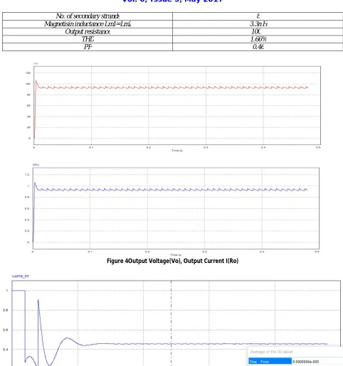
Figure 4Output Voltage(Vo), Output Current I(Ro)
Figure 6 THD graph
VI. CONCLUSION
A simple modeling method is presented. This is based on the equivalent circuit of converter in ON and OFF time period. The developed interleaved flyback converter circuit is simulated in PSIM software. PWM control strategy is applied. The proposed converter provided a regulated output with very low ripple content. In closed loop it gave 1.5% THD and 0.46 PF.
REFERENCES
[1] G. S. Sandhya. K, "An Interleaved Single-Stage Fly Back AC-DC converter for outdoor LED lighting," International Journal of Engineering Research & Technology, vol. 3, no. 3, pp. 1679-1683, March 2014.
[2] S.-W. L. a. H.-L. Do, "A Single-Switch AC-DC LED Driver Based on a Boost-Flyback PFC Converter with Lossless Snubber," IEEE transaction on power electronics, vol. 32, no. 2, pp. 1375-1384, 2017.
[3] A. A. Saliva, "Design Guide for Off-line Fixed Frequeny DCM Flyback Converter," january 2013.
[4] G.-B. K. G.-W. M. SangCheol Moon, "An Interleaved Single-Stage Flyback AC-DC Converter with Wide Output Power Range for Outdoor LED Lighting System," in Applied Power Electronics conference and exposition,2012 Twenty-seventh Annual IEEE, 2012.
[5] www.fairchildsemi.com
[6] C.W.T. McLyman, Tarnsformer and inductor Design Handbook.
[7] Brian Shaffer, Interleaving Contributes Unique Benefits to Forward Converters.
[8]