Resonator for Suppression of Higher Order Harmonics
Rakesh Kumar* and Shiva Nand Singh
Abstract—In this research paper, a Ridge Substrate Integrated Waveguide (RSIW) multiple band bandpass filter embedded with an octagonal shape Complementary Split Ring Resonator (CSRRs) is proposed. The electrically coupled octagonal shape CSRR is placed interdigitally in RSIW using transverse coupling technique to improve multiple passband bandwidths. The filter exhibits a highly selective multiple electric or magnetic or bianisotropic mode for different frequencies. The analysis for spurious band suppression has been done by direct method. The prototype configuration of quarter-wavelength octagonal CSRR resonators introduces band suppression at all odd harmonics. The proposed structure of filter with dimension 1.36λg×0.52λg excluding feed port is fabricated. Full wave structure
simulated results are compared with measurement ones. The measured passband frequencies and their calculated respective central frequency (f0), fractional bandwidth (FBW) are in close agreement with
the simulated result. The spurious higher order harmonics are observed as suppressed. The filter can be utilized to suppress interference from LAN, WLAN, GSM, WiMAX and variable stopband for ISM interference.
1. INTRODUCTION
Filters find wide application to maintain quality in communication systems. Metamaterial structures as used in filters have attracted considerable attention due to size shrinking and its unique properties [1]. The latest trend in wireless communication system needs miniaturized filters in association with integrated multifunctional and multiband accomplishment for suppressing interference. It has been demonstrated that ring resonator based filters have attractive behaviour [2–4], but they have certain drawbacks such as large dimension and existence of higher order mode. Microstrip lines are compact and less expensive but resulting in non-immunity to the losses and parasitic crosstalk between lines. less expensive but offer non-immunity to the losses as well as parasitic crosstalk between lines. In order to reduce filter size and enhance the performance, several modified waveguide configurations have been developed, such as substrate integrated waveguide (SIW) [5–7], half mode substrate integrated waveguide (HMSIW) [8, 9], substrate integrated slab waveguide [10–12], and ridge substrate integrated waveguide (RSIW) [13, 14] in SIW configuration. SIW supersedesf conventional rectangular waveguide by its reduced width due to substrate filling. In comparison to the conventional waveguide, it not only gives rise to limited bandwidth and high losses in terms of substrate dielectric loss but also contributes to additional metallization losses due to its reduced guided height. Hence, a ridge was introduced to SIW structure in order to enhance operating bandwidth [15–17].
A novel RSIW waveguide was introduced by Bozzi et al. [18] in which top and bottom metal layers are filled with dielectric substrate. To replicate the side wall, two rows of plated through hole via a
Received 4 August 2018, Accepted 6 December 2018, Scheduled 25 December 2018
* Corresponding author: Rakesh Kumar ([email protected]).
full height structure has been incorporated. In addition, a pair of partial-height via array holes in the center of the SIW and common fully plated-through vias as side walls have been used.
Recently, filters using SIW and RSIW structures loaded with cavity configuration [18], double circular ring [7], triangular ridge [19], slot array antenna [20] and several miniaturized filters structures [12, 16, 21] have been reported by several authors. The conventional spurious band suppression is mainly designed for the application of single-band rejection [22] of narrow bandwidth. Further design of microstrip bandpass filters with multi-order spurious-mode suppression has been reported by authors in [23–25]. Subsequently, a non-radiative interdigital finger structure RSIW [21, 26] targeting the design of compact SIW filter structure is designed by cascading odd multiple of quarter wavelength uniform transmission elements in line configuration. It has been observed in the above reported filters that a significant low fractional bandwidth with limited number of passbands and high insertion loss have been experienced in microstrip line and coplanar waveguide.
In this research work, octagonal shapes of CSRRs are etched on the ridge surface of SIW, and interdigital capacitance is formed along the direction of propagation. The middle metal plane is connected through metallic vias. The circuit elements and the resonance frequency of CSRRs are adjusted by its geometrical dimension. In this RSIW parallel capacitance and inductance are placed in series with the transmission line. These elements can be used to enhance the spurious suppression performance of the proposed bandpass filter. The proposed CSRRs embedded RSIW filter can preserve the energy flow and avoid the energy leakage. These resonators establish higher-order mode transmission due to the transversal coupling. Also, by using direct method the effective permittivity and permeability in higher order harmonics are extracted. The filter has odd integral multiple of different centre frequencies, and some of them have similar or the same resonating frequency to realize multiple band suppression also including source-load coupling. This composite structure inherits the merits of planar transmission lines such as miniaturized size, low cost and easy integration with other planar circuits.
2. DESIGN CONSIDERATION
2.1. Substrate Integrated Waveguide
The design of SIWT Em0n(wheremis the odd number, andnis a positive integer) modes can be excited.
The fundamental modeT E101 is analyzed for the generation of transmission zero to suppress the higher
order spurious response. In the SIW structure of Figure 1(a) desired passband to be generated and to improve spurious band suppression performance is constructed into dielectric substrate with = 2.5. The total height h = h1 +h2 = 3.2 mm, the metalized via diameter d2 = 0.35 mm, pitch
(centre-to-centre) spacingds2 = 0.65 mm, and a= 6 is the spacing between the two arrays. The cutoff frequency
of the dominant mode in the SIW [5] is given as
fm0n=
1 2π√μ
mπ aSIW 2 + nπ lSIW 2
, [Hz] (1)
where,
aSIW = a−1.08
d22 ds2
+ 0.1d
2 2
a (2)
lSIW = a−1.08
d22 ds2
+ 0.1d
2 2
l (3)
The synthesized waveguide becomes free from leakage loss by selecting a proper via diameter (d2) and pitch (ds2) dimension. The resonance frequency of its dominant mode is f101 = 15.56 GHz,
f102 = 17.67 GHz and f103 = 23.03 GHz, respectively, as shown in Figure 1(b) and results in wider
monomode bandwidth than the rectangular waveguide. For further improvement, the bandwidth of SIW is indeed widened with an RSIW.
2.2. Ridge SIW (RSIW)
(a) (b)
Figure 1. (a) Layout of the SIW resonator (all dimensions are in mm: a = 14 mm, ds2 = 0.65 mm,
d2 = 0.35 mm, h= 3.2 mm) (grey region is metal, green region is substrate). (b) Mode plot.
(a) (b)
Figure 2. (a) Layout and design parameters of a single RSIW (all dimensions are in mm: a= 14 mm, b = 9 mm, d1 = 0.3 mm, d2 = 0.35 mm, dif = 0.5 mm, h1 = h2 = 1.6 mm, ds2 = 0.65 mm). (b)
Equivalent circuit of ridge waveguide (Lumped element value: C= 0.94 pf, L= 8.04 pH).
rectangular waveguide mono-modal cutoff f1 for dominant mode (T E10) for that height to width ratio
should be less than half. A ridge waveguide of a uniform multilayer substrate in which two rows of via array form side-walls, and two row of posts with central interdigital and bottom metal layer form central ridge, shown in Figure 2(a).
The resonance frequency for the dominant mode (T E10) in ridge waveguide [14] is given as
fc=
1
2π√LC (4)
where,
L= μ(a−b)
4 (h1+h2)
whereh1 andh2 are the thickness of top and bottom substrate layers respectively, and the capacitance
Cis the summation of electrostatic capacitance (Cg) and discontinuity capacitance (Cd) per unit length.
C=Cg+ 2Cd (5)
where,
Cg=
b h2
and
Cd=
π
x2+ 1 x cosh
−1 1 +x2
1−x2 −ln
4x 1−x2
where x = 1− h1
h1+h2. Figure 2(b) depicts the equivalent circuit of single RSIW at cutoff frequency.
Here the outer dimensions of the waveguides aand b remain unchanged. Further, through a suitable selection of the geometry of ridge the bandwidth of this waveguide can be controlled.
waveguide side walls which result in non-propagation of wave longitudinally. The cutoff frequency fc
of the dominant mode is calculated using MATLAB software from its equivalent circuit, and the cutoff frequency obtained is 22.53 GHz. By adjusting the width (a) and height (h1+h2) which is higher than
the first two modes and lower than the second higher-order mode in multilayer RSIW can change the cutoff frequency.
2.3. Characterization of CSRR Unit Cell
The proposed chiral octagon-shaped complementary split ring resonators have been used in waveguide. These resonators are placed at center of the transverse plane to excite the dominant mode of the waveguide T E10. The classical synthesis method [27] and multiple tunning procedures [28] are used
to determine the line width and gap spacing between the two octagonal CSRRs to obtain required characteristics and resonance frequencyfres= 2l√C0
eff wherelis the perimeter of octagonal loop resonator andeff the effective dielectric permittivity. The dimensions of resonators are chosen much smaller than
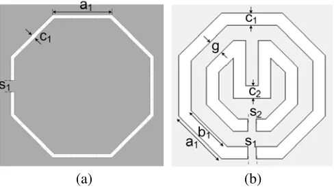
the wavelength of an incident electromagnetic wave, which results in bandstop nature at the resonances. The proposed double ring loaded CSRR as shown in Figure 3 and its dimensions are given below: the side of the outer ring a1 = 1.71 mm, slit width s1 = 0.45 mm, s2 = 0.22 mm, width of the ring
c1 =c2 = 0.25 mm, side of the inner ring b1 = 1.46 mm, and gap g = 0.48 mm between the ring. The
two resonators will offer independent resonant frequency at 4.25 GHz, by variation of electrical length of the resonator resulting in change of resonant frequency.
(a) (b)
Figure 3. (a) Basic unit CSRR (left). (b) Double-ring stub-loaded CSRR (right) (grey region is metal, white region is substrate).
3. STRUCTURE OF RSIW WITH OCTAGONAL CSRR AND ITS ANALYSIS
Figure 4 shows three-dimensional view of the structure composed of three metal layers, which are separated from one another by two similar thin dielectric substrate Arlon AD250A (tm) with dielectric constant r = 2.5; tanδ = 0.0015 and total substrate thickness h(h1 +h2) = 3.2 mm in which the
ridge substrate thickness h1 = 1.6 mm and 1st layer of substrate thickness h2 = 1.6 mm as shown in
Figure 2. The top and bottom metal layers consisting of a metal surface with common metallic via array. In addition to this bottom PCB with copper layered on both sides having one more metallic via array, consider a section of RSIW with octagonal CSRRs configured in odd number in the middle of a rectangular metallic plate and circular metallic post. A side view of the RSIW is presented in Figure 2(a). An adhesive film is used to stick the two substrates together with thickness 0.03 mm, dielectric constant r= 3, and loss tangent 0.0012.
Figure 4. 3D layout of the proposed inset feed coplanar waveguide to RSIW transition structure. The structure has been fabricated on an Arlon AD250A (tm) substrate with dielectric constant r = 2.5.
Actual device length (including access lines) is 68.2 mm.
(a)
(b)
(c)
(d)
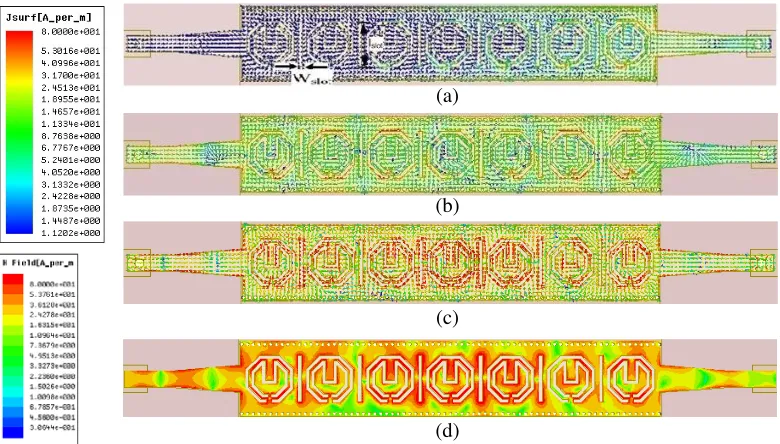
Figure 5. Simulated surface current distribution on interdigital layer of RSIW (whereWslot= 0.4 mm
andlslot= 4 mm), (a) at 4.67 GHz, (b) at 15.56 GHz, (c) at 20.7 GHz, (d) magnetic field distribution at
the resonance frequency of 20.7 GHz (5th harmonics of CSRRs).
offer two relative independent resonant frequencies which consist of two concentric octagonal individual rings. The outer ring is responsible for the smaller frequency band operation, while the coupling at the higher frequency band is achieved by the inner slot ring with a U-extension. The neighbouring resonators can be coupled through the transverse slot widthWslotas shown in Figure 5. The resonance
by the unloaded quality factor Q = 1976. The higher order harmonics (i.e., 3rd and 5th) of CSRRs are 12.75 GHz & 21.25 GHz under dominant mode of RSIW, respectively, while the cutoff frequencies of SIW and RSIW are 15.56 GHz and 22.53 GHz, respectively. It has been observed that SIW and RSIW cutoff frequencies are less than or equal to the 3rd and 5th order spurious frequency responses of CSRRs. By proper orientation and dimension of resonator, as well as waveguide, up to the 5th order of spurious harmonic can be suppressed. The construction scheme of octagonal CSRR offers an RSIW filter with improved higher order harmonic suppression [29] of a transversal filter using composite right/left-handed (CRLH) transmission line (TL). The electromagnetic energy gathers at center of the resonators for odd mode, and it is accumulated around the resonators for even mode. The resonance frequencies of the array of these chiral resonators provide good passband around the spurious band. As the distance between the resonators is multiple of λ4g, it has formed impedance transformer and perfect matching between cascaded resonators. The two concentric split rings which contain a CSRR loaded etched transmission line on a metallic surface are shown in Figure 4. The idea is derived by the application of principle of Babinet to the SRR [3, 19]. The principle states, in a case of complementary structure, roles are interchanged in terms of electrical as well as magnetic fields and currents [27]. The electric field mainly excites small electrical CSRR dimensions [28]. This symmetric CSRR is placed in the direction of propagation to perturbe the energy traveling along the central waveguide section. Figures 5(a)–(d) show the odd and even modes of typical distribution of current. Here, the splitting of signals into two paths consists of weighting of different amplitudes and delay in time. It is clearly indicated that the accumulation of electromagnetic energy around the center gap takes place for the odd mode, and it is also found gathered around the outer metallic edges for the even mode. In the above mentioned odd mode, a faster propagation than even mode takes place, i.e.,βo< βe. Therefore,
if a coupled section with identical even and odd mode electrical lengths, then traveling path for odd mode should be extended to merge the multipath signals at the output where interference is generated. Spurious band suppression characteristics of proposed filter can be computed by using direct method of electromagnetic parameter retrieval real and imaginary parts of effective electromagnetic parameters (eff and μeff) given by Smith et al. [30] for homogeneous medium, thereby applying the formula as
given by Smith et al. [30]:
z =
(1 +S11)2−S212
(1−S11)2−S212
(6)
n = 1 kdcos
−1
1 2S21
(1−S212 −S112 )
(7)
where ‘z’ is the impedance, ‘n’ the refacive index, ‘d’ the thickness of the substrate, ‘k’ the wave number, and ‘S11’ & ‘S21’ are the scattering parameters. The effective values of permittivity and permeability
are evaluated through the relationship of reflective index ‘n’ and impedance ‘z’ as given by eff =
n
z and μeff =nz. (8)
These formulae essentially require to compute eff and μeff from simulated scattering parameter,
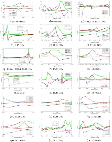
which are plotted in Figure 6. ‘S21’ is zero in the case of metamaterial based filter because of having
complete metal plate as ground. The real and imaginary parts of effective electromagnetic parameters (eff and μeff) are plotted in Figure 6. At peak absorption frequencies eff and μeff change rapidly
which show the electric and magnetic resonances.
(d) 9.45 GHz (e) 11.68 GHz (f) 12.88 GHz
(g) 13.22, 13.83 & 14.14 GHz (h) 15.38 GHz (i) 15.84 GHz
(j) 16.02 GHz (k) 18.48 GHz (l) 18.87 GHz
(m) 19.28 GHz (n) 19.41 GHz (o) 19.82 GHz
(p) 20.11 GHz (q) 20.7 GHz) (r) 21.58 GHz
Figure 6. Retrival of electromagnetic parameter eff and μeff from the simulated S-parameters at
4. EXPERIMENTAL RESULTS AND DISCUSSIONS
The individual building blocks of the designed compact, transversal coupled CSRR planner RSIW filter are mentioned in their respective sections of this paper. In order to experimentally verify the filter characteristics for suppressing spurious responses, a set of these resonators (which is electric, magnetic or both coupling) was etched on a metallized microwave substrate. Its scattering parameters are outlined in three different ranges i.e., (a) — (3.5 GHz–8 GHz), (b) — (8 GHz–15 GHz), (c) — (15 GHz–23 GHz) in Figure 7 and Figure 9, respectively. The response curves for fractional bandwidth, insertion loss, in-band return loss and transmission zero positions are analyzed. The structure simulation is carried out using Ansofts High Frequency Structure Simulation (HFSS), and theoretical analysis is done through MATLAB.
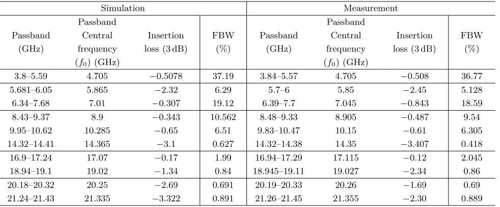
The filter exhibits a highly selective spurious band suppression performance with ten distinctive passbands centering at 4.705, 5.85, 7.045, 8.905, 10.15, 14.35, 17.115, 19.027, 20.26 and 21.335 GHz with 3-dB fractional bandwidths of 36.77%, 5.128%, 18.59%, 9.54%, 6.305%, 0.418%, 2.045%, 0.86%, 0.69%, and 0.889%, respectively. The minimum insertion losses at the ten passbands are−0.508,−2.45,
−0.843, −0.487,−0.61,−3.407, −0.12,−2.34,−1.69, and −2.3 dB, respectively. The transmission zero position is shown in Figure 9 at 5.65 GHz, 6.09 GHz, 7.88 GHz, 8.28 GHz, 8.42 GHz, 9.45 GHz, 11.68 GHz, 12.88 GHz, 13.22 GHz, 13.83 GHz, 14.14 GHz, 15.38 GHz, 15.84 GHz, 16.02 GHz, 18.48 GHz, 18.87 GHz, 19.28 GHz, 19.41 GHz, 19.82 GHz, 20.11 GHz, 20.7 GHz & 21.58 GHz.
(a)
(b)
(c)
(a)
(c)
Figure 8. Photographical image of the fabricated filter. (a) Prototype design frame work of proposed filter. (b) Top and (c) bottom views.
(a)
(b)
(c)
These resonances lead to absorption of propagating power from port 1 to port 2, and hence spurious higher order harmonics get suppressed. The proposed RSIW structure is designed to enhance rejection bandwidth as well as the coupling between the resonators which results in reduction in the dimension of spurious band eliminator filter [31, 32].
Photographs of the fabricated filter are shown in Figure 8 with inset feed SMA connectors. Photolithography process on a printed circuit board substrate material Arlon AD250A (tm) with dielectric constantr = 2.5 and tanδ= 0.0015, in which the ridge substrate thicknessh1= 1.6 mm, and
Table 1. Summary of in-band bandpass filter performance.
Simulation Measurement Passband (GHz) Passband Central frequency (f0) (GHz)
Insertion loss (3 dB)
FBW (%) Passband (GHz) Passband Central frequency (f0) (GHz)
Insertion loss (3 dB)
FBW (%)
3.8–5.59 4.705 −0.5078 37.19 3.84–5.57 4.705 −0.508 36.77
5.681–6.05 5.865 −2.32 6.29 5.7–6 5.85 −2.45 5.128
6.34–7.68 7.01 −0.307 19.12 6.39–7.7 7.045 −0.843 18.59
8.43–9.37 8.9 −0.343 10.562 8.48–9.33 8.905 −0.487 9.54
9.95–10.62 10.285 −0.65 6.51 9.83–10.47 10.15 −0.61 6.305
14.32–14.41 14.365 −3.1 0.627 14.32–14.38 14.35 −3.407 0.418
16.9–17.24 17.07 −0.17 1.99 16.94–17.29 17.115 −0.12 2.045
18.94–19.1 19.02 −1.34 0.84 18.945–19.11 19.027 −2.34 0.86
20.18–20.32 20.25 −2.69 0.691 20.19–20.33 20.26 −1.69 0.69
21.24–21.43 21.335 −3.322 0.891 21.26–21.45 21.355 −2.30 0.889
Table 2. Comparison between proposed multiband bandpass filter with already reported filters.
Reference Passband number Passband frequencies (GHz) Insertion loss (dB) FBW (%) In-Band Return Loss (dB)
Size (λ2
g)
[33] 2 0.895/2.42 0.9/1.65 12/4.1 Better than−13 0.011
[34] 3 1.57/2.45/3.65 −2.5/−1.9/−2.9 3.8/6.8/5 Better than−20 0.046
[35] 4 1.525/2.75
3.29/4.47
−4.42/−2.63
−3.03/−5.11
3.15/3.34
3.1/2.33 Better than−13 0.02
[36] 4 1.79/2.29
3.11/3.4
−1.34/−2.98
−3.12/−1.58
4.58/1.00 0.8/4.21
−20.49/−15.8
−14.6/−14.3 0.0729
[37] 5 0.6/0.9/1.2
1.5/1.8
−2.8/−2.9/−2.9
−2.6/−2.3
5.8/5.2/5.8
8.2/8.0 Better than−13 0.23
[38] 6 0.8/1.1/1.4
1.7/2/2.3
−2.13/−2.3/−2.26
−2.18/−2.08/−2.76
2.6/2.3/2
1.8/1.6/1.3 Better than−11 0.048
[39] 6 0.92/1.34/1.77
2.19/2.61/3.02
−0.76/−1.14/−2.13
−2.05/−2.48/−2.22
9.3/8.5/3.3 4.4/2.8/3 11.1/15.2/11.5 13.3//15.3/15.7 0.22 Proposed Work 10 4.705/5.85/7.045 8.905/10.15/14.35 17.115/19.027 20.26/21.335
−0.508/−2.45/−0.843
−0.487/−0.61/−3.407
−0.12/−2.34
−1.69/−2.3
36.77/5.128/18.59 9.54/6.305/0.418
2.045/0.86 0.69/0.889
−9/−10.18/−15.75
−12.3/−18.5/−12.28
−17.12/−14.01
−13.53/−21.01
are depicted in Table 1, and Table 2 compares the proposed bandpass filter with previously reported literature. Good agreement between measured and simulated results thus validate the proposed design concept.
The fabricated filter overall dimension excluding feed port is only 36.2 mm×14 mm which amounts to 1.36λg ×0.52λg, where λg is the guided wavelength. The prototype configuration of
quarter-wavelength octagonal CSRR resonators as depicted in Figure 3 introduces stopband at all odd harmonics. As designed, the cascaded resonator has eliminated up to 5th harmonics of 4.25 GHz (21.25 GHz) and 3rd harmonics at 12.75 GHz shifted to 20.7 GHz and 11.68 GHz of CSRR, respectively. However, the proposed multiple passband bandpass structure could not maintain constant bandwidth as observed due to low-quality factor. This filter can be effectively used for the application of multimode modern communication system and to suppress interference from LAN, WLAN, GSM, WiMAX and variable stopband for ISM interference.
5. CONCLUSIONS
This paper presents the design and analysis of a novel RSIW bandpass filter having dimension 1.36λg×
0.52λg with octagonal CSRR. Compared with conventional resonator, the cascaded configuration of
dual-pole resonators of RSIW filter provides compactness and harmonica control, and the reduction in bandwidth of stopband is improved through proper positioning of transmission zero. The proposed filter has suppressed the 3rd and 5th harmonics of resonance frequency of CSRR to 11.68 GHz and 20.7 GHz, respectively. Full wave structure simulated results are compared with measured ones with close agreement. The proposed filter can be effectively used for the application of multimode modern communication system and used to suppress interference from LAN, WLAN, GSM, WIMAX and variable stopband for ISM interferences.
REFERENCES
1. Caloz, C. and T. Itoh, “The engineering approach,”Electromagnetic Metamaterials: Transmission Line Theory and Microwave Applications, 2006.
2. Hsieh, L.-H. and K. Chang, “Compact, low insertion-loss, sharp-rejection, and wide-band microstrip bandpass filters,”IEEE Transactions on Microwave Theory and Techniques, Vol. 51, No. 4, 1241– 1246, 2003.
3. Sun, S. and L. Zhu, “Wideband microstrip ring resonator bandpass filters under multiple resonances,”IEEE Transactions on Microwave Theory and Techniques, Vol. 55, No. 10, 2176–2182, 2007.
4. Zhang, C. A., Y. J. Cheng, and Y. Fan, “Quadri-folded substrate integrated waveguide cavity and its miniaturized bandpass filter applications,” Progress In Electromagnetics Research C, Vol. 23, 1–14, 2011.
5. Kumar, R. and S. N. Singh, “Compact Substrate Integrated Waveguide multiband band pass filter using octagonal complementary split ring resonators,”International Journal of Applied Engineering Research, Vol. 12, No. 20, 10 127–10 133, 2017.
7. Che, W., C. Li, K. Deng, and L. Yang, “A novel bandpass filter based on complementary split rings resonators and substrate integrated waveguide,” Microwave and Optical Technology Letters, Vol. 50, No. 3, 699–701, 2008.
8. Senior, D. E., X. Cheng, and Y. K. Yoon, “Dual-band filters using complementary split-ring resonator and capacitive loaded half-mode substrate-integrated-waveguide,” 2012 IEEE Antennas and Propagation Society International Symposium (APSURSI), 1–2, IEEE, 2012.
9. Ur Rehman, M. Z., Z. Baharudin, M. A. Zakariya, M. H. M. Khir, M. T. Jilani, and M. T. Khan, “RF MEMS based half mode bowtie shaped substrate integrated waveguide tunable bandpass filter,” Progress In Electromagnetics Research C, Vol. 60, 21–30, 2015.
10. Bozzi, M., D. Deslandes, P. Arcioni, L. Perregrini, K. Wu, and G. Conciauro, “Efficient analysis and experimental verification of substrate-integrated slab waveguides for wideband microwave applications,” International Journal of RF and Microwave Computer-Aided Engineering, Vol. 15, No. 3, 296–306, 2005.
11. Ramesh, S. and T. Rama Rao, “Dielectric loaded exponentially tapered slot antenna utilizing substrate integrated waveguide technology for millimeter wave applications,” Progress In Electromagnetics Research C, Vol. 42, 149–164, 2013.
12. Chen, L.-N., Y.-C. Jiao, Z. Zhang, and F.-S. Zhang, “Miniaturized substrate integrated waveguide dual-mode filters loaded by a series of cross-slot structures,”Progress In Electromagnetics Research C, Vol. 29, 29–39, 2012.
13. Hopfer, S., “The design of ridged waveguides,” IRE Transactions on Microwave Theory and Techniques, Vol. 3, No. 5, 20–29, 1955.
14. Kazemi, R. and A. E. Fathy, “Design of a wideband eight-way single ridge substrate integrated waveguide power divider,”IET Microwaves, Antennas&Propagation, Vol. 9, No. 7, 648–656, 2014. 15. Li, C., W. Che, P. Russer, and Y. Chow, “Propagation and band broadening effect of planar ridged substrate-integrated waveguide (RSIW),” International Conference on Microwave and Millimeter Wave Technology, 2008. ICMMT 2008, Vol. 2, 467–470, IEEE, 2008.
16. Cheng, Y. J., C. A. Zhang, and Y. Fan, “Miniaturized multilayer folded substrate integrated waveguide butler matrix,”Progress In Electromagnetics Research C, Vol. 21, 45–58, 2011.
17. Han, S., X.-L. Wang, and Y. Fan, “Analysis and design of multiple-band bandstop filters,”Progress In Electromagnetics Research, Vol. 70, 297–306, 2007.
18. Bozzi, M., S. A. Winkler, and K. Wu, “Novel compact and broadband interconnects based on ridge substrate integrated waveguide,”IEEE MTT-S International Microwave Symposium Digest, 2009. MTT’09, 121–124, IEEE, 2009.
19. Huang, L. and H. Cha, “Compact ridge substrate integrated waveguide filter with transmission zeros,” IEEE Microwave and Wireless Components Letters, Vol. 25, No. 12, 778–780, 2015. 20. Mallahzadeh, A. and S. Mohammad-Ali-Nezhad, “A low cross-polarization slotted ridged SIW
array antenna design with mutual coupling considerations,” IEEE Transactions on Antennas and Propagation, Vol. 63, No. 10, 4324–4333, 2015.
21. Bahrami, H., M. Hakkak, and A. Pirhadi, “Analysis and design of highly compact bandpass waveguide filter using complementary split ring resonators (CSRR),”Progress In Electromagnetics Research, Vol. 80, 107–122, 2008.
22. Gil, M., J. Bonache, and F. Martin, “Metamaterial filters: A review,”Metamaterials, Vol. 2, No. 4, 186–197, 2008.
23. Chen, C.-F., T.-Y. Huang, and R.-B. Wu, “Design of microstrip bandpass filters with multiorder spurious-mode suppression,” IEEE Transactions on Microwave Theory and Techniques, Vol. 53, No. 12, 3788–3793, 2005.
28. Winkler, S. A., W. Hong, M. Bozzi, and K. Wu, “Polarization rotating frequency selective surface based on substrate integrated waveguide technology,” IEEE Transactions on Antennas and Propagation, Vol. 58, No. 4, 1202–1213, 2010.
29. Ji, Y., X. S. Yao, and L. Maleki, “High-Q whispering gallery mode dielectric resonator bandpass filter with microstrip line coupling and photonic bandgap mode-suppression,”IEEE Microwave and Guided Wave Letters, Vol. 10, No. 8, 310–312, 2000.
30. Smith, D., D. Vier, T. Koschny, and C. Soukoulis, “Electromagnetic parameter retrieval from inhomogeneous metamaterials,” Physical Review E, Vol. 71, No. 3, 036617, 2005.
31. Rambabu, K., M.-W. Chia, K. M. Chan, and J. Bornemann, “Design of multiple-stopband filters for interference suppression in UWB applications,” IEEE Transactions on Microwave Theory and Techniques, Vol. 54, No. 8, 3333–3338, 2006.
32. Yang, T., P.-L. Chi, R. Xu, and W. Lin, “Folded substrate integrated waveguide based composite right/left-handed transmission line and its application to partialH-plane filters,”IEEE Transactions on Microwave Theory and Techniques, Vol. 61, No. 2, 789–799, 2013.
33. Xu, J., W. Wu, and G. Wei, “Compact multi-band bandpass filters with mixed electric and magnetic coupling using multiple-mode resonator,”IEEE Transactions on Microwave Theory and Techniques, Vol. 63, No. 12, 3909–3919, 2015.
34. Zhan, X., Z.-X. Tang, H. Liu, Y. Wu, and B. Zhang, “Compact multiband transversal bandpass filters with multiple transmission zeroes,”Progress In Electromagnetics Research, Vol. 34, 157–167, 2012.
35. Lin, S.-C., “Microstrip dual/quad-band filters with coupled lines and quasi-lumped impedance inverters based on parallel-path transmission,” IEEE Transactions on Microwave Theory and Techniques, Vol. 59, No. 8, 1937–1946, 2011.
36. Gorur, A. K. and C. Karpuz, “Design of compact multi-band microstrip bandpass filter having simultaneously excited passbands by using open-circuited stubs,” IEEE MTT-S Int. Microwave Symp. Dig., 1–3, 2013.
37. Chen, C., “Design of a compact microstrip quint-band filter based on the tri-mode stub-loaded stepped-impedance resonators,”IEEE Microwave and Wireless Components Letters, Vol. 22, No. 7, 357–359, July 2012.
38. Tu, W.-H. and K.-W. Hsu, “Design of sext-band bandpass filter and sextaplexer using semilumped resonators for system in a package,” IEEE Transactions on Components, Packaging and Manufacturing Technology, Vol. 5, No. 2, 265–273, 2015.