George Shaker1, 2, *, Safieddin Safavi-Naeini1, and Nagula Sangary1, 3
Abstract—In this paper, the modal theory of antennas is re-visited, believing that it brings invaluable information towards facilitating the design of multi-feed multi-band antennas. First, some subtle changes are proposed to enhance the applicability of the theory. Next, using some efficient computational techniques, the proposed formulations are shown to predict, to a very high accuracy, the input impedance of any antenna under study. This greatly simplifies the antenna problem and focuses design efforts on finding the appropriate complex resonance frequency to cover a required band. Finding the appropriate feed location is then a matter of extracting the corresponding impedance map for this antenna through simple field manipulations.
1. BACKGROUND
Modal analysis among the circuit and filter communities is widely spread. A close look at the design steps of many of the available modern filters reveals the utilization of modal techniques as a key design component [1]. Notably, modal analysis of antennas has long been known in the antenna community. Lo and Richards contributed significantly to the advancement of this theory in the late 1970s and early 1980s [2]. However, their approach was limited in its accuracy due to the utilization of some theoretical assumptions of the complex resonant frequencies of the antennas they studied. These assumptions imposed significant limitations on the antennas’ structures that could be analyzed, along with limitations on the achievableQvalues. To date, modal analysis in antenna design has not evolved at the same rate it did in circuit/filter applications.
There exists a plurality of work on antenna analysis using modal expansion techniques. The work of Harrington and Mautz is one example [3], and the work of Shen and MacPhie is another [4]. Remarkably, the analysis and design of printed antennas is widely documented in numerous research papers and assembled in several books (see for example [5–23]). In its simplest form, a planar printed antenna is modeled as a transmission line model with its radiating edges treated as slots. A more rigorous analysis came in 1977 by Professor Lo [2] who treated the planar printed antenna as a cavity. His work was amended by multiple refinements to the modal approach for antenna design [14, 15]. However, the research following his approach essentially diminished since the early 1990s with rare subsequent occurrences in publications. This is primarily due to the limited accuracy of the approach when dealing with practical antenna designs. The limited accuracy was mainly attributed to the approximate calculation of the complex resonant frequency. This means that if such a frequency were calculated to a higher accuracy, then the technique would result in much better results. This will be the main focus of this chapter.
Although the transmission-line model is easy to use, it suffers from numerous disadvantages [11]. For instance, it is only useful for patches of rectangular shape, the fringe factor must be empirically determined, it ignores field variations along the radiating edge, and it is not adaptable to inclusion of
Received 28 January 2015, Accepted 4 March 2015, Scheduled 13 March 2015 * Corresponding author: George Shaker ([email protected]).
the feed. These disadvantages are diminished in the modal expansion analysis technique, whereby the patch is viewed as a thin cavity with magnetic walls. In this technique, the field between the patch and the ground plane is expanded in terms of a series of cavity resonant modes or Eigen functions, along with its eigenvalues or resonant frequencies associated with each mode. The effect of radiation and other losses is represented in terms of either an artificially increased substrate loss tangent [11] or by the more elegant method of an impedance boundary condition at the walls [2–8]. In fact, the later method results in a much more accurate formulation for the input impedance and resonant frequency for rectangular, circular, and other simple geometrical patches, at only a modest increase in mathematical complexity. However, it remains quite limited when irregular geometries are considered.
Thus, given the prior art, there are two major approximations with the modal theory that need to be studied: the use of the impedance boundary condition, and the effect of radiation on the orthogonality condition and all of the associated formulations.
2. MODERN EIGEN MODE SOLVERS
It can be shown that one way to realize anRLC equivalent network for an antenna is to have accurate knowledge of the value of the complex modal resonance frequencyωmn. Using approximate impedance boundary conditions is limited in its application to antennas with simple configurations and high Q
values. Moreover, modern antenna designs typically feature structures with several slots, along with relatively low Q values. This severely limits the utilization of the concept of impedance boundary conditions for such a problem.
One possible alternate method, given the advancements in the computational powers and techniques, is to utilize a generalized EM Eigen solver. Several numerical Eigen solvers found their way recently into leading commercial EM software, targeting applications in acoustics, photonics, and RF filters. A brief list of EM-based commercial Eigen solvers would include HFSS from Ansoft (using finite elements) [28], and the EM Solver Module of COMSOL Multiphysics (using finite elements) [29]. The EM finite elements approach for the Eigen frequency search is a variational technique in which a minimization process automatically seeks out the characteristic solution. This is usually done in a numerical process that truncates the space around the modeled structure in a perfect metallization. However, driven by needs for better radar cross section analysis, the technique was substantially improved, allowing for the incorporation of perfectly absorbing materials for truncation of the solution space and thus adequately simulating the space bounds of the antenna. This yields a different and more general approach compared to the earlier method in [24] and [8–11], where the interior region of the antenna is mathematically decoupled from the exterior region through the use of an equivalent aperture admittance as the boundary condition. It can be readily seen that the earlier approach is limited by the accuracy of the equivalent aperture admittance. However, using a numerical Eigen solver, this limitation does not exist anymore, since the solver domain is only truncated at the absorbing boundaries. This allows for the calculation of complex Eigen frequencies of any general antenna. To date, very little published research utilizes these capabilities. In fact, just recently, Stuart [26, 27] adopted the concept of Eigen mode analysis using COMSOL to study theQof small 3D antennas.
It is noteworthy to mention at this point that Eigen solvers are also available in some Method of Moments (MOM) codes. For example, the open source Matlab Antenna toolbox [30] features such a capability. However, the MOM Eigen solvers suffer from severe complexities when finite dielectrics are included in the analysis. This results in a significant decrease in both the computational speed and the resulting accuracy, especially when compared to those achieved by the FEM Eigen solvers.
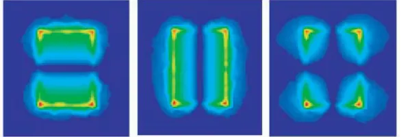
Figure 1. Normalized electric field magnitude maps of first three modes.
Figure 2. Convergence of complex resonant frequency of the first mode.
3. ADOPTED ANTENNA MODELING AND INPUT IMPEDANCE CALCULATIONS
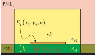
Let us consider a randomly shaped antenna having an axis aligned with the z-axis and placed on top of a PCB with relative permittivity εr. Let us also assume that the antenna will be probe-fed. So the target here is evaluate the input impedance at some arbitrary feed locations without having to undergo multiple full-wave driven simulations (to find the best feed location from an impedance point of view). The setup for a numerical Eigen problem would take the form shown in Fig. 3, but without any feed-specific model. The Eigen fields would then occupy all the space surrounding the antenna (reflecting all possible fringing fields). To utilize the modal data in calculating the input impedance, one needs to evaluate:
Zin(x0, y0, z0 =h) = Vin
(x0, y0, z0 =h)
Iin(x0, y0, z0=h) =
−h 0
Ez(x0, y0, z)dz
J(x0, y0, z0 =h)ds (1)
The electric field between the top antenna metalization and the ground plane may then be expanded using the Eigen field functions as [24, 25]:
Ez(x, y, z) =jωμ
p 1
k2−k2
p
J, ψp
ψp, ψpψp
(x, y, z) (2)
where
J, ψp=
Jψp∗dv (3)
and
ψp, ψp=
ψpψp∗dv (4)
formulations, the surface and volume integrals are written in a compact format for simplicity. In terms of the complex resonance frequency, the electric field at the source location may be re-written as:
Ez(x0, y0, z0) =jω
p 1
ε
1
ω2−ω2
p
J, ψp
ψp, ψpψp
(x0, y0, z0) (5)
As discussed earlier, the complex resonant frequency and the normalized field distribution are direct outcomes of any FEM Eigen mode solver. Thus, the field normalization process can be easily carried out as a post-processing numerical integration step. Hence, one can write:
Zin(x0, y0, z0 =h) =−jωh2
p 1
ω2−ω2
p
ψ∗p(x0, y0, z0 =h)
ε ψpψp∗dv
ψp(x0, y0, z0 =h) (6)
The input impedance can then be re-written in an expandable form of a parallel RLC circuit as:
Zin(x0, y0, z0) =−j 1
ωCdc −jω
p
1
Cp(x0, y0, z0) 1
ω2−ω2
p
(7)
whereCdc denotes the dccapacitance of the patch (DC mode), and
1
Cp(x0, y0, z0)
= h2ψ
∗
p(x0, y0, z0)ψp(x0, y0, z0)
εψpψ∗pdv
(8)
Rp(x0, y0, z0) =
Qradp0 ωp0Cp(x0, y0, z0)
(9)
Lp(x0, y0, z0) =
1
ω2p0Cp(x0, y0, z0)
(10)
with
ωp0=
(Re (ωp))2+ (Im (ωp))2 (11)
and
Qradp0 =
1 2
(Re (ωp))2+ (Im (ωp))2
Im (ωp)
(12)
The generalized equivalent circuit for a multimode radiator can then be developed, as in Fig. 4. It should be noted that an additional inductance is added to account for the inductance associated with probe feeding. Cdc is the dc capacitance, where its associated loss is typically ignored when using low-loss substrate materials. The RPLPCP circuit represents the fundamental antenna mode, with
RpLpCp representing the higher order modes taken into consideration. The term L is associated with an approximation for the effect of the higher order modes that are not considered in detailed analysis.
Figure 3. Setup for the Eigen problem. Outer cavity bounded with PEC walls.
Figure 4. Equivalent circuit for multimode radiator.
4. THE CONCEPT OF IMPEDANCE MAPS
A close look at (7) suggests the possibility of creating a map of the input impedance at each point of an antenna surface when fed by a probe. The ability of creating such maps is of great importance. Traditional techniques involve a large number of parametric trials and optimization cycles until a desired feed resistance is found. With the proposed concept, it is shown that seeking a location with specific input resistance is reduced to a single Eigen mode simulation and some simple field processing procedures.
Before being able to construct the impedance response (following Fig. 4), one first needs to account for the feeding mechanism. Proximity coupling and aperture feeding are among the possible schemes [15, 18–20, 33–35]. Here, the probe-feeding mechanism is chosen as an example for discussion. For most typical probe-fed antennas, the probe can be modeled with an inductance, Lprobe. There are several papers on the modeling of such an inductance [36].
To illustrate the proposed concept of impedance maps, two examples may be used. First, an E-Slot antenna [37–39] is analyzed through the modal solver. By analyzing its first two fundamental modes, it is possible to create the associated resistance maps. These are then used to find proper feed locations to have dual-feed dual-band antenna, as well as a single-feed dual-band antenna. Second, a very simple 3D conformal antenna, suitable for operation in a portable device at the GSM low band, is presented. The concept of impedance maps is then demonstrated by facilitating the determination of an appropriate feeding location.
4.1. Dual-Band Single-Feed and Dual-Feed Dual-Band Antenna Designs
An E-Slot antenna [38, 39] is widely known in the antenna community. It is simply a patch antenna with two slots forming the shape of the letter “E”. It is usually used to realize two close resonances and thus meet a wider bandwidth requirement, which is not achievable with a simple patch of the
Figure 7. Electric field distribution of the first fundamental mode.
Figure 8. Electric field distribution of the second fundamental mode.
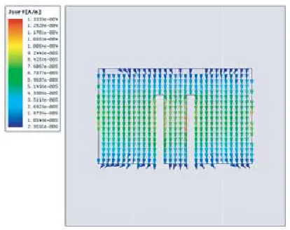
Figure 9. Surface current distribution of the first fundamental mode.
Figure 10. Surface current distribution of the second fundamental mode.
same dimensions. Also, it is sometimes used to create two resonances apart, to meet some dual band requirement. The latter application will be studied here. Let us arbitrarily choose the following values for the parameters shown in Fig. 5: L= 65, W = 105, W1 = 15.3, W2 = 6.3,Ls = 47, and H= 3 mm on a foam substrate. An Eigen mode simulation is applied seeking the first two fundamental modes of such patch.
Figure 6 shows a screen capture of the Eigen solver report solved in HFSS, and processed in Matlab, with Fig. 7–Fig. 10 illustrating the resulting modal electric field and surface current distributions of both modes.
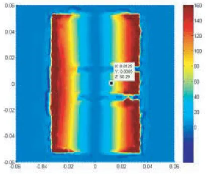
Now, using the resulting information from the Eigen solver and processing it using (7), one can plot the resistance values at any location on the patch surface, without the need for excessive parametric procedures. Fig. 11 and Fig. 12 show the resulting maps for each of the modes, respectively. For comparison, Fig. 13 compares the normalized input resistance across the center line of the E-patch at 2.05 GHz (when generated using an actual feeding probe through driven simulations) versus that predicted from the map. A very good correlation is observed. As noted in Fig. 11 and Fig. 12, there are a number of separate feed locations that can each excite one of the modes, while slightly perturbing the other. By placing two physical feed probes at the locations highlighted in Fig. 11 and Fig. 12, one realizes a dual-band dual-feed antenna with its response verified through a single driven numerical simulation, as shown in Fig. 14.
Figure 11. The resulting resistance map for the first mode with a feed location suitable for dual feed operation.
Figure 12. The resulting resistance map for the second mode with a feed location suitable for dual feed operation.
Figure 13. Comparing the normalized input resistance from driven and modal simulations.
Figure 14. Resulting response of the dual-band dual-feed antenna.
Figure 15. The resulting resistance map for the first mode with a feed location suitable for single feed operation.
Figure 17. Comparing the input return loss from the circuit model and the actual simulation.
simultaneously. Fig. 15 and Fig. 16 highlight one possible location. Using the modal analysis information, it is possible to predict the return loss plot of such single-feed dual band antenna. Fig. 17 compares the resulting return loss plot using the Eigen mode analysis with that from a single driven simulation with an actual feed placed at the location shown in Fig. 15. It is noteworthy to observe that the deviation seen in Fig. 17 may be attributed to two important factors. First, only the first two modes were utilized in (7). Adding more modes would increase the accuracy of the model, at the expense of more computational complexity. Second, placing the feed probe near the corner of the patch implies some inaccuracy in the utilized probe formulation (as discussed in Section 5.6).
4.2. Design of a Smartphone Antenna
The previous example featured a planar antenna. To verify the usefulness and the generality of the proposed modal analysis approach, this example discusses the design of a conformal 3D cell phone antenna. Even more complex variants of this design [40] can be studied using the same methodology. For simplicity, let’s focus on a design that meets the requirements for the 900 MHz cellphone band. Simple estimations using theQ-BW relations [41, 42] indicate that we need a Qof around 11 to cover GSM900 band with VSWR of 3.
For a smartphone board of 45×90 mm, one may use a simple strip wrapped around the edge of the board, as shown in Fig. 18 (details showing the steps to achieve such shape are beyond the scope of this paper. It mainly follows the routine presented in [43]). The wrapped strip has an overall height of 4 mm and is connected to the board through a short strip connection. The exact dimensions are determined from an Eigen mode simulation that searches for the required complex frequency to meet the bandwidth requirements. After some parametric trials, it is possible to have a design with modal data, as shown in Fig. 19. Here, the first fundamental radiating mode of the antenna is numbered as Mode 2. Its quality factor is around 9.6, which ensures meeting the required impedance bandwidth. It is worth mentioning that Mode 1 in Fig. 19 denotes a non-radiating numerical artifact mode associated with the perfect matching layers that terminate the space around the cell board.
Once a satisfactoryQis realized at the desired resonance frequency, the field data associated with
Figure 18. Visualization of a simple smartphone antenna.
Figure 20. Impedance (resistance) map of the smartphone antenna.
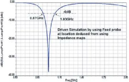
Figure 21. Input reflection coefficient of the antenna using a driven simulation.
Figure 22. The resistance map at (x, y) = (45,−14).
Figure 23. The resistance map at (x, y) = (45,−2).
Figure 24. Input resistance plots generated using a driven simulation with a probe located at different locations across they-axis.
the simulated structure is processed and the impedance (resistance) maps are generated (see Fig. 20). Studying these maps, one can rapidly find a suitable location for the feeding probe. Fig. 21 shows the resulting return loss from a numerical driven simulation of the cell antenna. It can be seen that the required bandwidth was successfully covered.
This is an acceptable accuracy, considering that the resistance maps were generated for only the first fundamental radiating mode. Including a few more additional modes should enhance the accuracy at the expense of more computational efforts.
5. APPLICATION IN TUNABLE ANTENNA DESIGN
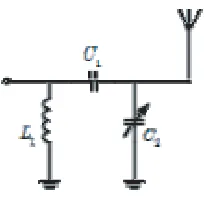
Let us consider a probe-fed patch antenna design of 60×40 mm, on a 3 mm foam layer over a large ground plane. The dominant radiation mode of the antenna resonates at 2.16 GHz. Let us further assume that the antenna shape has to be fixed, while meeting a VSWR = 2 : 1 or better from 1.9 GHz to 2.1 GHz. A look at the antenna scattering parameters using a probe 5 mm off-center of the patch’s long edge, and using the aforementioned Q calculations, it becomes clear that no RLC matching network exists to enable meeting the requisite bandwidth. One alternative is to use a tunable matching network. One realization for this network is shown in Fig. 26, where L1 = 22 [nH], C1 = 1 [pF], and C2 varies from 1 [pF] to 4 [pF]. Variable capacitors are widely available in various technologies, such as MEMS, BST or Silicon. Unfortunately, there is no such thing as ideal components, and all inductors and capacitors will have an associated Q value. When dealing with portable devices, one is typically bounded by surface mount devices (SMDs) to keep the circuit footprint as small as possible. The inductor Q of the 0402 family is typically less than 15, with slightly better numbers for the capacitors [44]. The Q
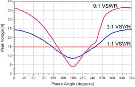
numbers are even worse for smaller families as the 0201. Currently, higher Q values are possible, but with a significant markup on price [44]. Thus, when considering the component losses in the matching network, and assuming a Q of 20 for the inductors and Q of 25 for the capacitors, the overall system efficiency (match+antenna) would range from 70% to 80% across 1.9 GHz to 2.1 GHz instead of the near 100% efficiency for a metal-based naturally-matched resonant patch antenna on a foam substrate. Another critical issue associated with matching networks is the ability to withstand high peak RF voltages when the load is in a high VSWR scenario. For example, let us consider feeding the aforementioned antenna when matched with the circuit in Fig. 26, using a 34 dBm signal (a typical value in cellphone applications). Let us also assume using a silicon-based solution, as that from Peregrine Semiconductor. The peak RF voltage rating of such a tunable capacitor is typically much less than 30 V. Interestingly, a quick calculation of the RF voltages across C2 for different load conditions reveals that the capacitor may in fact suffer from much higher voltages (Fig. 27, courtesy of Peregrine Semiconductor [46]). This is quite a serious issue that limits the practical application of the tunable capacitor concept in many applications.
Let us now consider an alternate solution by connecting the tunable capacitor directly to the antenna metallization. This topology is widely adopted in reconfigurable antenna solutions [45]. Here,
Figure 25. Scattering parameters of the probe-fed patch antenna.
Figure 27. RF voltages across the tunable capacitor in the matching network under study (courtesy of Peregrine Semiconductor).
Figure 28. Probe-fed patch antenna loaded with a tunable capacitor.
Figure 29. The variation in the input reflection coefficient of the antenna for different capacitor values.
the Eigen mode analysis discussed earlier can be applied to find the optimum location and value of the tunable element, in order to cover the desired range of frequencies. A capacitor Qof 25 was used in all numerical simulations. It was found that placing the capacitor 10 mm off-center across the long edge of the patch antenna would suffice. It is important to note that placing the capacitor directly at the edge would result in a wider tuning range at the expense of lower antenna efficiency. Fig. 28 shows a pictorial of the probe-fed antenna when loaded with a tunable capacitor at 10 mm off-center (probe placed 15 mm apart from capacitor). Fig. 29 demonstrates the tuning range of the antenna. A full-wave simulation reveals that the antenna has an overall efficiency of 90% or higher for all tuning states. In addition, the peak RF voltage remains below 17 V in all cases. This example shows the versatility of the Eigen mode method in tackling tunable-based designs. It also demonstrates that loading the antenna with the tunable element has some system advantages compared to relying on a tunable matching network.
6. DISCUSSION AND CONCLUSIONS
In this paper, the modal theory of antennas was re-visited. Through some basic analysis, a number of limitations with the commonly used formulations were highlighted. Some subtle changes were proposed to increase the range of validity and improve the accuracy of the relevant formulations. Through these formulations, the designer will always have relevant information about the maximum attainable bandwidth, the operational frequency, and the radiation pattern of any antenna at hand.
design tool through a number of design examples. This is a special concept that allows the designer to predict beforehand the impedance values at any location on a general antenna, without need for parametric and optimization trials seeking an appropriate feed location. Notably, the presented implementation steps are quite general and can be easily used towards the design of band multi-feed antennas.
Notably, there is a major challenge with the outlined design procedure. Specifically, there is still no systematic approach to find an antenna structure with the required complex frequency needed to meet the design specifications. To search for such a design, an efficient optimization strategy is needed. One should note that this optimization cycle is expected to be different from the traditional ones, given the presented advancements in the calculation of the antenna quality factor. An enhanced optimization cycle would then translate the return loss specifications into seeking structures with specific resonant frequencies and quality factors. This translation would provide the optimizer with some physics-based knowledge of the structure investigated, which in turn should improve the convergence of the optimization cycle.
REFERENCES
1. Cameron, R. J., C. M. Kudsia, and R. R. Mansour,Microwave Filters for Communication Systems: Fundamentals, Design, and Applications, Wiley-Interscience, 2007.
2. Lo, Y. T., D. Solomon, and W. F. Richards, “Theory and experiment on microstrip antennas,”
IEEE Transactions on Antennas and Propagation, Vol. 27, No. 2, 137–145, Mar. 1979.
3. Harrington, R. and J. Mautz, “Theory of characteristic modes for conducting bodies,” IEEE Transactions on Antennas and Propagation, Vol. 19, No. 5, 622–628, Sep. 1971.
4. Shen, Z. and R. Macphie, “Rigorous evaluation of the input impedance of a sleeve monopole by modal-expansion method,” IEEE Transactions on Antennas and Propagation, Vol. 44, 1584–1591, Dec. 1996.
5. Deschamps, A., “Microstrip microwave antennas,”US-AF Symposium on Antennas, 1953.
6. Derneryd, G., “A theoretical investigation of the rectangular microstrip antenna element,” IEEE Transactions on Antennas and Propagation, Vol. 26, No. 4, 532–535, Jul. 1978.
7. Carver, R., “A modal expansion theory for the microstrip antenna,” IEEE Antennas and Propagation Symposium, 101–104, Jun. 1979.
8. Richards, W. F., Y. T. Lo, and D. D. Harrison, “An improved theory of microstrip antennas and applications,”IEEE Transactions on Antennas and Propagation, Vol. 27, No. 6, 853–858, Nov. 1979. 9. Carver, K. R., “Practical analytical techniques for the microstrip antenna,” Workshop on Printed
Circuit Antenna Technology, 1–20, New Mexico State University, Oct. 1979.
10. Hammerstad, E. O., “Equations for microstrip circuit design,” European Microwave Conference, 268–272, Sep. 1975.
11. Carver, K. R. and J. W. Mink, “Microstrip antenna technology,” IEEE Transactions on Antennas and Propagation, Vol. 29, No. 1, 2–24, Jan. 1981.
12. Schaubert, H., F. G. Farar, A. Sindoris, and S. T. Hayes, “Microstrip antennas with frequency agility and polarization diversity,”IEEE Transactions on Antennas and Propagation, Vol. 29, No. 1, 118–123, Jan. 1981.
13. Bhartia, P. and I. J. Bahl, “Frequency agile microstrip antennas,” Microwave Journal, 67–60, Oct. 1982.
14. Richards, W. F. and Y. T. Lo, “Theoretical and experimental investigation of a microstrip radiator with multiple limped linear loads,” Electromagnetics, Vol. 3, Nos. 3–4, 371–384, Jul.–Dec. 1983. 15. Richards, W. F., “Microstrip antennas,” Antenna Handbook: Theory, Applications and Design,
Chapter 10, Van Nostrand Reinhold Co., New York, 1988.
16. Schaubert, H., D. M. Pozar, and A. Adrian, “Effect of microstrip antenna substrate thickness and permittivity: Comparison of theories and experiment,” IEEE Transactions on Antennas and Propagation, Vol. 37, No. 6, 667–682, Jun. 1989.
23. Wong, K. L.,Planar Antennas for Wireless Communications, Wiley-Interscience, 2003. 24. Harrington, R. F., Time Harmonic Electromagnetic Fields, McGraw Hill, New York, 1961. 25. Collin, R. E.,Field Theory of Guided Waves, McGraw Hill, New York, 1960.
26. Stuart, R., “Eigenmode analysis of small multielement spherical antennas,”IEEE Transactions on Antennas and Propagation, Vol. 56, No. 9, 2841–2851, Sep. 2008.
27. Stuart, R., “Eigenmode analysis of a two element segmented capped monopole antenna,” IEEE Transactions on Antennas and Propagation, Vol. 57, No. 10, 2980–2988, Oct. 2009.
28. Ansoft HFSS v11.0, Ansoft, LLC, 2008, [Online], available: www.ansoft.com/products/hf/hfss/. 29. COMSOL MULTIPHYSICS v3.4, COMSOL Group, 2008, [Online], available: www.comsol.com. 30. Matlab Antenna Toolbox, Open Source, [Online], available: http://ece.wpi.edu/mom/.
31. Sacks, Z. S., D. M. Kingsland, R. Lee, and J. F. Lee, “A perfectly matched anisotropic absorber for use as an absorbing boundary condition,” IEEE Transactions on Antennas and Propagation, Vol. 43, No. 12, 1460–1463, 1995.
32. Chew, W. C. and W. H. Weedon, “A 3D perfectly matched medium from modified Maxwell’s equations with stretched coordinates,” Micro. Opt. Tech. Lett., Vol. 7, 599–604, 1994.
33. Bahl, J. J. and P. Bhartia, Microstrip Antennas, Artech House, 1980.
34. James, J. R., P. S. Hall, and C. Wood, “Microstrip antenna,” P. Peregrinus on behalf of the Institution of Electrical Engineers, 1981.
35. Garg, R., P. Bhartia, I. Bahl, and A. Ittipiboon, Microstrip Antenna Design Handbook, Artech House, Norwood, 2001.
36. Hao, X., D. R. Jackson, and J. T. Williams, “Comparison of models for the probe inductance of a parallel-plate waveguide and a microstrip patch,”IEEE Transactions on Antennas and Propagation, Vol. 53, No. 10, 3229–3235, Oct. 2005.
37. Shaker, G., S. Safavi-Naeini, N. Sangary, and M. Bakr, “A generalized modal analysis method for antenna design,”IEEE International Symposium on Antennas and Propagation Techniques, 2009. 38. Kumar, G. and K. P. Ray, Broadband Microstrip Antennas, Artech House, Norwood, MA, 2003. 39. Yang, F. and Y. Rahmat-Samii, “Wide-band E-shaped patch antennas for wireless
communica-tions,” IEEE Transactions on Antennas and Propagation, Vol. 49, No. 7, 1094–1100, Jul. 2001. 40. Shaker, G. and S. Safavi-Naeini, “Highly miniaturized fractal antennas,”IEEE Radio and Wireless
Symposium, 2007.
41. Yaghjian, A. D. and S. R. Best, “Impedance, bandwidth, andQ of antennas,” IEEE Transactions on Antennas and Propagation, Vol. 53, No. 4, 1298–1324, Apr. 2005.
42. Shaker, G., S. Safavi-Naeini, G. Rafi, and N. Sangary, “On the fundamentalQ-bandwidth relations for antennas,”IEEE Antennas and Propagation Symposium, Jul. 2008.
43. Shaker, G., M. H. Bakr, N. Sangary, and S. Safavi-Naeini, “Accelerated antenna design methodology exploiting parameterized cauchy models,” Progress In Electromagnetic Research B, Vol. 18, 279–309, 2009.
44. Murata Manufacturing Co. Ltd., http://www.murata.com.