WAVEGUIDE SIMULATION USING THE HIGH-ORDER SYMPLECTIC FINITE-DIFFERENCE TIME-DOMAIN SCHEME
W. Sha
Department of Electrical and Electronic Engineering University of Hong Kong
Pokfulam Road, Hong Kong, China
X. L. Wu and Z. X. Huang
Key Laboratory of Intelligent Computing & Signal Processing Anhui University
Feixi Road 3, Hefei 230039, China
M. S. Chen
Department of Physics and Electronic Engineering Hefei Teachers College
Jinzhai Road 327, Hefei 230061, China
Abstract—The high-order symplectic finite-difference time-domain scheme is applied to modeling and simulation of waveguide structures. First, the perfect electric conductor boundary is treated by the image theory. Second, to excite all possible modes, an efficient source excitation method is proposed. Third, the modified perfectly matched layer is extended to its high-order form for absorbing the evanescent waves. Finally, a high-order scattering parameter extraction technique is developed. The cases of waveguide resonator, waveguide discontinuities, and periodic waveguide structure demonstrate that the high-order symplectic finite-difference time-domain scheme can obtain better numerical results than the traditional finite-difference time-domain method and save computer resources.
1. INTRODUCTION
As the most standard algorithm, the traditional finite-difference time-domain (FDTD) method [1, 2], which is explicit and second-order accurate in both space and time, has been widely applied to modeling and simulation of waveguide structures [3–11]. However, the numerical dispersion in the traditional FDTD method leads to less efficiency for solving the closed problems. Furthermore, waveguide simulations always consume longer CPU time compared with the same-sized scattering problems. Hence, the numerical results by the traditional FDTD method will suffer from significant accumulated errors.
To reduce the numerical dispersion in the traditional FDTD method, a variety of spatial high-order approaches, such as high-order FDTD [12, 13], multi-resolution time-domain [14, 15], and discrete singular convolution [16] methods, are proposed and their applications in waveguide simulation are developed. For the high-order approaches, there are still some problems left to be solved. On the one hand, the image theory uses the stair-cased model, which is inaccurate for treating the curved dielectric and conducting boundaries. On the other hand, the required high-order techniques for source excitation, absorbing boundary condition, and wide-band scattering parameter extraction are seldom reported.
Focusing on these points, we apply the high-order symplectic finite-difference time-domain (SFDTD) scheme to analyze the three-dimensional guided-wave problems. For the time direction, different from the five-stage fourth-order symplectic integrators used in [16, 17], the three-stage third-order symplectic integrators [18] are employed to achieve lower computational complexity. For the spatial direction, the fourth-order staggered difference with Yee lattice is used. Moreover, the required high-order techniques matched the SFDTD(3,4) scheme are developed.
2. THEORY
2.1. Formulation
A function of space and time evaluated at a discrete point in the Cartesian lattice and at a discrete stage in the time step can be written as
F(x, y, z, t) =Fn+l/mi∆x, j∆y, k∆z,(n+τl) ∆t
(1)
where ∆x, ∆y, and ∆z are, respectively, the lattice space steps in the
x,y, andz coordinate directions, ∆tis the time step,i,j,k,n,l, and
the total stage number, andτl is the fixed time with respect to thelth
stage.
For the spatial direction, the explicit and fourth-order-accurate staggered difference in conjugation with the Yee lattice is used to discretize the first-order spatial derivative
∂Fn+l/m
∂δ
!
h
≈ 98 ×F
n+l/m(h+ 1/2)−Fn+l/m(h−1/2)
∆δ
−241 ×F
n+l/m(h+ 3/2)−Fn+l/m(h−3/2)
∆δ
(2)
whereδ =x, y, z and h=i, j, k.
For the time direction, Maxwell’s equations in homogeneous, lossless, and sourceless media can be written as [17]
∂ ∂t
H E
= (U +V)
H E
(3)
U =
{0}3×3 −µ−1ℜ3×3
{0}3×3 {0}3×3
, V =
{0}3×3 {0}3×3
ε−1ℜ
3×3 {0}3×3
(4)
ℜ3×3 =
0 −∂z∂ ∂y∂
∂
∂z 0 −∂x∂
−∂y∂ ∂x∂ 0
(5)
where H is the vector magnetic field, E is the vector electric field, {0}3×3 is the 3×3 null matrix,ℜis the three-dimensional curl operator,
and εandµ are the permittivity and permeability of the media. Using the product of elementary symplectic mapping, the exact solution of (3) can be approximated by the m-stage p-th symplectic integration scheme [19]
exp
∆t(U +V)
=
m Y
l=1
exp(dl∆tV) exp (cl∆tU) +O
∆pt+1
≈
m Y
l=1
(I+dl∆tV) (I+cl∆tU) (6)
where cl and dl are the symplectic integrators. To lower the
6 7 8 9 10 11 12 13 −90
−80 −70 −60 −50 −40 −30
PPW
Relative Phase Vel
ocity Error
(dB
)
FDTD(2,4) SFDTD(3,4)
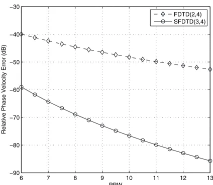
Figure 1. Dispersion curves for a plane wave traveling at θ = 60◦
and φ = 30◦ versus points per wavelength (PPW) discretization:
CFL = 0.495.
withm= 3,c1 = 0.26833010,c2 =−0.18799162, andc3= 0.91966152.
Compared with the Runge-Kutta method, the symplectic integration scheme can save considerable memory and conserves the symplectic structure of electromagnetic field [20].
As a result, the SFDTD(3,4) scheme is constructed. The Courant-Friedrichs-Levy (CFL) number of the SFDTD(3,4) scheme is 1.118, which is bigger than 0.743 for the SFDTD(4,4) scheme proposed in [17]. In each time step, the SFDTD(3,4) scheme only requires three stages compared with five stages for the SFDTD(4,4) scheme. Hence, considerable CPU time will be saved by the three-stage third-order symplectic integrators. Figure 1 gives the relative phase velocity error as a function of points per wavelength (PPW) for a plane wave traveling at θ = 60◦ and φ= 30◦. The CFL number is set to be 0.495 that is
the stability limit of the FDTD(2,4) approach [13]. From Fig. 1, we can see that the SFDTD(3,4) scheme is superior to the FDTD(2,4) approach.
p
ε0/µ0Ex) can be derived as follows
ˆ Exn+l/m
i+1 2, j, k
= ˆExn+(l−1)/m
i+ 1 2, j, k
+ 1
εr i+12, j, k
×
+αy1×
Hzn+l/m
i+1 2, j+
1 2, k
−Hzn+l/m
i+1 2, j−
1 2, k
−αz1×
Hyn+l/m
i+ 1 2, j, k+
1 2
−Hyn+l/m
i+ 1 2, j, k−
1 2
+αy2×
Hzn+l/m
i+1 2, j+
3 2, k
−Hzn+l/m
i+1 2, j−
3 2, k
−αz2×
Hyn+l/m
i+1 2, j, k+
3 2
−Hyn+l/m
i+ 1 2, j, k−
3 2
(7)
αy1 =
9
8dl×CFLy, αz1 = 9
8dl×CFLz (8a)
αy2 = −
1
24dl×CFLy, αz2= −1
24dl×CFLz (8b) CFLy =
1 õ
0ε0
∆t
∆y
, CFLz =
1 õ
0ε0
∆t
∆z
(9)
where ε0 and µ0 are the permittivity and permeability of free space,
andεr is the relative permittivity of the media. For the uniform space
step, ∆x= ∆y = ∆z = ∆δ.
2.2. Boundary Treatment
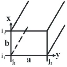
Figure 2 shows a rectangular waveguide with size of a × b. For the propagating modes, the electromagnetic waves travel along the z direction.
Similar to the original operation [15, 16], the image theory is used for treating the perfect electric conductor boundary.
Take the conducting plane of i = i1 for example, the tangential
electric field components outside the waveguide are obtained by the anti-symmetric extensions
ˆ Ey
i1−1, j+
1 2, k
=−Eˆy
i1+ 1, j+
1 2, k
, j1 ≤j≤j2−1 (10)
ˆ Ez
i1−1, j, k+
1 2
=−Eˆz
i1+ 1, j, k+
1 2
, j1 ≤j≤j2 (11)
Similarly, the tangential magnetic field components are obtained by the symmetric extensions
Hy
i1−
1 2, j, k+
1 2
= Hy
i1+
1 2, j, k+
1 2
, j1 ≤j≤j2 (12)
Hy
i1−
3 2, j, k+
1 2
= Hy
i1+
3 2, j, k+
1 2
, j1 ≤j≤j2 (13)
Hz
i1−
1 2, j+
1 2, k
= Hz
i1+
1 2, j+
1 2, k
, j1 ≤j ≤j2−1 (14)
Hz
i1−
3 2, j+
1 2, k
= Hz
i1+
3 2, j+
1 2, k
, j1 ≤j ≤j2−1 (15)
In addition, the high-order subcell strategy [21] is employed to model the material discontinuities. The strategy is compatible with the spatial fourth-order differences and can get the averaged permittivities at the dielectric-dielectric interface. The relevant theory and numerical results have been reported in [21].
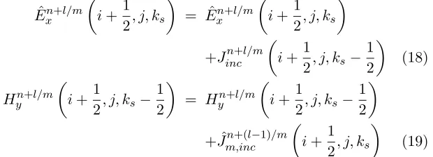
2.3. Source Excitation
To excite the resonant modes, the initial conditions of the longitudinal fields are
Hz0
i+1 2, j+
1 2, k
= exp
"
− i+
1 2−ic
2
+ j+12 −jc2
2τ2
g
#
(16)
ˆ Ez0
i, j, k+1 2
= exp
"
−(i−ic)
2
+ (j−jc)2
2τ2
g
#
(17)
whereic,jc, andkc are the grid indexes of waveguide center, andτg is
To excite the propagating modes, the magnetic field source (electric current) and the electric field source (magnetic current) are respectively given by
ˆ Exn+l/m
i+ 1 2, j, ks
= ˆExn+l/m
i+1 2, j, ks
+Jincn+l/m
i+1
2, j, ks− 1 2
(18)
Hyn+l/m
i+1
2, j, ks− 1 2
= Hyn+l/m
i+1
2, j, ks− 1 2
+ ˆJm,incn+(l−1)/m
i+ 1 2, j, ks
(19)
where i1 ≤ i ≤ i2 −1, j1 ≤ j ≤ j2, and ks is the source plane as
shown in Fig. 3. In previous work, the magnetic field source was used extensively. Although the magnetic field source can excite the dominant TE10 mode, it can not excite some TM modes properly.
Similarly, the electric field source can not excite the TE modes. Hence, we must employ (18) and (19) simultaneously.
Both the magnetic and electric field sources can be written as
Π(t, x, y) =ζ(t)·ϑ(x, y), Π =Jinc,Jˆm,inc (20)
whereζ(t) is the cosine-modulated Gaussian pulse ζ(t) =−cos(ωt) exp
−4π(t−T0)
2
W2
(21)
Figure 3. The side view of the rectangular waveguide. The source excitation is added at the plane ofk=ks, and the scattering parameter
( ˜S11 parameter) can be extracted at the plane ofk=kr. The first and
and its effective frequency range is [ω/2π−2/W, ω/2π+ 2/W]. The functionϑ(x, y) depends on the distribution of transverse fields, i.e.,
ϑ(x, y) =X
m X
n
sinmπy a
cosnπx b
(22)
For the dominant TE10mode, m= 1 and n= 0.
2.4. Modified Perfectly Matched Layer
In view of the spatial fourth-order differences used in the non-PML regions, the low-order perfectly matched layer (PML) using second-order differences will lead to the fictitious (non-physical) reflection at the media-layer interface. So, the modified perfectly matched layer (MPML) [22], which can absorb the evanescent waves, should be extended to its high-order form.
Using the split-field technique, the x component of the scaled electric field can be split into two subcomponents
ˆ
Ex = ˆExy+ ˆExz (23)
The update equation of the subcomponent ˆExy can be given by
ˆ Exyn+l/m
i+1 2, j, k
= ˆExyn+(l−1)/m
i+1 2, j, k
+ 1
εr i+12, j, k
×
+αy1×
Hzn+l/m
i+1 2, j+
1 2, k
−Hzn+l/m
i+ 1 2, j−
1 2, k
+αy2×
Hzn+l/m
i+1 2, j+
3 2, k
−Hzn+l/m
i+1 2, j−
3 2, k
(24)
One can see that there is no modified perfectly matched layer in the y direction. For the z direction, the update equation of the subcomponent ˆExz is
ˆ Enxz+l/m
i+ 1 2, j, k
= exp (−ξ)×Eˆxzn+(l−1)/m
i+1 2, j, k
+1−exp (−ξ)
ξ ×
1
εpr,z i+12, j, k×
−αz1×
Hyn+l/m
i+1 2, j, k+
1 2
−Hyn+l/m
i+1 2, j, k−
1 2
−αz2×
Hyn+l/m
i+1 2, j, k+
3 2
−Hyn+l/m
i+1 2, j, k−
3 2
whereξ =dl∆tσzp(i+12, j, k)εpz(i+12, j, k) and εpz=ε0εpr,z.
The electric conductivities and the relative permittivities in the modified perfectly matched layer can be set as
σzp(Λ) = σzpmax
Λ Γ
κ
(26)
εpr,z(Λ) = εr·
1 +εpr,zmax
Λ Γ
κ
(27)
where Γ is the layer thickness, Λ is the distance from the media-layer interface, and κ is the polynomial order. According to our numerical results, κ= 3 can achieve the best absorbing effect. The maximum of the electric conductivities is given by
σzpmax= 5×10
−4
õ
rεr∆z
(28)
and that of the relative permittivities is given by 5 ≤ εpr,zmax ≤ 10.
In addition, (26) and (27) also suit the settings of the magnetic conductivities and the relative permeabilities in the modified perfectly matched layer.
2.5. Parameter Extraction
For the eigenvalue analysis of waveguide, one can find the cut-off and resonant frequencies by computing the total energy of the electric field in frequency-domain. For the cut-off frequency analysis, the waveguide is truncated by the modified perfectly matched layer and the total energy is of form
ΣS˜
E=
1 4
Z Z
S
εE˜ ·E˜†dS = 1 4 Z Z S ε E˜x
2 + E˜y
2 + E˜z
2
dS (29)
where ˜Eis the electric field in frequency-domain that can be obtained by the fast Fourier transform and S denotes the arbitrary transverse plane of the waveguide.
For the resonant frequency analysis, there is no absorbing boundary condition and the total energy for the waveguide resonator is
ΣV˜
E=
1 4
Z Z Z
V
εE˜ ·E˜†dV = 1 4
Z Z Z
V
ε
E˜x
2 + E˜y
2 + E˜z
2
For the computation of wide-band scattering parameter, the mode voltage and current can be defined as
˜ V =
Z Z
S h
˜
Et(x, y, zr)×h˜t,n(x, y) i
·dS (31) ˜
I =
Z Z
S h
˜
et,n(x, y)×H˜t(x, y, zr) i
·dS (32)
where ˜Et and ˜Ht are the transverse components of the electric and
magnetic fields, ˜et,n and ˜ht,n are the normalized transverse-field
components of thenth eigenfunction, andzr =kr∆zis thezcoordinate
of the scattering parameter extraction plane.
Using the differential method [11], the characteristic impedance of the waveguide can be defined as
˜ Z =
v u u u t
˜
V ·dV /dz˜ ˜
I ·dI/dz˜
(33)
To obtain the high-order accuracy, the variables of (33) can be discretized as follows
˜ V
z=zr
= ˜V(kr) (34)
˜ I
z=zr
≈ 169 ×hI(k˜ r+ 0.5) + ˜I(kr−0.5) i
−161 ×hI˜(kr+ 1.5) + ˜I(kr−1.5) i
(35)
dV˜ dz
z=zr
≈ 23×V˜(kr+ 1)∆−V˜(kr−1)
z
−121 ×V˜(kr+ 2)∆−V˜(kr−2)
z
(36)
dI˜ dz
z=zr ≈ 9
8× ˜
I(kr+ 0.5)−I(k˜ r−0.5)
∆z
−241 ×I˜(kr+ 1.5)∆−I(k˜ r−1.5)
z
(37)
waves are of the form
˜ Vinc =
˜
V + ˜Z·I˜ 2pZ˜
(38)
˜ Vref =
˜
V −Z˜·I˜ 2pZ˜
(39)
Hence, the reflection coefficient or ˜S11 parameter can be obtained by
˜ S11=
˜ Vref
˜ Vinc
(40)
3. NUMERICAL RESULTS
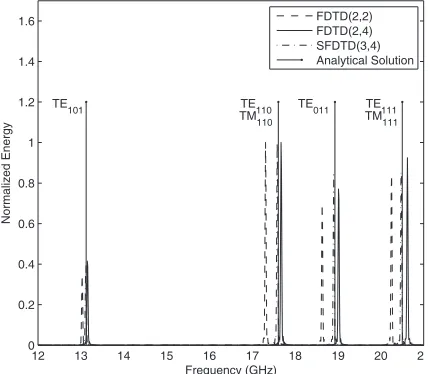
1. The resonant frequency analysis for rectangular waveguide cavity. The size of the waveguide resonator is a×b×c = 19.050 mm × 9.525 mm × 14.288 mm. Other parameters are taken as ∆δ =
2.381 mm, CFLδ = 0.4, and nmax = 10000. The frequency of
the cosine-modulated Gaussian pulse ranges form 12 GHz to 21 GHz. Within the frequency range, all possible resonant modes include TE101, TE110(TM110), TE011, and TE111(TM111). In particular, the
12 13 14 15 16 17 18 19 20 21
0 0.2 0.4 0.6 0.8 1 1.2 1.4 1.6
Frequency (GHz)
Normalized Energy
TE011
TE101 TE110
TM110 TMTE111111 FDTD(2,2) FDTD(2,4) SFDTD(3,4) Analytical Solution
perfect electric conductor boundary is treated by the image theory for the SFDTD(3,4) scheme. Using (30), the total energy of electric field in frequency-domain is computed. Figure 4 shows the curve of the normalized total energy and its peaks corresponding to the resonant frequencies. One can see that compared with the high-order FDTD(2,4) approach [13] and the traditional FDTD(2,2) method, the SFDTD(3,4) scheme can find the resonant frequencies better.
2. The cut-off frequency and scattering parameter analyses for dielectric-loaded waveguide. The WR-3 waveguide with size of 0.8636 mm×0.4318 mm is considered.
First, the different source excitation methods are compared for the cut-off frequency analysis. The settings are given as ∆δ = 0.072 mm
and CFLδ= 0.5, and the total energy of electric field is calculated by
(29). The frequency range of interest is [170 GHz,780 GHz]. If m ∈ [0,2] andn∈[0,2], all possible propagating modes include TE10, TE01,
TE20, TE11(TM11), TE21(TM21), TE12(TM12), and TE22(TM22). The
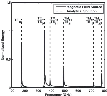
result only with the magnetic field source (18) is shown in Fig. 5, where TM11 and TM12 modes can not be excited properly. Likewise,
the result only with the electric field source (19) is shown in Fig. 6, where TE10, TE01, and TE20modes can not be excited. However, once
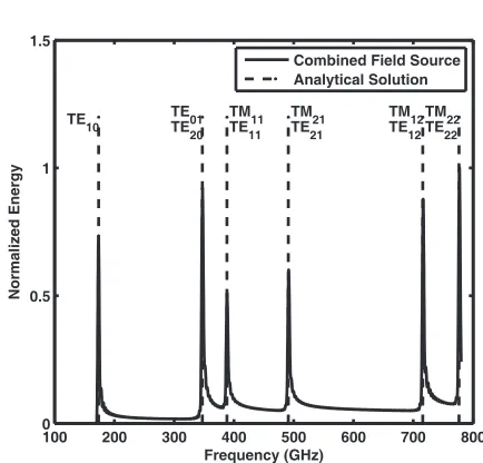
the magnetic field source is combined with the electric field source, all possible modes can be well excited as shown in Fig. 7.
100 200 300 400 500 600 700 800 0
0.5 1 1.5
Frequency (GHz)
Normalized Energy
TE
10 TE20
TE
01
TE11 TM
11
TE21 TM
21
TE12 TM
12
TE22 TM
22
Magnetic Field Source Analytical Solution
Second, we change the space step and the time step, then record the errors for the traditional FDTD(2,2) method and the SFDTD(3,4) scheme. The error can be defined as
η=
6 X
i=1
|fiana−finum| max
i f
ana i
(41)
where fiana and finum are the ith cut-off frequencies calculated by the analytical solution and the numerical method, respectively. From Table 1, for a given error bound 1%, the space step and the time
100 200 300 400 500 600 700 800 0
0.5 1 1.5
Frequency (GHz)
Normalized Energy
TE10 TE
20
TE01 TE11 TM11
TE21 TM21
TE12 TM12
TE22 TM22 Electric Field Source Analytical Solution
Figure 6. Electric field source excitation for computing the cut-off frequencies of the rectangular waveguide.
Table 1. The errors of the cut-off frequencies for the SFDTD(3,4) scheme and the traditional FDTD(2,2) method.
Method ∆δ CFLδ η
SFDTD(3,4) 0.072 mm 1.0 1.04%
SFDTD(3,4) 0.036 mm 1.0 0.19%
FDTD(2,2) 0.072 mm 0.5 6.61%
100 200 300 400 500 600 700 800 0
0.5 1 1.5
Frequency (GHz)
Normalized Energy
TE
10 TE
20
TE01 TE
11
TM11 TE
21
TM21
TE
12
TM12 TE
22
TM22 Combined Field Source Analytical Solution
Figure 7. Combined field source excitation for computing the cut-off frequencies of the rectangular waveguide.
step of the SFDTD(3,4) scheme are two times bigger than those of the traditional FDTD(2,2) method. The memory of a time-domain algorithm is proportional toO(1/∆3δ). According to the computational complexity analysis in [18], the total simulation time is proportional to O (1/∆4
δ)·(m/CFLδ)·(q)
, where m is the stage number and q is the order of spatial difference. For the traditional FDTD(2,2) method, m = 1 and q = 2. For the SFDTD(3,4) scheme, m = 3 and q = 4. As a result, the ratio of memory cost for the traditional FDTD(2,2) method and the SFDTD(3,4) scheme is 8 : 1. The ratio of CPU time for the traditional FDTD(2,2) method and the SFDTD(3,4) scheme is 16 : 3.
Third, the local reflection coefficients for both the perfectly matched layer and the modified perfectly matched layer are analyzed. Theεpr,zmaxfor the perfectly matched layer and the modified perfectly
matched layer are, respectively, 0 and 5. The total computational region occupies 6×12×31 grids and the record point is located at (3,6,19). The number of the absorbing boundary layer is 10; the space step is ∆δ = 0.072 mm; and the Courant-Friedrichs-Levy number is 1.0.
the vacuum-layer interface. Moreover, the local reflection coefficients can be defined as
ρ(n) = 20 log10
Eˆ
Ref
x (n)−EˆxN um(n)
max
n Eˆ
Ref
x (n)
(42)
0 50 100 150 200
−300 −250 −200 −150 −100 −50 0 50
Local Reflection Coefficients (dB)
Time Step (n)
High−Order MPML
High−Order PML Unstable
Figure 8. The local reflection coefficients of the high-order perfectly matched layer (PML) and the high-order modified perfectly matched layer (MPML).
where ˆExRef and ˆExN um are, respectively, the reference and numerical
solutions for the ˆExfield. Figure 8 shows the local reflection coefficients
as a function of time step. Although both the perfectly matched layer and the modified perfectly matched layer employ the split-field forms and are weakly well-posed [23], the modified perfectly matched layer can keep stable as the time step increases. It is noted that two symplectic integrators c2 and d2 are negative, hence the exponential
180 200 220 240 260 280 300 320 340 −40
−35 −30 −25 −20 −15 −10 −5 0 5
Frequency (GHz) |S11
| (dB)
FDTD(2,2) SFDTD(3,4) FEM
~
Figure 9. The scattering parameter of the dielectric-loaded waveguide. The solution by finite element method (FEM) is given as reference solution.
further test the stability of the modified perfectly matched layer, the program runs for 50000 time steps. We find the modified perfectly matched layer is still stable.
Finally, the waveguide discontinuities are simulated. Loaded with a dielectric square cylinder of relative permittivity 3.7 and of size 0.8636 mm ×0.4318 mm ×0.504 mm, the waveguide is driven in the TE10dominant-mode with frequency range of [180 GHz,340 GHz]. The
settings are taken as ∆δ = 0.056 mm, CFLδ = 0.5, andnmax= 10000.
For the traditional FDTD(2,2) method, the air-dielectric interface is modeled by the low-order subcell strategy [24] and the scattering parameter is extracted by the low-order differential method [11]. For the SFDTD(3,4) scheme, both the high-order subcell strategy [21] and the high-order differential method are employed. From Fig. 9, it can be clearly seen that the scattering parameter computed by the SFDTD(3,4) scheme agrees with the reference solution well.
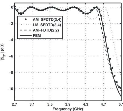
3. Computation of wide-band scattering parameter for periodic waveguide structure. Figure 10 shows the geometry of the structure. The space steps are set as ∆x×∆y×∆z = 14.542 mm×4.847 mm×
Figure 10. The geometry of the periodic waveguide structure. The size of the waveguide is a×b = 58.170 mm ×29.083 mm, and each dielectric cylinder with diameter of b/2, height of b, and relative permittivity of 2.1 is placed at an equidistance of b.
2.7 3.1 3.5 3.9 4.3 4.7 5.1 −10
−8 −6 −4 −2 0
Frequency (GHz)
|S21
| (dB)
AM−SFDTD(3,4) LM−SFDTD(3,4) AM−FDTD(2,2) FEM
~
scheme, the curved air-dielectric interface is treated by the local and averaged material models. The averaged material model uses the high-order subcell strategy [21]. For the traditional FDTD(2,2) method, the averaged material model uses the low-order subcell strategy [24]. Similar to the ˜S11 parameter, the ˜S21 parameter can be calculated by
(38)–(40) but should be extracted at the right hand of the waveguide. From Fig. 11, one can see that the averaged material model is superior to the local material model. Furthermore, the result by the traditional FDTD(2,2) method loses some accuracy when the frequency increases. The infinity-norm errors for the averaged-material-SFDTD(3,4), local-material-SFDTD(3,4), and averaged-material-FDTD(2,2) methods are 0.73, 5.03, and 1.20. The two-norm errors for the three methods are 1.84, 12.13, and 2.81.
4. CONCLUSION
The SFDTD(3,4) scheme, which is explicit, non-dissipate, and high-order-accurate, has been introduced to simulate the three-dimensional waveguide problems. A variety of techniques involving boundary treatment, source excitation, absorbing boundary condition, and scattering parameter extraction are developed to match the scheme. First, the image theory and the high-order subcell strategy are used respectively to treat the perfect electric conductor boundary and the dielectric-dielectric interface. Second, to excite all possible propagating modes, the combined source excitation is required. Third, the modified perfectly matched layer has good absorbing effect and keeps stable for long-term simulation. Finally, the scattering parameter can be extracted by running program once and is still accurate under coarse grid condition. With the aid of the techniques, the high-order SFDTD scheme can achieve high accuracy and save computer resources.
ACKNOWLEDGMENT
The first author expresses his sincere gratitude to Dr. Jie Xiong, University of Illinois at Urbana-Champaign, for improving the readability of the paper.
REFERENCES
1. Yee, K. S., “Numerical solution of initial boundary value problems involving Maxwell’s equations in isotropic media,” IEEE Trans.
2. Taflove, A., Computational Electrodynamics: The
Finite-difference Time-domain Method, Artech House, Norwood, MA,
1995.
3. Christ, A. and H. L. Hartnagel, “Three-dimensional finite-difference method for the analysis of microwave-device em-bedding,” IEEE Trans. on Microwave Theory and Techniques, Vol. 35, 688–696, 1987.
4. Chu, S. T., W. P. Huang, and S. K. Chaudhuri, “Simulation and analysis of wave-guide based optical integrated-circuits,”
Computer Physics Communications, Vol. 68, 451–484, Nov. 1991.
5. Krupezevic, D. V., V. J. Brankovic, and F. Arndt, “Wave-equation FD-TD method for the efficient eigenvalue analysis and S-matrix computation of waveguide structures,”IEEE Trans. on Microwave
Theory and Techniques, Vol. 41, 2109–2115, 1993.
6. Vielva, L. A., J. A. Pereda, A. Prieto, and A. Vegas, “FDTD multimode characterization of waveguide devices using absorbing boundary conditions for propagating and evanescent modes,”
IEEE Microwave and Guided Wave Letters, Vol. 4, 160–162, 1994.
7. Zhao, A. P. and A. V. Raisanen, “Application of a simple and efficient source excitation technique to the FDTD analysis of waveguide and microstrip circuits,” IEEE Trans. on Microwave
Theory and Techniques, Vol. 44, 1535–1539, 1996.
8. Shibata, T. and T. Itoh, “Generalized-scattering-matrix modeling of waveguide circuits using FDTD field simulations,”IEEE Trans.
on Microwave Theory and Techniques, Vol. 46, 1742–1751, 1998.
9. Gwarek, W. K. and M. Celuch-Marcysiak, “Wide-band S-parameter extraction from FD-TD simulations for propagating and evanescent modes in inhomogeneous guides,” IEEE Trans.
on Microwave Theory and Techniques, Vol. 51, 1920–1928, 2003.
10. Wang, S. and F. L. Teixeira, “An equivalent electric field source for wideband FDTD simulations of waveguide discontinuities,”
IEEE Microwave and Wireless Components Letters, Vol. 13, 27–
29, 2003.
11. Gwarek, W. K. and M. Celuch-Marcysiak, “Differential method of reflection coefficient extraction from FDTD simulations,”IEEE
Microwave and Guided Wave Letters, Vol. 6, 215–217, 1996.
12. Young, J. L., D. Gaitonde, and J. S. Shang, “Toward the construction of a fourth-order difference scheme for transient EM wave simulation: staggered grid approach,” IEEE Trans. on
Antennas and Propagation, Vol. 45, 1573–1580, Nov. 1997.
fourth-order accurate explicit finite difference scheme for the time-domain Maxwell’s equations,”Journal of Computational Physics, Vol. 168, 286–315, Apr. 2001.
14. Krumpholz, M. and L. P. B. Katehi, “MRTD: New time-domain schemes based on multiresolution analysis,” IEEE Trans. on
Microwave Theory and Techniques, Vol. 44, 555–571, 1996.
15. Cao, Q. S., Y. C. Chen, and R. Mittra, “Multiple image technique (MIT) and anistropic perfectly matched layer (APML) in implementation of MRTD scheme for boundary truncations of microwave structures,” IEEE Trans. on Microwave Theory and
Techniques, Vol. 50, 1578–1589, Jun. 2002.
16. Shao, Z., Z. Shen, Q. He, and G. Wei, “A generalized higher order finite-difference time-domain method and its application in guided-wave problems,” IEEE Trans. on Microwave Theory and
Techniques, Vol. 51, 856–861, 2003.
17. Hirono, T., W. Lui, S. Seki, and Y. Yoshikuni, “A three-dimensional fourth-order finite-difference time-domain scheme using a symplectic integrator propagator,” IEEE Trans. on
Microwave Theory and Techniques, Vol. 49, 1640–1648, Sep. 2001.
18. Sha, W., Z. X. Huang, M. S. Chen, and X. L. Wu, “Survey on symplectic finite-difference time-domain schemes for Maxwell’s equations,” IEEE Trans. on Antennas and Propagation, Vol. 56, 493–500, Feb. 2008.
19. Yoshida, H., “Construction of higher order symplectic inte-grators,” Physica D: Nonlinear Phenomena, Vol. 46, 262–268, Nov. 1990.
20. Sha, W., X. L. Wu, Z. X. Huang, and M. S. Chen, “Maxwell’s equations, symplectic matrix, and grid,” Progress In
Electromagnetics Research B, Vol. 8, 115–127, 2008.
21. Sha, W., Z. X. Huang, X. L. Wu, and M. S. Chen, “Application of the symplectic finite-difference time-domain scheme to electromagnetic simulation,”Journal of Computational
Physics, Vol. 225, 33–50, Jul. 2007.
22. Chen, B., D. G. Fang, and B. H. Zhou, “Modified Berenger PML absorbing boundary condition for FDTD meshes,” IEEE
Microwave and Guided Wave Letters, Vol. 5, 399–401, Nov. 1995.
23. Abarbanel, S. and D. Gottlieb, “A mathematical analysis of the PML method,”Journal of Computational Physics, Vol. 134, 357, 1997.
24. Sullivan, D. M., Electromagnetic Simulation Using the FDTD