E-ISSN: 2321-9637
90
Design and Implementation of DDR SDRAM
Controller Based on FPGA in Satellite
Navigation System
1
GOVINDU SIRISHA,
2B. SUBHAKARARAO
1Dept of ECE, PG Scholar,2Dept of ECE, Associate Professor
1EMAIL:[email protected] 2Email: [email protected]
Abstract: DDR SDRAM, with features of large capacity and high speed, has a good prospect in the acquisition of
satellite navigation system which requires large amounts of data accumulation. Due to the particularity of the navigation signal processing algorithms, the time cannot be efficiently used during reading and writing in traditional design of DDR SDRAM controller, reducing the efficiency of data processing. This paper presents a new strategy of reading and writing and then implements a DDR SDRAM controller. Software simulation and hardware experimental tests prove the correctness and feasibility of this design.
1.INTRODUCTION
In the satellite navigation system, how to synchronize the local signal and received signal
quickly and accurately is a key issue. For the requirements on both acquisition speed and
performance, multi-path and parallel processing methods, coupled with the FFT or match filtering acquisition algorithm are largely used, which require
the accumulation of large amounts of data[1]. For the FPGA implementation, there is a necessity to expand
outside storage unit owing to the limitation of on-chip memory capacity. The characteristics of high-speed and large capacity make DDR SDRAM ideal
for the expansion memory.
Recently, a number of methods for DDR SDRAM
controller designing were introduced. An
implementation method for DDR controller in
satellite navigation receiver was proposed in [2], but
no specific strategy for reading and writing was
presented. The traditional way to read and write was
given in [3]. For the particularity of the navigation
signal processing algorithms, there will be a dead
time during reading and writing and the efficiency
will be largely reduced if using the traditional way.
This paper presents a new strategy for reading and
writing, which can significantly improve the speed and
efficiency, and then implements the high-speed data
processing between the FPGA and the off-chip memories,
2. PRINCIPLES OF DDR SDRAM AND DDR SDRAM CONTROLLER
A. Basic Commands of DDR SDRAM
Basic commands of DDR SDRAM are combinations of CS_N, RAS_N,CAS_N and WE_N. Tables 1 provides a quick reference of available commands. All of the signals are acquired at the rising edge of clock[4].
TABLE I.Truth Table of DDR SDRAM Commands
COMMAND SIGN CS _ N RAS _ N CAS _ N WE _ N
No Operation NOP L H H H
Load Mode
Register MSR L L L L
Precharge PRE L L H L
Read READ L H L H
Write WRITE L H L L
Active ACT L L H H
E-ISSN: 2321-9637
signals, data signals , power-on initialization signals,
etc. We can simply the state machine of the controller as
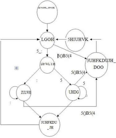
shown in Fig. 1.
Prior to normal operation, DDR SDRAMs must be powered up and initialized in a predefined manner.
When initial sequence completed, the design is
calibrated to ensure that correct data is captured in the ISERDES primitives. When initialization and
calibration is done, the controller set the phy_init_done signal HIGH and the memory is IDLE, which is signaled to start normal operation of
the design. Now, the controller can start issuing user write and read commands to the memory.
Figure 1. Simplified state machine of DDR SDRAM controller
In the design of controller, timing control of reading
and writing operations is completed according to the
column locations accessed for a given READ or WRITE command , and the value can be programmable to either
2, 4, or 8. In this design, the burst length is set to be 8 to guarantee the efficiency of read and write.
An AUTO REFRESH command is issued to the DDR memory at specified intervals of time to refresh
the charge to retain the data. If the memory is reading or
writing when issuing an AUTO REFRESH command, the controller will wait until the current operation
complete and then send a new command. If the user has read/write request during the refresh process, the
controller will not respond to the requests until the
completion of the current refresh cycle[6].
3. DESIGN OF DDR SDRAM CONTROLLER AND ITS READ AND WRITE STRATEGY OF
USER INTERFACE
The industry-standard DDR SDRAM memory has complex and rigorous control logic and timing
requirements, and the DDR SDRAM controller provides a
relatively simple user interface. It transforms all operations
to the DDR SDRAM memory into operations to user-end interface protocol. In order to shorten the design cycle, this
paper uses the Xilinx ISE 13.1 IP cores to implement the
DDR SDRAM controller.
In this design, DDR SDRAM is mainly used to
implement the storage of partial correlation results in the time domain dimension in acquisition algorithm of satellite navigation. Supposing the partial correlation
results are 4000*4096 matrix of n groups and the data
E-ISSN: 2321-9637
92
The partial correlation results after bit reshaping are
4000*1024 matrix of n groups, as shown in Fig. 2, and
are written into the DDR SDRAM in the sequence of
t(k) (k=1,2,3,...). The data are written in rows, and one
group of the data is written into one bank, which
occupies 4000 rows and 1024 columns. When read, it is
better to read in columns because of the FFT
computation in the frequency domain, so the traditional
method of reading in rows cannot be taken. But
changing rows in DDR SDRAM means a
PRECHARGE command to close the current row and
then an ACTIVE command to open the row for a
subsequent access. After completing these, the address
is accessible for the READ or WRITE command. Then
the read access delay for one data is (tRP + tRCD +
CL), which significantly reduces the efficiency of
reading and writing. Therefore, it is considered to read
several columns and then change to the next row. In
this design, 64 columns are read each time in a row. If
changing row needs 8 clocks, the read and write
In this design, we get 1024 partial correlation results to be stored every 2048 clocks. If we use traditional ways of reading and writing, that is, to read out the data of a BANK
which is continuously written in previously, it would require a large amount of on-chip RAMs to save them for FFT computation and make the time pressing for the
following data processing. In addition, it only takes 512 clocks to write the 1024 data to DDR SDRAM (without considering the refresh time), so the remaining 1536 clocks
become the unavailable dead time, which reduces the speed of data processing. Given this, this paper adopts the method of reading and writing alternatively, similar to the
ping-pong storage strategy in FPGA implementation[7]. After writing 1024 data to the DDR SDRAM, we read 16*64 data in the last BANK each time, which takes about
[(64/2)+8]*16 = 640 clocks. Using this method, we realize the seamlessly reading and writing. In addition, the user data FIFO will not overflow because of the total time for
reading and writing being less than 2048 clocks, and no read and write conflicts will happen on account of the same time taking for reading and writing each BANK.
In summary, the steps of the new strategy can be
described as follows:
step 1: Write the first group of partial correlation results after bit reshaping to the DDR SDRAM in rows(4000 rows in total).Now the BANK address is 0;
step 2: Set the BANK address to 1,then write in
the first row of the second group;
step 3: Set the BANK address to 0,then read out
16*64 data of the first group;
step 4: Repeat step2 and step 3 until finishing
writing the second group of data;
step 5: Deduce the rest by analogy to complete
reading and writing process of n groups.
4. FPGA IMPLEMENTATION OF DDR SDRAM CONTROLLER
This system uses Xilinx's Virtex_5 FPGA and
MICRON MT46V32M16XX-5B DDR SDRAM. The
density of the memory chip is 512Mb and the Data
Width is 16 bits. We need 6 memory chips in this design
E-ISSN: 2321-9637
93
MIG 3.6 (Memory Interface Generator) in Xilinx ISE 13.1 CORE Generator design tool can generate
DDR SDRAM controller based on V5 FPGA. The
implementation of DDR SDRAM controller contains four modules: the controller module, the user interface
module, the infrastructure module and the delay calibration module[8]. The logic block diagram is
shown in Fig. 3.
Figure 3. Logic block diagram of DDR SDRAM controller Implementation
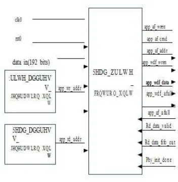
A.DDR SDRAM Controller User Interface Module
The user interface module generates the interface to let the user access to the DDR SDRAM through data buses, address buses and control signals. Fig. 4 shows the logic block diagram of this module.
In Figure 4, the write address generation unit and the read address generation unit generate the write data address app_wr_addr and read data address app_rd_addr respectively and send them to the read/write control unit. The read/write control unit is controlled by a state machine. According to the strategy described in 2.2, coupled with three status signals (wdf_almost_full, af_almost_full and phy_Init_done) getting from the DDR SDRAM, the control unit generates enable signals, address signals and status signals, such as app_af_wren, app_wdf_wren, app_af_addr, etc.
Figure 4. Logic block diagram of user interface module
B.DDR SDRAM Controller Module
The controller module initialize the DDR memory, parse the issued commands from the user, and generates all
the control signals required for the memory and the user interface. This module is mainly designed by MIG.
C. INFRASTRUCTURE MODULE
The infrastructure module generates the FPGA clock and reset signals. In this design, we use differential clocking (sys_clk_p and sys_clk_n). Differential clocks
are passed through global clock buffers before connecting to a PLL, and the output of the
sys_clk_p/sys_clk_n buffer is single-ended and is provided to the PLL input. The PLL unit generates
phase-shifted clocks like clk0 and clk90. In addition, the calibration clock(clk200) and all the reset signals are
generated in this module.
D. Delay Calibration Module
This module instantiates the IDELAYCTRL primitive
of the Virtex-5 FPGA. The IDELAYCTRL primitive is used to continuously calibrate the individual delay
E-ISSN: 2321-9637
94
5. FUNCTIONAL SIMULATION AND HARDWARE DEBUGGING
A. Functional Simulation and Analysis
This paper conducts functional simulation to the
aforementioned algorithm in ModelSim 10.1 to ensure
the correctness of the logic function and timing control. Fig. 5 and Fig. 6 show the simulation waveforms of
writing and reading respectively. Fig.7 shows the waveform of reading and writing alternatively. The
simulation results indicate that both the DDR SDRAM
and its control logic work properly.
Figure 5. Simulation waveform of writing data to the DDR SDRAM
Figure 6. Simulation waveform of reading data from the
DDR SDRAM
Figure 7. Simulation waveform of reading and writing alternatively
B. Hardware Debugging
The Chipscope analyzer is an integrated logic analysis
software of ISE, and we can observe the internal signal waveforms of FPGA logic design through it. With the
logic design and functional simulation completed, we add the CDC file to the project ,which includes the
signals to be observed and some trigger signals. Upon implementing this design, a BIT file is generated that
can be programmed using the ChipScope analyzer, then we can do real-time acquisition to the signals added in CDC file.
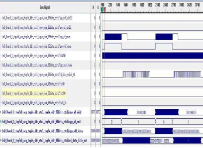
Waveform of reading and writing alternatively acquired by CDC is shown in Fig. 8. Hardware debugging
verifies that all the 6 memory chips can work in normal under the differential clocking and the designed
controller can write and read data correctly. Thus we realize the high-speed reading and writing of the partial correlation results between FPGA and the off-chip
E-ISSN: 2321-9637
95
Figure 8. Waveform of reading and writing alternatively acquired by CDC
6. CONCLUSION
Because of the complex and rigorous control logic and
timing requirements of DDR SDRAM, it requires very detailed work for correct implementation. Based on an
in-depth understanding of the basic principles of DDR SDRAM and algorithms of satellite navigation system, this
paper presents a new strategy for reading and writing and then implements the DDR SDRAM controller based on
FPGA. Compared to the traditional methods, the new strategy can realize the seamlessly reading and writing and
improve the efficiency of data processing in navigation
system. Functional simulation and hardware debugging prove the feasibility of the design.
REFERENCES
[1] Kaplan E D, "Understanding GPS Principles and Applications[M]". Boston, ArtechHouse , Inc,1996.
[2] Li Xi̅liang, Chang Qing and Zhang Qi-shan, DDR Controller Realized with FPGA in Satellite Navigation Receiver [J]. Radio Engineering of China, 2008, 38(2), pp. 51–54.
[3] Huang Yin, "Design and application of high-speed data storage system[D]",Huazhong University of Science and Technology,2009. [4] Micron Technology, Inc. Micron DDR SDRAM
512Mb DDR x4 x8 x16 Features. 2006.
[5] Picatoste-Olloqui E., Cardells-Tormo F. and Sempere-Agullo J., et al, Implementinghigh-speed double-data rate (DDR) SDRAM controllers on FPGA[C]. Berlin,Germany: Springer-Verlag, 2004..
[6] Ma ling, Yang Jun-feng, Song ke-zhu and Wang Yan-fang, A design of multiple DDR SDRAM controllers based on FPGA in a seismic data acquisition system[J]. Jounal of university of science and technology of China, 2010, 40(9), pp. 939–945.
[7] Wang Zhi, Luo Xin-min, Design and implementation of asynchronous FIFO based on ping-pong operation[J], Electronic engineer, 2005, 31(6),pp.13–16.