ABSTRACT
SU, HSUAN-JUNG. Continuous-Time Fractionally Spaced Equalization and Its Application in Capacitively Coupled Chip-To-Chip Interconnect. (Under the direction of Prof. Paul D. Franzon.)
There is an expanding gap between required bandwidth and achieved bandwidth due to
the scaling mismatch between IC technology and the rest of the electronic systems. There are
difficulties to increase the number of high-speed I/Os due to physical (material) reasons as
well as the constraint of overall power consumption. The power efficiency, thus, has become
the new metric for a high-speed I/O system.
Traditionally, AC coupled interconnect (ACCI) relies on the coupling capacitors as
passive equalizer to mitigate the frequency-dependent attenuation of the channel while
achieving superior power efficiency. However, the lack of flexibility of ACCI makes it less
capable of compensating for various range of channel and more susceptible to variation.
This work introduces the Continuous-Time Fractionally Spaced Equalization (CT-FSE), a
within-bit (high bandwidth) active equalization scheme, to complement the passive equalizer
induced pulse signaling by ACCI. According to the equations derived, two major
observations are presented, along with simulation result from a set of Matlab routines. The
CT-FSE structure supports bandwidth and power superior to a conventional feed-forward
equalizer (FFE) due to the lack of flip-flops and high-speed clock distribution.
The current-mode summation utilized in FFE has disadvantages in power consumption
and linearity and thus becomes less attractive when high-speed low-power equalization is
and increased reliability. A set of equations are derived to estimate the useable value of the
MultiCap, of which the range is bounded by I/O pitch, receiver sensitivity, and other
parameters. The parasitics of this device are proven to be negligible. The transceiver
achieved a speed of 5Gb/s with power efficiency comparable to state-of-the-art designs using
90nm technology nodes and beyond.
This work also introduces a buried capacitor (Embedded Cap) for signaling to improve
cost, reliability and parasitic inductance. The smaller nominal capacitance value can be
compensated by using a CT-FSE receiver equalizer. Tradeoffs in capacitance choice are
explained in detail. A nominal capacitance of around 1 pF provides a good choice for the
© Copyright 2012 by Hsuan-Jung Su
Continuous-Time Fractionally Spaced Equalization and Its Application in Capacitively Coupled Chip-To-Chip Interconnect
by Hsuan-Jung Su
A dissertation submitted to the Graduate Faculty of North Carolina State University
in partial fulfillment of the requirements for the Degree of
Doctor of Philosophy
Electrical Engineering
Raleigh, North Carolina
2012
APPROVED BY:
_______________________________ ______________________________
Dr. Paul D. Franzon Dr. John M. Wilson
DEDICATION
In loving memory of my parents,
BIOGRAPHY
Hsuan-Jung Su (Bruce) was born in Taitung, Taiwan in 1979. He received B.S. degree in
Electrical Engineering from National Tsing Hua University , HsinChu, Taiwan in 2001, then
he joined the Army of Taiwan until 2003. He received the M.S. degree and started Ph. D.
program in Electrical Engineering at North Carolina State University (NCSU) in 2006. And
he worked as a research assistant in NCSU until 2010. During the summer of 2006 and 2007,
he worked for IBM to develop de-embedding technique and Rambus to investigate noise
analysis methodology, respectively. He has been with Rambus since 2010. His interest
includes chip-to-chip communication, interconnect/package structures, and signal integrity
ACKNOWLEDGMENTS
I would like to thank my advisor, Dr. Paul Franzon, for all the encouragement and
inspiration. He always manages to give me very useful insights for matters inside and outside
of school. I would like to thank Dr. John Wilson for technical guidance and always keeping a
positive attitude toward my research, Dr. Joe Tracy for joining my committee without any
hesitation, Dr. Rhett Davis and Dr. Kevin Gard for giving me advices when I first started my
M.S. program and helping me make the decision to stay in NCSU for Ph. D. program, and
Elaine Hardin at Graduate School for all the help provided administratively.
I would like to thank Dr. Steve Lipa for helping me with research and experiments, Dr.
Jian Xu for the idea of embedded capacitor, Dr. John Wilson and Shep Pitts for suggesting
me the idea of MultiCap (separately). I enjoy working with Dr. Taeyun Kim, David Winick,
Dr. Julie Oh, Dr. Chanyoun Won, Dr. Hoon Seok Kim, Dr. Neil Di. Spigna, Dr. Thor
Thorolffson, Akalu Lentiro, and Dr. Ravi Jenkal. Also, I will never forget the nights and days
spent with Dr. Yongjin Choi and Evan Erickson in MRC429, especially before tapeout. I
would like to thank Pravin Patel and Trey Greer, my mentors during internship at IBM and
Rambus, respectively, my managers, Dr. Fred Heaton, Dr. John Eble, and Dr. Lei Luo for
motivating me at work and school, and all the colleagues at Rambus for constantly reminding
me to complete my degree.
I would like to thank my family and in-laws for giving all the heartwarming mental and
financial supports although living very far away (some on the other side of the planet), my
Last but not least, I sincerely thank my wife, Alice Yen-Fei Hsu, for always standing by
TABLE OF CONTENTS
LIST OF FIGURES ... ix
LIST OF TABLES ... xii
Chapter 1 Introduction ... 1
1.1 Motivations ... 3
1.1.1 Bandwidth Gap ... 3
1.1.2 Power Efficiency ... 5
1.1.3 Interconnect Structures ... 5
1.1.4 Equalization in Transceiver Design ... 7
1.1.5 Summary ... 10
1.2 Original Contribution ... 11
1.3 Dissertation Overview ... 13
Chapter 2 Background ... 14
2.1 AC Coupled Interconnect (ACCI) ... 14
2.1.1 Physical Structure ... 15
2.1.2 Schematic Models and Signaling and Method ... 17
2.2 Equalization Schemes ... 20
2.2.1 Passive Equalizations ... 21
2.2.2 Active Equalization ... 23
Chapter 3 Continuous-Time Fractionally-Spaced Equalization (CT-FSE) ... 28
3.1 Introduction ... 29
3.1.1 Transversal Equalization ... 29
3.1.2 Fractionally-Spaced Equalization (FSE) ... 30
3.2 Derivation of the CT-FSE Pair ... 32
3.4 CT-FSE Synthesizer in Matlab ... 41
3.4.1 Time-Domain Example (Pulse-Signaling) ... 43
3.4.2 Cross Frequency- and Time-Domain Example (NRZ Signaling) .... 45
Chapter 4 Transmitter-Side CT-FSE Utilizing MultiCap Voltage Summer ... 51
4.1 A Zero-Power Consumption MultiCap Structure ... 52
4.1.1 Parameter Analysis of the MultiCap Structure ... 54
4.1.2 Parasitic Capacitance of the MultiCap Structure ... 59
4.2 Voltage-Mode CT-FSE Transmitter Utilizing MultiCap Voltage Summer ... 62
4.3 Receiver Design ... 64
4.4 Design Flow ... 66
4.5 Measurement Results ... 66
Chapter 5 Receiver-Side CT-FSE with Embedded Capacitor ... 73
5.1 Embedded Capacitor and Channel Model ... 73
5.1.1 Analysis of Embedded Capacitor and Signaling Modes ... 76
5.1.2 Stub Length of the ACCI with Embedded Capacitor ... 81
5.2 Transmitter Design ... 82
5.3 Receiver Design ... 83
5.3.1 Current-Mode CT-FSE ... 84
5.3.2 High-Speed Latch ... 87
5.4 Design Flow ... 87
5.5 Simulation Results ... 89
Chapter 6 Conclusions and Future Works ... 93
6.1 Conclusions... 93
6.2 Future Works ... 96
REFERENCES ... 100
APPENDICES ... 105
Appendix A CT-FSE Synthesizer: Instructions and Matlab Programs (.m files) .. 106
A.1 Frequency-Domain Analysis then Synthesis: Sweep Filter Corner Freq. . 106
A.1.1 CT_FSE_Sweep_Filter.m ... 107
A.2 Frequency-Domain Analysis then Synthesis: Sweep Tdelay ... 110
A.2.1 CT_FSE_Sweep_Tdelay.m ... 111
A.3 Time-Domain Parameter Optimization (for Pulse Signaling) ... 114
A.3.1 Output files ... 117
A.3.2 CT_FSE_Optimizer_Pulse.m ... 118
A.3.3 smartlatch_new.m ... 125
A.4 Time-Domain Parameter Optimization (for NRZ Signaling) ... 128
A.4.1 Output files ... 129
A.4.2 GenerateChannelModel.m ... 130
A.4.3 CT_FSE_Optimizer_NRZ.m ... 135
A.4.4 smartlatch_NRZ.m ... 145
A.4.5 LFSR.m ... 148
A.4.6 Bit2Waveform.m ... 149
LIST OF FIGURES
Figure 1.1. CMOS scaling trends and bandwidth gap [5]. ... 4
Figure 1.2. Cross-section of a capacitive coupling interface with high-k under-fill [15]... 5
Figure 1.3. Top view of a high density ACCI [20]. ... 6
Figure 1.4. S21 plot of an ideal PCB microstrip with various lengths. ... 8
Figure 1.5. Comparing time-domain waveforms of two sets of channel input/output to demonstrate the effect of ISI ... 8
Figure 1.6. Block diagram of Feed-Forward Equalization. ... 10
Figure 1.7. Comparing various criteria between different equalization schemes and the expectation of this work. ... 11
Figure 2.1. Cross-section of a capacitive coupling interface with high-k under-fill [20].... 15
Figure 2.2. Schematic showing different configurations of CCI and LCI. ... 17
Figure 2.3. ACCI with small coupling capacitors generates pulse signal at RX input. ... 18
Figure 2.4. Equalization inserted into high-speed link to boost the high frequency signaling component. ... 20
Figure 2.5. Schematic of a R-C Filter. ... 21
Figure 2.6. Schematic of a T-Junction (RLC) Filter. ... 22
Figure 2.7. Schematic of (Left) R-L filter and (Right) R-TLine filter. ... 22
Figure 2.8. Schematic of a continuous-time linear equalizer (CTLE). ... 24
Figure 2.9. Block diagram of the FFE (or FIR) structure. ... 25
Figure 2.10. Block diagram of the Decision Feedback Equalization (DFE)structure. ... 26
Figure 2.11. Different ways of combining equalizers. ... 27
Figure 3.1. Block diagram of the conventional transversal filter structure. ... 29
Figure 3.2. Block diagram of the CT-FSE. ... 32
Figure 3.3. Similarity between the CT-FSE Pair and the Fourier Series in complex form. 35 Figure 3.4. The effects of k and τ on when linearly combining e-jωkτ in Eq. (3.7)... 35
Figure 3.5. Procedure of synthesizing HN(ω). ... 37
Figure 3.8. Different value of τ changes the available time point (indicated by arrows)
upon which equalization is applied. ... 40
Figure 3.9. The CT-FSE synthesizer implemented in Matlab. (Upper) Frequency-domain behavioral simulation. (Lower) Time-Frequency-domain parameter optimization. ... 42
Figure 3.10. CT-FSE synthesizer optimizes {ak} to achieve open eyes when τ varies. ... 44
Figure 3.11. Cross domain operation to verify the optimized k, ak, and τ are valid. ... 45
Figure 3.12. S21 of various channel lengths. ... 46
Figure 3.13. CT-FSE Inputs (Channel outputs) vs. CT-FSE Outputs (Time-Domain Optimizer outputs). ... 47
Figure 3.14. Target HI(ω) (=1/ S21) vs. Synthesized HN(ω) according to k, ak, and τ from Time-Domain Optimizer ... 48
Figure 3.15. System overall frequency response = S21 × HN(ω) ... 50
Figure 4.1. The cross-section showing MultiCap replace one pad in the ACCI structure. . 52
Figure 4.2. Schematic symbol of MultiCap and its usage as a voltage summer. ... 52
Figure 4.3. TX-side pre-emphasis realized by CT-FSE utilizing MultiCap voltage summer. ... 53
Figure 4.4. Top view of the MultiCap structure includes a matrix of silicon top metal plates and a shared big bottom plate on package. ... 55
Figure 4.5. The parasitic capacitances between a pair of CC and ground ... 59
Figure 4.6. Schematic model for the pair of CC shown in Figure 4.5 ... 60
Figure 4.7. Calculation results using (4.9) vs. Sonnet simulation result ... 61
Figure 4.8. All-digital complementary CT-FSE TX. ... 62
Figure 4.9. Detail of a slice of TX gain and driver stages. ... 63
Figure 4.10. The MultiCap structure implemented by on-chip VNCAP ... 63
Figure 4.11. Detail of high-speed latch RX ... 64
Figure 4.12. Block diagram of the design flow for CT-FSE TX utilizing MultiCap voltage summer ... 65
Figure 4.13. Die photo with TRX area and PCB photo with channel setup. ... 67
Figure 4.14. PCB cross section and the real measurement setup on probe station. ... 68
Figure 4.15. The overall test setup when displaying waveform on Oscilloscope. ... 69
Figure 4.18. RX output: recovered 5Gb/s NRZ bit-stream. ... 71
Figure 5.1. Structure of package cross-section, including embedded capacitors for both power supply decoupling and ACCI signaling. ... 74
Figure 5.2. Simplified schematic of the ACCI channel with embedded capacitor. ... 75
Figure 5.3. Simulated S21 plots of the channel shown in Figure 5.2. ... 76
Figure 5.4. The center frequency and bandwidth of the channel-equivalent BPF change as CC increases ... 77
Figure 5.5. The step response of the ACCI channel with various CC. (Bottom right) The way to calculate time for maximum run length. ... 79
Figure 5.6. Simulated S21 plots of the channels with various stub length. The difference in peak is around 2dB. ... 82
Figure 5.7. TX is made of a pair of complementary progressively-sized inverter chains. .. 83
Figure 5.8. RX block diagram. ... 83
Figure 5.9. Block diagram of the RX CT-FSE. ... 84
Figure 5.10. Matlab simulation results shows the open 5Gb/s eyediagrams of the CT-FSE with tap delay (τ) varies from 75ps to 225ps. ... 85
Figure 5.11. Detail of the building blocks in RX CT-FSE. ... 86
Figure 5.12. The common-mode feedback circuit utilizing Gilbert cell to maintain CT-FSE output common-mode voltage. ... 86
Figure 5.13. The high-speed latch is a non-clocked regenerative comparator with common-source pre-amplifier. ... 87
Figure 5.14. Design flow of the system (RX CT-FSE with embedded capacitor) ... 88
Figure 5.15. Time-domain waveforms of the delayed RX inputs. ... 89
Figure 5.16. Comparison of the waveforms before and after CT-FSE is turned ON. ... 89
Figure 5.17. The CT-FSE eliminate most ISI in RX input, and the latch recovers the signal back to 3.33Gb/s NRZ signals. ... 90
Figure 5.18. Detail current and total power consumption of each RX block. ... 91
Figure 6.1. Comparison of power efficiency (mW/Gb/s) and topology. ... 94
Figure 6.2. Block diagram of the CT-FSE with adjustable delay elementes. ... 96
Figure 6.3. Block diagram of the CT-FSE with non-uniform delay τk. ... 97
LIST OF TABLES
Table 3.1. Optimized tap weights, ak, and eye opening for 5 different channel length. ... 48
Table 4.1. Comparison of Performance. ... 72
Table 5.1. Investigation of available materials for embedded capacitor. ... 74
Table 5.2. Timing and Circuit Requirement for Various CC. ... 80
Chapter 1
Introduction
Since the invention of integrated circuit (IC) technology in the 1950’s, there have been
significant progresses in CMOS manufacturing, packaging, testing, material, and system
design. Observing from higher level, the progresses in the electronic components enable
rapidly improvement in high-performance electronic products, such as gaming platform,
portable devices, server, etc. In every new generation, these products are expected to have
exponential growth in performance.
One of the most critical factors for the exponential performance improvement is the
communication between electronic components. For instance, as much information as a
microprocessor can process in a short amount of time, or as much computing power as a
microprocessor can have, it still needs proper I/Os to exchange information with the outside
Unfortunately, the issues of I/O bandwidth can easily be solved were it not for the system
power limitation. Assume there is no issue for heat dissipation; for the gaming platform, the
system power limit is the maximum power rating for a household wall socket; for a portable
device, the time lapse between each battery recharge; and for the server, the total available
output in megawatt (MW) provided by a dedicated power plant. To overcome the
performance bottleneck in system I/Os while consuming as less power as possible, this
dissertation explores solutions to be applicable on majority of high-speed chip-to-chip
communication. The following chapters show some design considerations involved with
circuit and interconnect co-design, and the combination of different concept in each field
resulting in state-of-the-art power efficiency.
Due to the multidisciplinary nature of the chip-to-chip communication, the angle of
researches in this dissertation is twofold: interconnect structure and transceiver (TRX) design.
One cannot only optimize the interconnect structure while expecting the TRX to remain
unchanged. On the other hand, a different topology for TRX design would affect the
compatibility with the interconnect structure. That is, a successful chip-to-chip
communication requires the combination and tradeoff between good power efficiency for the
1.1
Motivations
1.1.1
Bandwidth Gap
In 1965, Moore predicted that the number of transistor counts in a single wafer would double every year [1] (that was more from the viewpoint of cost per component dropping exponentially). Later this so called “Moore’s Law” was altered for better accuracy to
“doubling transistor counts in a die for every two years” or “doubling performance per chip
every 18 months if the performance of the transistor itself is counted”. In fact, almost 30
years later, Moore himself compared the history in transistor counts per die against the
prediction to show the reality lagging mildly [2] Nonetheless, the Moore’s Law has governed
the development of the modern CMOS technology. The semiconductor foundries and the
International Technology Roadmap for Semiconductors (ITRS) [3] try to follow the
exponential performance growth described by Moore’s Law. For each newer generation, it is
expected that the chip performance would increase exponentially.
The number of interconnects per die, in contrast, has a different story. As predicted by
Rent in the 1960’s and described by Landman and Russo in 1971 [4], the number of pins
with regarding to the number of logic gates should also follow an exponential law, with the
exponent related to the level of complexity of the logic: Number of pins = K × Gatesr. As
green dots at the bottom shows the history of real bandwidth. It is clear that there is an
expanding gap between required bandwidth and achieved bandwidth.
Figure 1.1. CMOS scaling trends and bandwidth gap [5].
During the past decade, more and more literatures in high-speed chip-to-chip communication (or serial link)1 paid attention to this issue of bandwidth gap. For example, Kuroda and Miura in 2006 [6] addressed this issue and compared the existing trend with the
prediction by Rent’s rule (with slightly modified K and r). They also pointed out the gap
between real annual bandwidth growth and required annual growth of is 28% vs. 45%. Also
for example, Palermo et al [7] in 2008 mentioned ITRS predicted that that trend of aggregate
I/O bandwidth (per pin data rate × I/O number) was required to grow exponentially.
1 Throughout this dissertation, “high-speed chip-to-chip communication” and “serial link” are used
Gates x GHz
Doubles every 16 months
Signal Pins x GHz
Doubles every 28 months
Year º º º º º º º º º º º º º º º º º º º º
1976 1980 1984 1988 1992 1996 2000 2004 2008
10-1 10 101 102 103 104 105 106 107 108 109 1010 8086 286 386 486 P1 P2 P3 P4(180n) dual Xeon P4(90n)
Pins x GHz from Rent’s Rule
1.1.2
Power Efficiency
The newer update of ITRS in 2009 [3] maintains the same point of view on the increasing
I/O bandwidth gap while stating the difficulties to increase the number of high-speed I/Os
due to the constraint of overall power consumption. It also mentioned the recent trend of
integrating memory controller inside microprocessors further exacerbate the bandwidth gap
since the memory interface is going to have higher and higher bandwidth requirement
(DDR4 is predicted to hit 4Gbps [9]). Therefore, we know that the real bottleneck in
chip-to-chip communication, instead of just the I/O bandwidth, is the I/O bandwidth per Watt.
Poulton et al [8] presented one of the first serial link designs that targeted at better power
efficiency (mW/Gb/s) instead of pure high bandwidth. In terms of power efficiency, they
achieved performance an order of magnitude better than the rest of the high-speed serial link
designs. To satisfy the requirement of better power efficiency, a serial link design needs not
only support high bandwidth but also consume least amount of power possible.
Figure 1.2 shows the cross-section of a capacitively coupled interconnect (CCI) structure
with high-k dielectric underfill. Luo et al. [21] demonstrated the possibility to apply CCI with
PCB channels up to 45cm, besides enabling high per-pin data rate.
Figure 1.3. Top view of a high density ACCI [20].
As shown in Figure 1.3, Wilson et al. [20] presented the possible setup for ACCI to
support high-density high-speed I/O at the peripheral of the die, low inductance
power/ground distribution via the centrally located DC buried bumps, and the underfill inlet
from the corners of the die. The high-k underfill material was developed by Kim et al. [50] to
reduce the area requirement for the capacitor arrays, relax the constraints on the dielectric,
and provide stress relief between die and substrate. This leads to potential improvement in
yield, and the increase in long-term reliability. Therefore, ACCI not only supports high
aggregate bandwidth by enabling high-density I/O structure and high per-pin data rate, but it
also shows some physical advantages over other interconnect structures.
As noted by Luo et al. [19], the main difference between ACCI and traditional capacitive
Centrally located DC bumps
Peripheral AC I/O Area on die above
1000 times of those in ACCI. The series capacitors in ACCI are small because they function
as passive equalizers. When pushed toward highest bandwidth possible, as described in detail
later in section 2.1.2, the series capacitance could become so small that the RX input signal
amplitude drops below the receiver (RX) sensitivity threshold. Therefore, the only solution to
this shortcoming is to devise a new I/O structure that inherit all the advantages of ACCI and
supports a novel active equalization scheme to complement ACCI.
1.1.4
Equalization in Transceiver Design
The main challenge for a transceiver (TRX) to support high data rate is the ability to
compensate for the frequency-dependent attenuation of the channel. A typical PCB channel
has a low-pass response due to the skin effect (∝ f1/2) and dielectric loss (∝ f) [10]. As Dally and Poulton pointed out in [37], the frequency-dependent attenuation causes inter-symbol
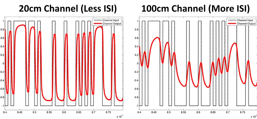
interference (ISI). Take the microstrip channel shown in Figure 1.4 for example, with
Nyquist frequency of 5GHz, the S21 plot shows the attenuation difference between DC and
5GHz could increase from 3.3dB for a 20cm microstrip line to 16.6dB for a 100cm one. For
backplane applications, such as the tens of inches backplane channel in [13], the loss for
6Gb/s bit stream (Nyquist rate of 3GHz) could range from 20dB to over 30dB. The
time-domain plot in Figure 1.5 compares the inputs/outputs between a short channel with less
high-frequency attenuation (left) and a long channel with more high-frequency attenuation
frequency loss, the presence of process-voltage-temperature (PVT) variation could also
significantly affect the TRX performance.
Figure 1.4. S21 plot of an ideal PCB microstrip with various lengths.
0
-20
-60
10
610
710
810
910
1010
115GHz
-40
Freq. (Hz)
S
21(dB
)
-3.3dB
-16.6dB
Ideal PCB Microstrip (Simulation)
Vout
Vin
To mitigate the problem of frequency-dependent attenuation (or ISI) and PVT variation,
the TRX requires equalizations to add flexibility to the system. There are two categories of
equalization: 1.) passive equalization utilizing passive components as filters, and 2.) active
equalization consisting of active circuitry to synthesize the filter response.
Passive equalization schemes, benefiting from simple circuits, enable high-speed serial
link with low power consumption. Luo et al. [19] and Wilson et al. [20] demonstrated that
AC Coupled Interconnect (ACCI) has one of the best power efficiency (1.97mW/Gb/s)
among various passive equalization schemes. However, there are two major problems
associated with passive equalization schemes: flexibility and limited channel length. The
passive equalizer in ACCI – capacitors, for example, are formed between silicon and package;
thus, the capacitors are fixed during manufacturing process, after which there is no
adjustability on the capacitor value, hence the fixed amount of equalization. Further, passive
equalization can only support PCB channel up to certain length (about 30cm for ACCI [21]).
Although the use of a smaller capacitor can shift the filter peak toward higher frequency and
compensate more high-frequency attenuation from longer channel, it also decreases the
signal swing. Therefore, there is a limit beyond which the signal magnitude will be
attenuated below the noise floor of the system; i.e., the system is swing limited.
Active equalization utilizes the transistor (amplifier) characteristic or the digital filtering
technique to improve the flexibility of the TRX, compensate for the frequency dependent loss,
and extend the upper limit of the channel length. The most commonly used active
(FFE, Figure 1.6), such as those used in [24] and [25]. The FFE structure is a good
compromise between complexity, power consumption, and equalization performance.
Although the FFE structure is straightforward and flexible, unfortunately, this scheme
usually dissipates a significant amount of power due to the use of 1.) current summation
block (combined with transmit driver), 2.) high-speed flip-flops, and 3.) high-frequency
clock distribution network. Therefore, a novel active equalization scheme is required to keep
the flexibility of the TRX while eliminating these three issues to save power consumption.
Unit
Delay
Σ
x
a
0Unit
Delay
x
a
1Unit
Delay
x
a
2Σ
Unit
Delay
x
a
3Σ
x[n] x[n-1] x[n-2] x[n-3]
y[n]
Figure 1.6. Block diagram of Feed-Forward Equalization.
1.1.5
Summary
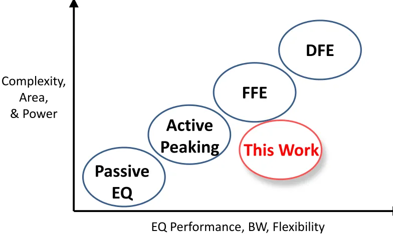
In order to close the gap between required aggregate bandwidth and achieved bandwidth
while supporting low power operation, we need innovation in equalization scheme as well as
interconnect structure. The overall system should be able to integrate interconnect and
better than a traditional FFE and power efficiency close to passive equalization. Notice the
detail of each equalization scheme is described in section 2.2.
Figure 1.7. Comparing various criteria between different equalization schemes and the expectation of this work.
1.2
Original Contribution
The research in this dissertation achieves further improvement in the power efficiency
and extends the capability of the passive equalization in ACCI by complementing it with a
within-bit high-bandwidth active equalization. The intention of the dissertation is to
demonstrate a consistent methodology for system design, by deducing analytical equations
for the fundamental design parameters first, and then build components on top of the
EQ Performance, BW, Flexibility
Complexity,
Area,
& Power
DFE
FFE
Active
Peaking
Passive
EQ
1. The CT-FSE theory to mathematically explain why and how feed-forward equalization
(FFE) with continuous-time delay would operate. Chapter 3 presents the derivation of the
equations that describes the CT-FSE theory. The equations can be generally applied to a
FFE with any continuous-time delay, in addition to the conventional unit-delay case.
Appendix A shows a group of Malab programs developed to verify the theory.
Integrating CT-FSE structure into high-speed transceiver design would eliminate the use
of high-speed clock distribution and save power.
2. A novel multi-capacitor (MultiCap) structure to enable zero power consumption in
voltage summation for voltage-mode CT-FSE (or any FFE) in transmitter (TX). Chapter
4 analyzes the MultiCap structure and provides equations for searching the usable range
of dimension and material parameters. The combination of MultiCap and voltage-mode
CT-FSE solves several problems of conventional current-mode FFE structure and results
in power efficiency comparable to TX designs implemented in more advanced CMOS
process nodes.
3. A method to combine the passive equalization realized by the embedded capacitor in
printed circuit board (PCB) and the active equalization realized by current-mode CT-FSE
at the RX end. The capacitor embedded in PCB has potential to improve cost, reliability
and parasitic inductance. Chapter 5 implements current-mode CT-FSE compatible with
ACCI pulse signaling, analyzes the embedded capacitor structure for usable value, and
investigates the material of embedded capacitor to ensure compatibility with developing
1.3
Dissertation Overview
Chapter 2 reviews the backgrounds of two topics separately, including ACCI and
equalization schemes implemented in high-speed link design. Since both topics are very
broad in nature, this dissertation only covers the qualitative introduction and comparison with
proper references. Chapter 3 derives the theory of CT-FSE in equations and proves the
analysis with Matlab programs (source codes in Appendix A). Chapter 4 presents a novel
Multi-Capacitor (MultiCap) structure to be utilized as the voltage summation block when
combined with TX-side CT-FSE. Chapter 5 demonstrates the idea of incorporating active
equalization (CT-FSE) with passive equalization (PCB-embedded capacitor). Both Chapter 4
and Chapter 5 have design flow sections dedicated to show how the overall system is put
together, including navigating through different domains of the multi-disciplinary work.
Chapter 2
Background
2.1
AC Coupled Interconnect (ACCI)
ACCI was introduced in the early 1990’s to address the problem of limited space and
aggregate bandwidth for I/Os on a multichip module (MCM) [14]. In early 2000’s, Mick et al.
[17] demonstrated the feasibility of using buried bump in flip-chip configuration to realize
ACCI. The possibility of high density interconnect with high structural reliability were
presented later by Wilson et al. [20]. And the power efficient transceiver design is also by
Luo et al. [19]. Therefore, this technology is also well known for its versatility in connector
designs and superior power efficiency.
There are two aspects of ACCI (or CCI) that makes it more attractive than conventional
chip-to-chip channel:
Physical Structure
2.1.1
Physical Structure
The fundamental concept of ACCI is to replace the DC connections (that transfer AC
signals) of typical chip I/Os and inserts non-contacting passive components in series with the
chip-to-chip channel. Since there is no hard requirement on where and how those connections
should be replaced, there are a variety of structures that utilize the concept of ACCI. A more
complete description regarding the ACCI technology in more detail can be found in the
dissertation by Xu [15], but in general ACCI can be broken down into two major categories:
Figure 2.1. Cross-section of a capacitive coupling interface with high-k under-fill [20].
Capacitively-Coupled Interconnect (CCI): As presented by Mick et al. [18],
coupling capacitors are created between die and substrate top metal in a flip-chip
environment. As shown in Figure 2.1, one plate of the capacitor is the silicon top
metal, and the other plate of the capacitor is located on the substrate, which could
thermal-stress relief characteristic [50] to increase the long-term reliability. It is
found that CCI is capable of signaling at higher speed [19] due to less parasitic in
the interconnect structure as well as low power due to the nature benefit of
voltage-mode signaling.
Inductively-Coupled Interconnect (LCI): This configuration is similar to CCI with
the capacitors replaced with coupled coil (inductors). Between the two inductors,
the signal is transferred through the magnetic field (or current). Xu [15] found that
LCI is capable of transfer signal through larger gaps (tens of µm as opposed to
single digit of µm in CCI) due to the penetrating magnetic field as well. LCI also
tends to consume more power due to the nature of the current-mode signaling. For
more detail related to LCI, the dissertation by Chandrasekar [16] can be referred
Depending on the scenario in which the interconnect structure is implemented in, there
are other applications for CCI and LCI. For instance, there have been examples of ACCI
utilized in 3-dimensional integrated circuit (3DIC) as presented by Davis et al. [31]. Also,
there are advanced variations for CCI and LCI in connectors, including daughtercard
connectors proposed by Chandrasekar [16] and sockets proposed by Xu [15]. This
2.1.2
Schematic Models and Signaling and Method
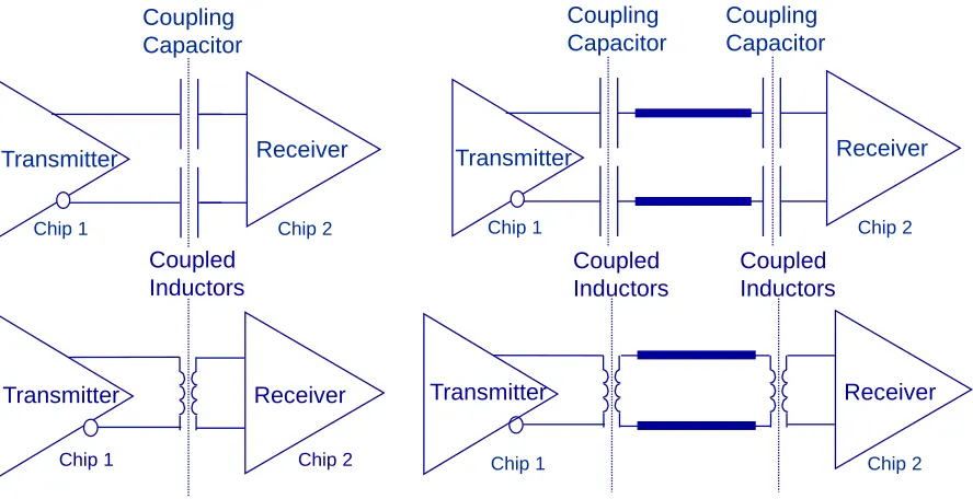
Figure 2.2. Schematic showing different configurations of CCI and LCI.
Several generalized schematic models for the ACCI system are shown in Figure 2.2,
including one capacitor without channel, two capacitors on two side of the channel, one pair
of inductors without channel, and two pairs of inductors on two side of the channel. The
requirements for signaling imply different designs of TRX circuitry and different ways of
connecting to ACCI; i.e., voltage-mode signaling for CCI and current-mode signaling for
LCI. As long as the signal integrity analysis satisfies the design budget, it is the choices of
designers to determine either single-ended or differential signaling is more suitable for the
specific application.
Chip 1 Chip 2
Coupling Capacitor
Coupling Capacitor
Transmitter Receiver
Transmitter Receiver
Coupled Inductors
Coupled Inductors
Chip 1 Chip 2
Transmitter Receiver
Chip 1 Chip 2
Coupled Inductors
Chip 1 Chip 2
Coupling Capacitor
Figure 2.3. ACCI with small coupling capacitors generates pulse signal at RX input.
A most significant difference between ACCI and other type of interconnect, besides the
structure, is the signaling mode. The passive components of small value in series with the
channel in ACCI normally induce pulse signaling. The effect is illustrated very well by
Salzman et al. [14] and Luo et al [19], and we redraw the concept in Figure 2.3. The voltage
coupled across the capacitors would be differentiated, leaving only the edge information as
pulses at the RX input. As opposed to NRZ (non-return-to-zero) signaling, the pulse
signaling have zero DC component (due to AC coupled) and have positive pulse when there
is a low-to-high transition at TX output and negative pulse when there is a high-to-low
transition. This time-domain behavior implies that the data is carried by the edge information.
Therefore, the data rate can be pushed higher if each edge is narrower (or the narrower
pulses). It also verifies the effect of passive equalization in ACCI (further detail in section
2.2.1).
The only way to make pulses narrower in ACCI is to decrease the size of series
capacitors or inductors, which also has a side effect of decreasing the pulse amplitude. This
i ii iii
RX TX
i
ii
iii
1.8V
60mV
technologies that uses off-chip passive components to perform equalization: the lack of
flexibility (or less degree of freedom).
As Luo et al. presented in [19], the high-passing coupling capacitors need to matches to
the channel for extreme performance. When pushed toward highest bandwidth possible, the
more attenuation of the channel, the smaller the series capacitance or inductance need to be.
In other words, the appropriate value of the AC components depends on the channel
attenuation. To compensate for a very long channel with large amount of
frequency-dependent attenuation, the ACCI system would require series capacitance or inductance so
small that the signal amplitude goes below the RX sensitivity threshold. In other words, it is
possible to have a perfect open eyediagram at the RX input, but the RX latch is not sensitive
enough to recover the pulse signal.
To add the flexibility (or more degrees of freedom) to the ACCI technology, proper
equalization scheme needs to be adopted. The nature of the pulse signaling in ACCI leaves
only edge information at the RX input. Thus, it is more suitable to have the equalization
operating within one bit period. After a short introduction to general equalization schemes in
section 2.2, this dissertation presents a novel CT-FSE scheme in Chapter 3 to be combined
2.2
Equalization Schemes
Figure 2.4. Equalization inserted into high-speed link to boost the high frequency signaling component.
The bandwidth bottleneck for a high-speed chip-to-chip link is usually the channel. As
described in section 1.1.4, the frequency-dependent attenuation of the channel causes ISI and
high-speed serial links requires equalizations of some sort. The upper half of Figure 2.4
indicates the two possible locations to insert the equalization block: TX-side or RX-side..
The frequency domain plot at the lower half of Figure 2.4 shows that high-speed link utilizes
pre-emphasis and/or de-emphasis to obtain an equalized channel with flat response within
Nyquist frequency. Equalization in general is able to add flexibility to a chip-to-chip
Frequency
Channel
Bit-rate/2
Frequency
EQ
Bit-rate/2
Frequency
Equalized Channel
Bit-rate/2
RX
EQ
chapter separates equalization schemes into two categories: passive equalization and active
equalization.
2.2.1
Passive Equalizations
Passive equalization achieves filtering function by utilizing passive components, such as
capacitors, inductors, transmission line, or any combination of them.
Figure 2.5. Schematic of a R-C Filter.
R-C filter: As shown in Figure 2.5, it consists of a resistor in parallel with a capacitor. It
is the most basic implementation for passive equalization. Shin et al [32] demonstrated an
on-package discrete implementation of the R-C filter and it supported data rate up to 10Gbps.
Although ACCI is a special case of this filter (R = ∞), R-C filter cannot be integrated with
CCI since it is less likely to manufacture the resistor between silicon die and substrate as a
typical CCI structure.
R
Figure 2.6. Schematic of a T-Junction (RLC) Filter.
T-Junction (R-L-C): As shown in Figure 2.6, Sun et al [33] presented a “T” configuration
that consists of resistors, inductors, and capacitors to form a high-pass filter (HPF). The
differential version of this filter supported data rate up to 20Gbps.
Figure 2.7. Schematic of (Left) R-L filter and (Right) R-TLine filter.
R-L Termination: As shown in Figure 2.7, Guo et al [34] presented a method to insert an
inductor on the RX termination to deliberately cause mismatch and thus achieve equalization.
In the same literature they also presented a variation that replaces the inductor with a section
of high-impedance transmission. It is demonstrated to support data rate of 5Gbps.
R
C
R
R
L
L
R
R
ACCI (Coupled-C/L): As shown in Figure 2.2, ACCI use series capacitors (or
transformers) as signal filter. More detail is already described in section 2.2.1. Note the major
difference between ACCI and other passive equalization scheme are the small value of the
passive component and the loss of DC information due to lack of DC path. The former
generates pulse signaling and the later implies a requirement of signaling bias generation
built into the RX circuitry.
All passive equalization schemes have one shortcoming in common: the lack of
flexibility. To complement the passive equalization that already performed de-emphasis on
the low frequency component, an active equalization only needs to boost the really high
frequency component. This relaxes the sharpness requirement of the filter, but the bandwidth
requirement of the filter is still as high as the case without passive equalization. Take the
pulse signaling in ACCI for example, at RX input, most of the frequency-dependent
attenuation induced ISI is mitigated, leaving only minor “tail” that is mostly within one bit
period for the active equalization to deal with. Therefore, the bandwidth requirement for
active equalization in ACCI is even higher without the effect of the coupling capacitors.
2.2.2
Active Equalization
Although passive equalization is simple and does not consume power, sometimes, a
high-speed serial link needs to sacrifice in system complexity and power consumption for better
active equalization that handles within-bit ISI (later in Chapter 3, the equations proves the
within-bit capability is equivalent to high-bandwidth). There are many different topologies of
active equalizations, among which, some utilizes the knowledge in analog/RF circuit design,
and others adapt the digital filter structure from digital signal processing (DSP).
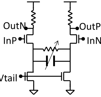
Figure 2.8. Schematic of a continuous-time linear equalizer (CTLE).
As shown in Figure 2.8, continuous-time linear equalization (CTLE), or sometime simply
linear equalizer (LE), is a capacitive source-degenerated differential amplifier. At low
frequency, the two tail current work independently and the gain is low. At high frequency,
the capacitor acts as a short and the structure work as a differential amplifier work boost the
gain. The tunability can be achieved by adjusting the value of the resistor and/or capacitor.
This circuit can be fairly efficient since it was used by Palmer et al. [51], one of the most
power efficient serial link designs. Lee [22] presented equations to describe the transfer
function of LE. He also proposed an improved version with inductor load that supports
20Gbps data rate.
Vtail
InP
InN
Unit Delay
Σ
x
a
0Unit Delay
x
a
1Unit Delay
x
a
2Σ
Unit Delay
x
a
3Σ
x[n] x[n-1] x[n-2] x[n-3]
y[n]
Figure 2.9. Block diagram of the FFE (or FIR) structure.
In the domain of digital signal processing, the finite-impulse response (FIR) is one of the
most well-known filters. As shown in Figure 2.9, the x[n] and y[n] are the input and output
signals, respectively. And a0 to a3 represent the tap weights. The output, y[n], is a weighted
sum of all the delayed version of input, x[n]. The unit delay is normally implemented with
clocked flip-flop. Dally and Poulton [37] integrated the FIR algorithm into a current-mode
transmitter and allow for pre-emphasis right on the high-speed driver node. This topology is
very straightforward and linear. I.e., it will boost/equalize signal, ISI, and noise. This
topology is at least as useful as LE since they both have more linear and predictable default
filter response (some adaptive algorithm requires a default setting that works without
calibration). FFE is more flexible and potentially higher bandwidth than LE when it has more
taps (generally more than 2 taps). Therefore, it can be seen in many literatures that involves
with more practical researches, such as [24] and [25]. However, FFE consumes a lot of
Figure 2.10. Block diagram of the Decision Feedback Equalization (DFE)structure.
The DFE, shown in Figure 2.10, has the reverse mechanism as FFE. As described by
Belfiore and Park [12], assume the output of the summation block is the original signal
without any ISI; the tap-delay-weighted chain should emulate the negated channel response
and feedback this information (which is actually the residue of the ISI added onto the
following bits) to the summer. Therefore, when the following bit arrive at RX input, the ISI
on x(t) can be subtracted out at the summer state. This topology is nonlinear – it will not
boost the noise added to x(t) because the comparator and the flip-flop (which are nonlinear
themselves) saturate the signal all the way to supply rail voltage level. However, the DFE
structure consumes even more power than FFE due to tap-delay-weighted chain (just like
FFE), besides the auxiliary circuitry to support the DFE operation. In addition, DFE has a
known issue of error propagation. I.e., when an error occurs, the likelihood of making
another error on the next bit is increased drastically.
Unit
Delay
Delay
Unit
Delay
Unit
Σ
x(t) y(t)
x
a
1x
a
2Figure 2.11. Different ways of combining equalizers.
In addition to all the blocks being implemented individually, many literature combine
two or more equalization schemes together. As shown in Figure 2.11, multiple equalizers
(whether different or the same) can be combined in parallel, in series, or one integrated into
another as a building block. For example, two modified T-junction passive equalizer were
combined in parallel in [23]; Payne et al. [24] combined the FFE at TX and DFE at RX; and
Higashi et al. [25] in the RX utilized the split-path approach to combine signals from analog
equalizer blocks, which integrated LE as part of the RX pre-filter. The complexity of the
overall system is a direct result of trading-off between performance and power.
Equalizer2 Equalizer1
Σ
Equalizer1 Equalizer2 Parallel (Split-path)Serial (Cascade)
Chapter 3
Continuous-Time Fractionally-Spaced
Equalization (CT-FSE)
This chapter introduces the concept of utilizing continuous-time delay, instead of a unit
delay or fractional delay, in a conventional FIR structure. The novel equalization structure is
name Continuous-Time Fractionally-Spaced Equalization (CT-FSE). According to the
equations derived for the CT-FSE theory, two major observations are presented along with
select examples from a set of Matlab programs (more examples and source codes in
Appendix A). The CT-FSE has bandwidth and power superior to conventional FIR structure
3.1
Introduction
3.1.1
Transversal Equalization
Unit Delay
Σ
x a0
Unit Delay
x a1
Unit Delay
x a2
Σ
Unit Delay
x a3
Σ x[n] x[n-1] x[n-2] x[n-3]
y[n]
Figure 3.1. Block diagram of the conventional transversal filter structure.
One simplest way of realizing an active equalizer is the conventional transversal filter
structure, shown in Figure 3.1, which is also known as finite-impulse response (FIR) filter in
the DSP field, or feed-forward equalizer (FFE) if implemented in transceiver design. Given a
discrete delay of one bit period, the output, y[n], of the transversal filter is the weighted-sum
of the input, x[n]:
[ ] k [ ]
k
y n =
∑
a x n−k (3.1) , where ak is the tap weight. Perform Fourier Transform on both sides of (3.1) andobserve the equation, the filter transfer function is the discrete Fourier transform of the tap
𝐻(𝜔) =� 𝑎𝑘𝑒−𝑗𝜔𝑘 𝑘
(3.2)
Therefore, given a known filter response and follow the classic mathematics derivation
for Fourier series, the tap weights can be calculated as:
2
1
( ) 2
j k k
a H eω d
π
ω ω
π
∫
= (3.3)
The pair of (3.2) and (3.3) enables direct analysis and synthesis 2when designing a transversal filter. An early example of the high-speed link implementation of this structure
was presented in [37].
3.1.2
Fractionally-Spaced Equalization (FSE)
The concept of using a fractional tap delay (Figure 3.2) instead of unit symbol interval in
a transversal filter was first introduced in the 1970s. The mathematic theory, analysis, and the
fractionally spaced equalization (FSE) system implementation were realized in the sampling
domain, i.e., there are asynchronous sampling actions at the input, output, or the tap delay
line, due to the original intention of integrating FSE into digital adaptation hardware as
presented by Ungerboeck [27]. In the 1980s, Gitlin and Weinstein [26] demonstrated the
performance improvement of FSE over a conventional transversal equalization. Qureshi [28]
compared the conventional transversal equalization scheme and the FSE scheme, and
2
discussed the characteristics of FSE in detail, including behaviors of different adaptation
algorithms.
Recently, just as Dally and Poulton [37] brought the concept of FIR to TRX designs,
several literatures adopted the concept of continuous-time delay element to FSE designs.
These newer design uses continuous-time delay element, such as the current-mode biquad
[29], the inductively peaked inverter[30], the LC-delay lines in [35], and the combination of
LC-delay line and buffer in [36]. Although these designs could function based on the
experiment result, there was lack of direct mathematic proof on how and why the FSE
structure would work with continuous-time delay element not exactly at fractions of a period.
Therefore, most of these designs select a delay of half-unit interval (T/2) without knowing
that the FSE structure would also function properly as long as the delay is within a proper
range. Therefore, the rest of this chapter derives the equations of Continuous-Time
Fractionally-Spaced Equalization (CT-FSE), analyzes of the filter behavior in detail, gives
key observations, proposes method to do design tradeoffs, and provides Matlab programs for
3.2
Derivation of the CT-FSE Pair
Figure 3.2. Block diagram of the CT-FSE.
Figure 3.2 shows the block diagram of the CT-FSE structure. This structure uses the
continuous-time tap delay, τ, which can be any analog delay besides unit delay. In
continuous-time domain, the output, y(t), can be written as the linear combination of the
input, x(t), of which each delayed version is scaled by corresponding tap weights:
( ) k ( ) k
y t =
∑
a x t−kτ (3.4)Here x(t-kτ) represents the delayed version of input, x(t), while k is the number of taps,
and ak is the set of tap weights for tap branches used in CT-FSE. Perform continuous-time
Fourier transform on both sides of (3.4) and we obtain:
( ) k ( ) j k k
Y ω =
∑
a X ω e−ω τ (3.5)Delay
=
τ
x
a
0Delay
=
τ
x
a
1Delay
=
τ
x
a
2Delay
=
τ
x
a
kΣ
x(t)
y(t)
( ) ( ) k j k k
Y ω = X ω
∑
a e−ω τ (3.6)Therefore, the transfer function, H(ω), of the CT-FSE structure shown in Figure 3.2 can
be defined as:
( ) j k k k
H ω =
∑
a e−ω τ (3.7)Looking at right hand side of (3.7), it is clear that e-jωkτ forms a set of orthogonal
functions by which the transfer function, H(ω), is expanded just as those in the classical
Fourier series in complex form. The following mathematic manipulation, therefore, follows
classical derivation for calculating the coefficients of the Fourier series. If k=0, integrate both
sides of (3.7) over a period, the equation is written as:
0 0
( ) j
H d a e d
π π τ τ ω τ π π τ τ ω ω − ⋅ ⋅ ω − − =
∫
∫
(3.8)The right hand side of (3.8) equals a0(2π/τ). Therefore (3.8) becomes:
0 ( )
2
a H d
π τ π τ τ ω ω π −
=
∫
(3.9)If k≠0, multiply both sides of (3.7) by ejωmτ, where m is an arbitrary integer, and integrate
( ) j m k j m j k k
H e d a e e d
π π τ τ ω τ ω τ ω τ π π τ τ ω ω − ω − − =
∑
∫
∫
(3.10)Separate the k=0 term out of the summation term in the right hand side of (3.10), we
obtain:
0
( ) j m j m
H e d a e d
π π τ τ ω τ ω τ π π τ τ ω ω ω − − =
∫
∫
( ) 0j m k k
k
a e d
π τ ω τ π τ ω − ≠ −
+
∑ ∫
(3.11)Carry out the integral on the right hand side, we obtain
0 , , 0
( ) 2
, , 0
j m
m
k m k H e d
a k m k
π τ ω τ π τ ω ω π τ − ≠ ≠ = = ≠
∫
(3.12)Since (3.12) shows the k≠m term can be eliminated, leaving the k=m term, (3.12) can be
rearranged:
, 0 ( )
2
j k k k
a H e d
π τ ω τ π τ τ ω ω π ≠ −
=
∫
(3.13)Equations (3.9) and (3.13) can be combined for both k=0 and k≠0 cases:
( ) 2
j k k
a H e d
π τ ω τ π τ τ ω ω π −
Figure 3.3. Similarity between the CT-FSE Pair and the Fourier Series in complex form. Similar Filter response
( )
( )
2
j k k k j k kH
a e
a
H
e
d
ω τ π τ ω τ π τ
ω
τ
ω
ω
π
− −=
=
∑
∫
CT-FSE Pairk: number of taps ak: tap weights τ: tap delay
( ) 1 ( ) 2 jnt n k jnt n
f t a e
a f t e d
π π ω π ∞ =−∞ − − = =
∑
∫
Complex Fourier Series
n 10GHz f 10GHz f 10GHz f k=1 k=2 k=3 τ=50ps 10GHz f 10GHz f 10GHz f 5GHz 5GHz 5GHz τ=100ps 10GHz f 10GHz f 10GHz f 2.5GHz 2.5GHz 2.5GHz τ=200ps
Increase
τ
(Another degree of freedom)
3.3
Analysis of the CT-FSE Characteristic
The CT-FSE pair, (3.7) and (3.14), has similar properties as the conventional FIR filter.
Given number of taps, k, tap weights, ak, and the tap delay, τ, Eq. (3.7) enables
straightforward synthesis3of the transfer function, H(ω), in the frequency domain. On the other hand, if the assumed tap delay, τ, and the targeted transfer function, H(ω), are given,
Eq. (3.14) allows direct analysis of the tap weights.
Careful examination of (3.7) shows that the continuous-time delay, τ , adds one more
degree of freedom on the orthogonal expansion set, e-jωkτ, while the conventional FIR
structure only has one fixed set of orthogonal functions. Take the right-most column (τ
=200ps in blue) drawn in Figure 3.4 for example, conventional FIR structure only has the
freedom to change the number of taps, k, and corresponding tap weights, ak. As number of
taps, k, increases, the available orthogonal set goes down to allow for higher varying rate of
the filter. However, as many taps as a design can incorporate, the bandwidth of the overall
FIR filter is limited by the unit-delay (τ fixed to 200ps). Whereas Eq. (3.7) introduces the
continuous-time delay, τ, hence extending the availability of the orthogonal expansion set
from only one fixed column in Figure 3.4 to different columns. Therefore, the bandwidth of
the CT-FSE filter increases when the available orthogonal set in Figure 3.4 goes toward left.
This leads to the first key observation of this chapter: Less τ means more bandwidth.
Figure 3.5. Procedure of synthesizing HN(ω).
To apply the CT-FSE theory in equalizer design, Figure 3.5 shows the procedure to
synthesize an arbitrary transfer function: First, from a preliminary simulation, an ideal
transfer function can be calculated, for example, HI(ω)=1/S21,channel. Second, {ak} can be
directly analyzed using (3.14), given the ideal HI(ω), k, and τ. Finally, the transfer function
(non-ideal HN(ω)) of the CT-FSE can then be synthesized by substituting {ak} into (3.7). To
prove synthesizability of CT-FSE, the Matlab plot in Figure 3.6 shows that, assuming τ=74ps
and |k|≤4, HN(ω) can be synthesized to match ideal LPF and HPF with different cutoff
frequency (fc=1GHz to 5GHz). Each unique cutoff frequency would have a corresponding
set of {ak}.
Ideal
H
I(
ω
)
k
&
τ
k
{
a
&
k}
τ
N( ) k j kSynthesized
H
N(
ω
)
k
H ω =
∑
a e−ω τ ( )2
j k
k I
a H e d
π τ
ω τ
π τ
τ ω ω
π
−
=
∫
H
I(
ω
) : ideal filter response
Figure 3.6. Swept HI(ω) corner frequency from 1 to 5GHz and follow procedure in Figure 3.5 to synthesize (Left) ideal LPF and (Right) ideal HPF.
Depends on how the continuous-time delay, τ, is realized in a system, it is possible that τ
varies with PVT corners, hence affect the robustness of the system. To prove robustness of
CT-FSE, the Matlab plot in Figure 3.7 shows that, assuming |k|≤4 for each different value of
τ swept from 50 to 200ps, HN(ω) can be synthesized to match ideal LPF and HPF with cutoff
frequency of 1GHz. Again, each unique τ would correspond to a set of {ak}. In other words,
(3.7) and (3.14) prove that adjusting tap weights can compensate for the negative effects of
varying τ.
Synthesized HN(ω)
to match Ideal HPF
τ =74ps
1G 2G3G 4G 5G Frequency (Hz) | H( ω ) | (d B)
109 1010
108 20 0 40 Frequency (Hz) | H( ω ) | (d B)
* Plots shifted vertically for comparison
109 1010
108
40
10
0 Synthesized HN(ω)
to match Ideal LPF
τ =74ps
1G 2G 3G
4G 5G
Figure 3.7. Swept τ from 50 to 200ps and follow procedure in Figure 3.5 to synthesize (Left) ideal LPF and (Right) ideal HPF.
It is clear shown in Figure 3.3 that the main difference between the conventional FIR and
CT-FSE systems lies in the variable tap delay, τ. When synthesizing for an ideal H(ω), not
only k and ak can be varied, τ also has effects on the bandwidth and sharpness the of the filter.
By observing the limits of integral from (3.14), it is shown that the bandwidth of the CT-FSE
system is inversely proportional to the tap delay, ±π/τ. However, a τ that is too small
indicates that the set of e-jωkτ, by which H(ω) is to be expanded in (3.7), has inadequate
varying rate (notice this is in the frequency domain), due to a finite k. This in turn reduces the
sharpness of the filter, and the effect is demonstrated by identifying the τ=10ps curve as a
outlier along with other synthesized HN(ω) in both LPF and HPF of Figure 3.7. This leads to
the second key observation: Less τ means less filter sharpness.
Frequency (Hz) | H( ω ) | (d B)
109 1010
108
25
10
0 20
Synthesized HN(ω)
to match Ideal LPF fc @ 1GHz
Synthesis failed τ=10ps Frequency (Hz) | H( ω ) | (d B)
* Plots shifted vertically for comparison
109 1010
108
25
10
0 20
Synthesized HN(ω)
to match Ideal HPF fc @ 1GHz
Synthesis failed
τ=10ps
The waveform in Figure 3.8 further explains the second observation in time domain.
Assume the physical design of the filter only allows for 4 taps (k=4) to be implemented, to
eliminate the long tail of the signal with ISI, the configuration with moderate τ would be the
most suitable choice, whereas the one with large τ would give a coarse time resolution
(smaller bandwidth), and the one with small τ would stop equalizing before the long tail
appears (cannot filter out the low frequency component of ISI, hence the low sharpness in
frequency domain).
Figure 3.8. Different value of τ changes the available time point (indicated by arrows) upon which equalization is applied.
From the two key observations bring this analysis into a dilemma: When a sharper filter
response is needed, a larger delay, τ, or more taps, k, are preferred. In contrast, when a higher
filter bandwidth is required, a smaller delay, τ, should be implemented. A proposed way to
solve this dilemma is to prioritize the most critical design parameters. If satisfying a power
budget is top priority for a system, then the first step should be determining the number of
Time-Domain
Large
τ
Moderate
τ
Small
τ
branches in the real circuitry hence the power implication. All other parameters, including
number of taps, k, can be determined later. On the other hand, if the system has a
performance expectation more important than anything, the higher bandwidth requirement
would imply the use of small τ. And the number of taps has to be enough to cover enough
timespan for proper filtering sharpness in frequency domain.
3.4
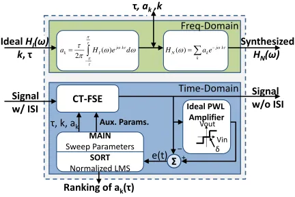
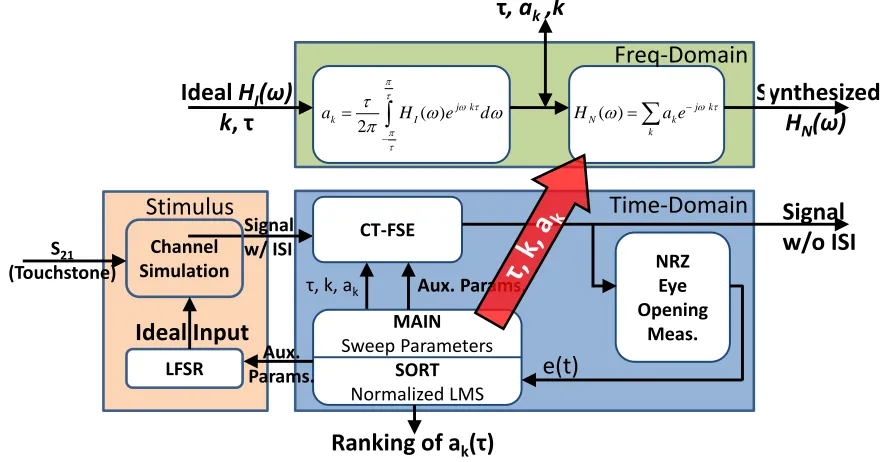
CT-FSE Synthesizer in Matlab
The CT-FSE synthesizer4 (Figure 3.9) is a group of Matlab programs that analyze
CT-FSE parameters and synthesize the CT-CT-FSE filter response in both frequency-domain and
time-domain.
The upper block of Figure 3.9 shows the frequency-domain function of this CT-FSE
synthesizer. It is implemented by coding the CT-FSE pair from (3.7) and (3.14) into Matlab,
also accounting for the non-ideality of the parameters, such as finite k. Furthermore, this
Matlab program allows the behavioral characterization of the CT-FSE system. For example,
the plots in Figure 3.6 and Figure 3.7 demonstrate the influence of τ on CT-FSE response.
The lower block of Figure 3.9 shows the time-domain function of CT-FSE synthesizer.
Besides the most straightforward function of direct processing waveform through CT-FSE
algorithm in time-domain, it is also capable of parameter optimization, including k, ak, and τ.
Sometimes the target ideal filter response, HI(ω), is not readily available, especially in ACCI,
![Figure 1.1. CMOS scaling trends and bandwidth gap [5].](https://thumb-us.123doks.com/thumbv2/123dok_us/1304425.1163064/19.612.93.532.133.335/figure-cmos-scaling-trends-and-bandwidth-gap.webp)
![Figure 1.2. Cross-section of a capacitive coupling interface with high-k under-fill [15]](https://thumb-us.123doks.com/thumbv2/123dok_us/1304425.1163064/20.612.213.406.517.616/figure-cross-section-capacitive-coupling-interface-high-k.webp)