National Conference on 'Innovative Research on Robotics, Circuits and Technology' (IRCT 2018) Organized By : CIrcuit Branches of SCSVMV, (EEE, ECE, EIE & Mechatronics) , Kanchipuram, Tamil Nadu, India
In Assotiation with International Journal of Scientific Research in Science, Engineering and Technology © 2018 IJSRSET | Volume 5 | Issue 1 | | Print ISSN: 2395-1990 | Online ISSN : 2394-4099
Embedded System Design Processor using GAA
J. VinothKumar
Research Scholar, Department of ECE, SCSVMV, Kanchipuram, Tamil Nadu, India
ABSTRACT
Electronics system design is the evolutionary task which is concentrating on the system design for various things like processor, SoC for real time system, embedded systems, reconfigurable system design and more where the Processor design is one of them; it may be a single core, or more than one cores depends on the requirement Specification. There are various hardware description languages used to design and fabricate the processor, among them Verilog, VHDL, SystemVerilog and Bluespec System Verilog are few of them. Bluespec is the one of the modern hardware synthesizable language with guarded atomic action(GAA), which has many advantages over the others. This paper presents the design and implementation of pipeline based 64-bit processor using bluespec, also presents the analysis of number of clock cycles per instructions, implementation of RISC V instruction sets and working principle of pipeline processor using bluespec.
Keywords: Processor, Hardware Description Language, bluespec, Pipeline, Register Files, RISC V, Instruction Set Architecture.
I.
INTRODUCTIONDigital electronics circuits design is ever increasing field in all the technology. In that Integrated Design(IC) design is the one of the important and challenging task in the electronics field. The IC’s can be used in many areas like Digital signal processing, computer architecture system, SoC, embedded systems and robotics architecture etc. An important task of computer architecture is the design of the instruction sets for the processor [4]. Processor design is the complex task involving in most of the modern hardware designer. There are two general types of instruction set architecture for processor design perspectives; one is CISC and another is RISC, each one has its own advantages and disadvantages. CISC has more number of instruction sets, slower clock speed, little general purpose register, more addressing modes and others[2][4]. In today’s technology RISC processors are playing important role, because of simple and reduced instruction sets, shorten the
execution time by reducing the clock cycle per instructions, it can address enormous amount of memory and more general purpose register in term of register files[2].
more. Processor design using the language like Verilog, SystemVerilog, and VHDL may have less flexibility in all aspects for example register files, loading instructions, pipeline concept implementation and many more. But in Bluespec, including the above mentioned and Atomic Transactions Control-Adaptive Parameterization Modern, High-Level Language Facilities, Mainstream Technologies are the key advantages [1][5][6].
Pipeline processor design is another new trend to design processor in such a way that to increases the throughput and efficient handling of data, instructions. These features could be implemented efficiently using bluespec[5],[6].
The proposed work has the following module; 1). Test Bench, 2). Load the instructions in to register files, 3). Perform all operations through pipeline concepts, 4). Write the result into data register files. The working principles will be explained in the later chapters.
II.
RELATED WORKSIn [7] Rakesh M.R has implemented 9 bit RISC processor using pipeline concepts with various blocks including fetch, decode, execute and store the data. He used separate data and instruction memory. He used Verilog and Modelsim for programming and simulation respectively. The advantages of this method are to execute one instruction cycle for 4 stage pipeline.
In [8] Navneet kaur et al, they proposed 64 bit RISC processor desing using VHDL. VHDL programming language is used to develop the RISC in Xilinx 14.2 ISE design suit and functionality simulated on Modelsim 10.1 b simulator. They tested 33 instructions are functionally verified. In device utilization report the number of slices are 34%, Number of Slice Flip Flops 3%, Number of 4 input LUTs 24%, minimum period is found 1.862ns, maximum frequency 539.913MHz, minimum input arrival time before 111.930ns, maximum output required time after clock 9.408ns and it uses 64 bit for
both data bus and address bus. it achieves optimized result.
In [9] Imran Mohammad et al had given a proposal to implement 64-bit RISC processor design and verified with Xilinx simulator. It also presents architecture, data path, and instruction sets of the RISC processor. It can address up to 16 Exabyte’s. They declared that it can be used in many applications like robotics workshop, gaming kits and ATMs.
They tested with 33 instructions and could be implemented for more number of instructions for future works.
In [10] P. Devi Pradeep proposed 64 bit RISC processor design for industry automation and tested with BUT-Built under test. They used collection of registers, instruction commands, 64 bit data and address bus to handle data and addresses. They used Verilog HDL simulator to implement this processor and it capable of perform JUMP, SKIP and HALT instructions. It consumed 18080.18uw.
In [11] Nirav Dave proposed a designing a reorder buffer using bluespec. it synthesized high level description in the form of guarded atomic actions GAA into high quality structural RTL. This paper explores the design of reorder buffer for an out-of – order super scalar processor with MIPS I ISA.
III.
BLUSEPC AT A GLANCEa). Bluespec Syntax
Bluespec has it own syntax; for example module, rules,registers could be used to represents circuits in Bluespec. it wraps around an actual verilog module or a standard module with state elements including other module, rule and interfaces[11],[1]. All the state elements such as registers, flip flop, clocks, memories and others are included in the module. The behaviours can be represented in the form of rules which consists of change of state on the hardware state of the module action and condition required for the rule to be a valid one[11],[1]. The interfaces could be used to communicate with outside world to intereact between modules. Each inteface has guard which restricts when should the method may be called and what should not be called. This method may be any kind of operation like read, write or both. There are three kind of methods[12],[1] they are Value, Action and ActionValue; Value which is return a value to the caller, and have no actions that is when these methods are called, there is no change of state, no side-effect. Action which cause actions that is state changes to occur. ActionValue couples action and Value methods , causing an action to occur and they return a value to the caller[12].
Package pack1
// import sytatemtns
Import package2……… Module mkTb(interfacename) Rule rule1( conditions)
rule implementations… Endule
Rule rule2( conditions)
Rule implementation……….. Endule
……….
Method implementation here ………
Endmodule
EndPackage
Package pack2
// import sytatemtns ………
Module mkTb(interfacename) Rule rule1( conditions)
……….. Endule
Rule rule2( conditions) ………….
Endule ……….
Method implementation here ………
Endmodule
EndPackage
b).Guarded Atomic Transactionsin Bluespec
Hardware should work high efficiency in atomic or independent, an atomic transaction is the core of the hardware design technology. Atomic transactions simplify complex concurrency, improve the communication between modules, and elevate the description and synthesis of system, control [12]. Bluespec[12][1] is the only technology providing such a solution and also it provide hardware modeling, verification and rapid prototype design[13].
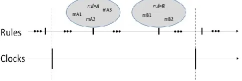
The bluespec also has concurrent rule execution and scheduling rules into clocks [13]. To get maximum performance of any operations using bluespec, we might use to execute many rules as possible concurrently [12]. In BSV, we abstract out the hardware-specific constraints into a simple semantic model of scheduling constraints on pairs of methods.
The above image shows, how more than one rules executing from many methods concurrently that means many rules running within a single clock [13].
IV.
RISC V INSTRUCTIONSThe following are the RISC V instructions and its binary code for processor developments [15].
Figure 2. RISC V instruction types [15]
In this work we have used the following instructions for implementation of the pipeline processors [15].
Instructions Opcode(7)
JAL rd,imm 1101111 LW d,rs1,imm 0000011 SWrs1,rs2,imm 0100011 ADDI rd,rs1,imm 0010011 SLTI rd,rs1,imm 0010011 XORI rd,rs1,imm 0010011 ORI rd,rs1,imm 0010011 ANDI rd,rs1,imm 0010011 SLLI rd,rs1,shamt 0010011 ADD rd,rs1,rs2 0110011 SUB rd,rs1,rs2 0110011 SLL rd,rs1,rs2 0110011 SLT rd,rs1,rs2 0110011 XOR rd,rs1,rs2 0110011 OR rd,rs1,rs2 0110011 AND rd,rs1,rs2 0110011
SD rs1,rs2,imm 0110011 MUL rd,rs1,rs2 0110011 DIV rd,rs1,rs2 0110011
Figure 3. RISC V instruction equivalent codes
DESING AND IMPLEMENTATION OF PIPELINE PROCESSIR
a).Pipeline Processor Architecture
Figure 4. Five stage pipeline Architecture [14]
b). Implementation steps
The proposed method consists of the following components
Test bench
Main package
parameter declarations
Instructions format
Instructions implementations
shows the format in which the input are provided to the main function, this could be designed in instruction format unit having syntax as follows.
Figure 5. Instructions given through test bench
The above Figure 5 shows the arithmetic units having definition of each instruction to be stored. Here we used enum[13],[12] keyword to design instructions for example from the above diagram we can represent binary value for ADD is 00000, SUB is 00001, SLL is 00010 etc.. These values can be used when we are going to decode the instructions.
Figure 6. Arithmetic instructions type definition
Figure 6. shows the parameter declarations section which is used to declare all the parameter used for the
entire pipeline processor design for example data length, address length in terms of bits. This file could
be imported wherever we need it.
Figure 7. Predefined variables
Instruction decode stage will decode the instructions which is after reading instruction from the FIFO line based on the instruction you are passed from test bench. It will read the instruction, extract the bits, assign into the variables and return the result into the main FIFO stage, and then this could be used for input to the next stage through FIFO. For example the pseudo code used in the FIFO pipeline stage is shown.
Rule fetch_stage (condition) FIFO.first
Call fetchinstruction
FIFO1.enq(fetched_instructions) endrule
Rule Decode_stage (condition) FIFO1.first
Call decode(fetched_instruction) FIFO2.enq(decoded_instructions) endrule
Rule MemoryAccess_stage (condition) FIFO2.first
Call
MemoryAddress_calculation(decoded_instru ction)
FIFO3.enq(calculated_address) endrule
Rule execute_stage (condition) FIFO3.first
Call Execute (calculated_address) FIFO4.enq (executed_value) Endrule
Rule execute_stage (condition) FIFO4.first
Call write_back(executed_value) Endrule
b). Pipeline Processor desing and its Stages
many rules and each rule is to perform certain task. Here there are five stages of operations were implemented using FIFO concepts.
Figure 4 show the five stage processor design which is having program counter to count the number of instruction to be performed, clock register is used to count the number of clock pulse is needed to complete in one stage. Each pipeline stage has its own register to store the intermediate result after each stage to be executed. For example IF register can be used to store the fetched instruction to be stored, ID is used for decoded instruction to be stored, MEM this register can be used to store the calculated address, EX register can be used to store the executed result to be stored and finally WB register can be used to store write the result in to registers.
c). Execution and Simulation result
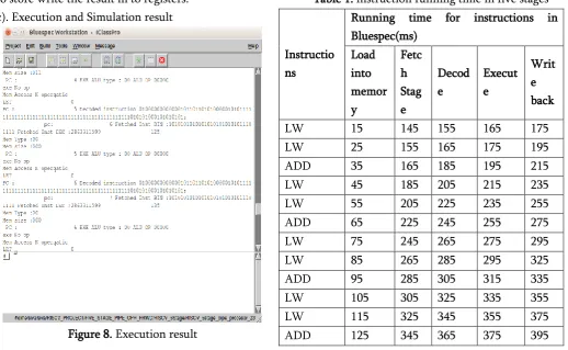
Figure 8. Execution result
Simulation Results
The following section discuss about the analysis of pipeline processor execution result in terms of time taken to load instruction in to the register file, time taken from the register file to fetch stage, time taken to decode the each instruction, execution time of each instruction and write back time. From the table 1. We can understand that the loading instruction in to the
register files will take 15 ms for every instruction and for other operation like fetch, decode execute will take incrementally 15 ms, but for execute to write back instruction will take some different time variations, why because there may be falling in bubbles in between the these instructions. The bubbling time can be reduced through some different way. Through the guarded atomic transactions we could able to reduce the bubbling in the pipeline stages. If we increase the no of stages will lead the increase the throughput. But for some instruction like JUMP, HALT etc will not require execute time so there is bubble formed the subsequent instruction to be executed.
Table 1. instruction running time in five stages
Instructio ns
Running time for instructions in Bluespec(ms)
Load into memor y
Fetc h Stag e
Decod e
Execut e
Writ e back
LW 15 145 155 165 175 LW 25 155 165 175 195 ADD 35 165 185 195 215 LW 45 185 205 215 235 LW 55 205 225 235 255 ADD 65 225 245 255 275 LW 75 245 265 275 295 LW 85 265 285 295 325 ADD 95 285 305 315 335 LW 105 305 325 335 355 LW 115 325 345 355 375 ADD 125 345 365 375 395
reusability often makes more convenient for the hardware designer to utilize the same modules for different functionality.
V.
CONCLUSIONThis work presents the design and implementation of 64-bit RISC V processor using pipeline concepts using bluespec. In this work we have implemented about 40 instructions and the performance of the processor in terms of loading time, instruction in each stages and its execution time were tabulated and analyzed. In this work we have used RISC V 32 bit and 64- bit (extended version) instructions, which is simple to implement. Through the guarded atomic transaction we have achieved better performance. We are concentrated on number of clocks to be reduced for each instruction. We have left some of the work like reducing bubbles in pipeline stage, reorder buffer, instruction and data parallelism could be performed in future.
VI.
REFERENCES[1]. http://www.bluespec.com/technology.html [2]. Tariquzzaman , Syed Rizwan Ali , Nahid Kausar
FPGA implementation of 64 bit RISC processor with Vedic multiplier using VHDL, IOSR Journal of Electrical and Electronics Engineering (IOSR-JEEE) e-ISSN: 2278-1676, p-ISSN: 2320-3331 PP 12-16
[3]. Manju Rani Harpreet Vohra Design and Implementation of 64-Bit Execute Stage for VLIW Processor Architecture on FPGA International Journal of Electronics Communication and Computer Technology (IJECCT) Volume 2 Issue 4 (July 2012)
[4]. Kirat Pal Singh and Shivani Parmar ”Vhdl Implementation of a MIPS – 32 Pipeline Processor” International Journal of Applied Engineering Research, ISSN 0973 – 4562 vol. 7 No. 11. 2012
[5]. Shankar Kumar Mishra, Dr. Nisha P Sarware “Review of 5 stage Pipelined Architecture of 8
Bit Pico Processor”, International Journal of Electronics, Communication & Soft Computing Science and Engineering, ISSN: 2277-9477, Volume 3, Issue 4
[6]. Navneet kaur , Adesh Kumar , Lipika Gupta VHDL Design and Synthesis of 64 bit RISC Processor System on IOSR Journal of VLSI and Signal Processing (IOSR-JVSP) Volume 3, Issue 5 (Nov. – Dec. 2013)
[7]. Rishiyur S. Nikhil and Kathy Czeck BSV by Example, The next-generation language for electronic system design Revision: November 3, 2010
[8]. Arvind et al,Computer Architecture: A Constructive Approach Using Executable and Synthesizable Speci_cations 2012-2013
[9]. Rakesh M.R ,RISC Processor Design in VLSI Technology Using the Pipeline Technique, INTERNATIONAL JOURNAL OF INNOVATIVE RESEARCH IN ELECTRICAL, ELECTRONICS, INSTRUMENTATION AND CONTROL ENGINEERING Vol. 2, Issue4, April 2014.
[10]. Navneet kaur , Adesh Kumar , Lipika Gupta VHDL Design and Synthesis of 64 bit RISC Processor System on Chip (SoC) IOSR Journal of VLSI and Signal Processing (IOSR-JVSP) Volume 3, Issue 5 (Nov. – Dec. 2013)
[11]. Imran Mohammad , Ramananjaneyulu K, FPGA Implementation of a 64-Bit RISC Processor Using VHDL International Journal of Reconfigurable and Embedded Systems (IJRES) Vol. 1, No. 2, July 2012
[12]. P. Devi Pradeep and D.Srinivasa Rao Design and Implementation of 64-Bit RISC Processor for Industry Automation International Journal of u- and e- Service, Science and Technology Vol.8, No.1 (2015), pp.427-434
[14]. Rishiyur S et al, BSV by Example The next-generation language for electronic system design Revision: November 3, 2010
[15]. Arvind et al, Computer Architecture: A Constructive Approach Using Executable and Synthesizable Specifications December 31, 2012 [16].
http://cse- wiki.unl.edu/wiki/index.php/CSE430/830-2011SpringTeamB
![Figure 4. Five stage pipeline Architecture [14]](https://thumb-us.123doks.com/thumbv2/123dok_us/1233374.1628265/4.595.303.555.170.376/figure-five-stage-pipeline-architecture.webp)