Novel Design of n-bit Controllable Inverter by Quantum-dot
Cellular Automata
M. Kianpour
1, R. Sabbaghi-Nadooshan
21- Electrical Engineering Department, Islamic Azad University, Science and Research Branch, Tehran, I. R. Iran
2- Electrical Engineering Department, Islamic Azad University, Central Tehran Branch, Tehran, I. R. Iran
(*) Corresponding author: [email protected]
(Received: 22 Jan. 2014 and accepted: 09 Feb. 2014)
Abstract:
Application of quantum-dot is a promising technology for implementing digital systems at nano-scale. Quantum-dot Cellular Automata (QCA) is a system with low power consumption and a potentially high density and regularity. Also, QCA supports the new devices with nanotechnology architecture. This technique works based on electron interactions inside quantum-dots leading to emergence of quantum features and decreasing the problem of future integrated circuits in terms of size. In this paper, we will successfully design, implement and simulate a new 2-input and 3-input XOR gate (exclusive OR gate) based on QCA with the minimum delay, area and complexities. Then, we will use XOR gates presented in this paper, in 2-bit, 4-bit and 8-bit controllable inverter in QCA. Being potentially pipeline, the QCA technology calculates with the maximum operating speed. We can use this controllable inverter in the n-bit adder/subtractor and reversible gate. Keywords: Exclusive OR(XOR) gate, Inverter, Majority gate, Quantum-dot Cellular Automata(QCA).
Int. J. Nanosci. Nanotechnol., Vol. 10, No. 2, June 2014, pp. 117-126
1. INTRODUCTION
Quantum-dot Cellular Automata (QCA) is a promising model emerging in nanotechnology. In QCA, binary data appear as loading quantum-dots
within the cells. XOR gates are important circuits in
QCA technique because they are expected to be used in adder and reversible gate at nano-scale. QCA is a
known technology that can be a good replacement
for CMOS-based devices in nano-scale.
After decades of its final growth the minimum feature in CMOS technology, is ultimately confronted with
limitations. In QCA, binary data appear as loading
quantum-dots within the cells. Numerous studies are reported in which QCA is able to produce devices with high density, low power consumption and very high switching speed.
QCA was first proposed by Lent et.al in 1993 [1], and
was developed in 1997 [2]. It is expected that QCA
plays an important role in nanotechnology research.
Due to significant features of QCA, high density, low power consumption, very high processing potential
and being pipeline, it has become an interesting alternative for CMOS technology. Using molecular
QCAs we can have a density higher than 100 devices
(~3×10¹¹ – 18nm cells) per cm2 and a performance
faster than 2.5 THz. Theoretically, processing speed may reach 25 THz [1].
In this paper we concentrate on designing,
implementing and analyzing a basic device in QCA and use it in one of the most fundamental circuits in QCA. Designing method in QCA is different
from the CMOS so that we will use quantum cells
in QCA as transistor in CMOS technology. In this
and delay and complexity. This 2-input XOR gate is
used in designing a controllable inverter, and finally using this 3-input XOR gate, we can design a double
controllable inverter.
We follow two objectives in our designs: 1. Implementation with the minimum complexity and number of cells; 2. Simplification of connections
and decreasing delays and consequently increasing processing speed. Designing a 2-bit controllable
inverter is the less studied new technology. It can also be generalized to 4, 8 and higher bits. Most of
previous studies have been conducted on XOR gate. Several QCA-based XOR designs have been
proposed in [3, 4]. Tougaw et al.
[3] present the design of basics quantum-dot
cellular automata (QCA) XOR gate. Mustafa et al.
[4] present novel design of quantum-dot cellular
automata (QCA) XOR gate. Each of the XOR gate
[3, 4], has an inordinate latency and very complex
circuit.
The noise coupling problem is solved by arranging
the QCA cells and assigning the clocking zones in such a way, that unwanted signal coupling is
diminished, resulting in implementation requiring only one layer of QCA cells (including all the logic and interconnection).
Robust operation is achieved with very high clock frequencies, verified by the time-dependent
simulation of the QCADesigner bistable engine.
Furthermore, we have used 2DDwave clocking method [5] that led to decreased delay and increased
operating speed in circuit. This controllable inverter
circuit is applicable in the n-bit adder/subtractor and reversible gate [6-7].
This paper is organized as follows: section 2 reviews
the QCA. In section 3, the design and architecture of
2-input and 3-input XOR gate in QCA are shown. 2, 4 and 8-bit controllable inverter implementation in QCA are also presented in section 4. In section 5, simulation results are shown. Finally, we conclude
the paper in the last section.
2. QCA REVIEW
2.1. Background
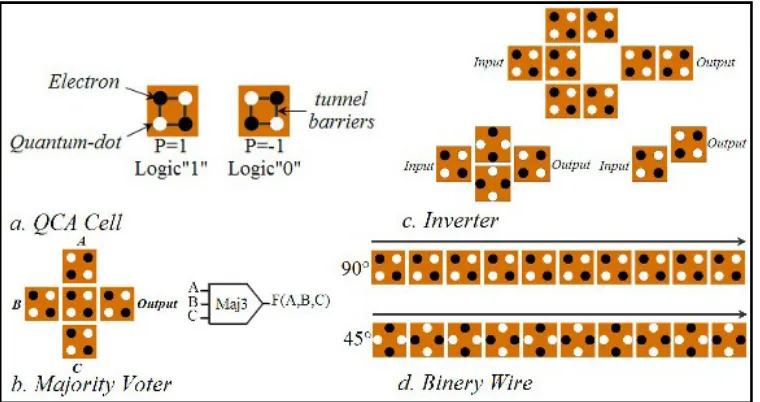
The main units of QCA are QCA cells located on the vertices of a square by four quantum-dots. There
are two electrons in each cell which can be located,
according to Coulomb electrostatic interaction, in diagonal position. The electrons are controlled by potential barriers and can move by tunneling and controlling the potential barriers and produce our binary values.
It is assumed that tunneling to outside the cells is impossible due to large potential barriers. Binary
data can be encoded in two possible polarizations (1,-1) so that 0, 1 will respectively produce our binaries in QCA, as observed in Figure 1(a). If two
cells are located beside each other, the Coulomb
interaction between the electrons causes the cells
to have equal polarization and an equal amount of their left side cell. The most fundamental logical gate in QCA is majority gate. A logical equation for a majority gate is:
F(A,B,C)=AB+AC+BC
It is implemented by five QCA cells as shown in Figure 1(b). If we keep the polarization of one of the majority gate inputs constant on 1 or 0, we will
obtain OR and AND gates, respectively. Another high-consumption and important gate in QCA
is NOT or inverter gate. Two common and new
examples of such gates are presented in Figure 1(c).
Having AND, OR and NOT gates, we are able to
design and implement the most complex logical circuits. In Figure 1(d) a number of QCA cells are
located next to each other creating a wire in QCA.
This wire is of two types: 45 and 90 degrees, which are applicable in cross over [8-10].
2.2. QCA clocking
All proposed circuits in QCA not only need a clock to synchronize and control information flow but also this clock provides the necessary power to
run the circuit. QCA calculations by tunneling are
performed by four phases of clock signal, as you observe in Figure 2. Clocking in QCA includes four phases: hold, release, relax and switch. Each phase is 90 degrees behind the other.
During switch phase, the potential barriers among quantum dots raise gradually and QCA cell will
be located in one of the existing polarization states
with regard to the adjacent cell. During hold phase, the barriers between quantum-dots remain at their
higher levels preventing tunneling of electrons, and
polarization of QCA cells will remain the same.
During release and relax phases, the barriers
between quantum-dots reduce to its minimum value Figure 2: Four phases of the QCA clock, (b) Clock zones signal.
in relax phase and the electrons will be able to move within the cell. The clock signal can be produced by an inducer electric field and is embedded under the lower surface of QCA by CMOS wires [5, 11-12].
QCADesigner is a tool generally used for simulating the QCA circuits. A QCA model might be of single layer or multi layer. In a single layer design, only
normal cells, rotate cells and fix polarization cells are used. These findings are depicted in Figure 3(a), 3(b) and 3(e). When a QCA signal moves from one
layer to another, it goes via vertical cells (Figure 3(c)).Then, in the upper layer, it propagates through cross over cells (Figure 3(d)). Finally, it can go
down to the main layer via vertical cells [13].
3. ARCHITECTURE OF PROPOSED
2-INPUT AND 3-INPUT XOR GATE IN QCA
In this article, we have designed a hierarchical circuit. First, we designed a 2-input XOR and then the 3-input XOR. With a series connection of this XOR we produced the inverter of the n-bit digits with control lines.
3.1. 2-input XOR gate in QCA
The 2-input XOR gate in the logic mode has the
following function: if two input lines have the
same amounts, the output value becomes “0” and
if two input lines have different values, the output
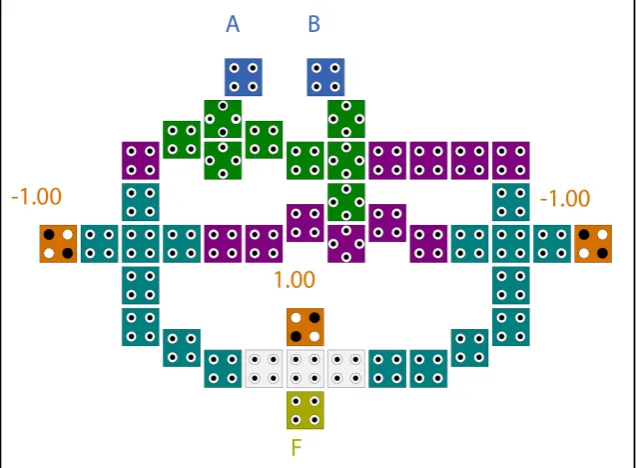
equals to “1”. Therefore, this gate has diverse and extensive functions in different circuits. Figure 4(a) exhibits logic implementation of 2-input XOR gate and Figure 4(b) exhibits the proposed 2-input XOR gate implementation in QCA technique.
Figure 4: 2-input XOR gate implemented by (a) logical gate, (b) QCA with majority gate.
This gate bears the logic equation of F(A,B)=A
(
A
,
B
)
A
B
A
'
B
AB
'
F
=
⊕
B=A’B+AB’=
+
The circuit was designed and simulated for
functional behavior using the QCADesigner Ver.
2.0.3. In the bistable approximation, the following parameters were used: Number of samples = 50000, Convergence tolerance = 0.001, Radius of effect = 65nm, Relative permittivity = 12.9, Clock high =
9.8e-022, Clock low = 3.8e-023, Clock shift = 0, Clock amplitude factor = 2, Layer Separation=11.5, Maximum iteration per sample = 100.
Implementation of 2-input XOR gate in QCA has
been exhibited in Figure 5, which was implemented
by the minimum cell number and complexity and
reached the output in one clock cycle.
The proposed 2-input XOR gate consists of 45 cells covering an area of 0.05 μm2 (278nm×178nm). The simulation results of the 2-input XOR gate is presented in Figure 6.
3.2. 3-input XOR gate in QCA
The 3-input XOR gate is a combinational circuit producing the arithmetical XOR of three bits. This circuit includes three inputs and one output. Here,
we will implement our 3-input XOR using two 2-input XOR. Two input variables indicated with A and B are connected to the first-stage of XOR gate. The third input C is lower value and connected to the
second-stage of XOR gate. The 3-input XOR gate in
the logic mode has the following function: if three
input lines have same amounts, the output value
becomes “0” and if two input lines have “0” values, the output equals “1” and if two input lines have
“1” values, the output equals to “0”. Therefore, this gate has diverse and extensive functions in different
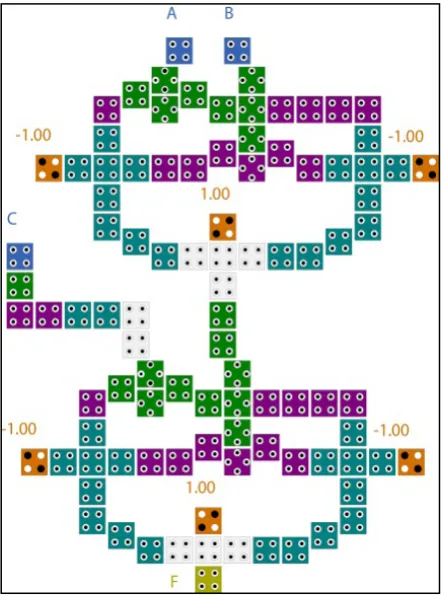
circuits. Figure 7(a) exhibits logic implementation of 3-input XOR gate and Figure 7(b) exhibits the
proposed 3-input XOR gate implementation in QCA technique.
This gate bears the logic equation of
And has a truth table as per Table I.
Table I: Truth table of the 3-input exclusive OR(XOR) gate
C A B F(A,B,C)
0 0 0 0
0 0 1 1
0 1 0 1
0 1 1 0
1 0 0 1
1 0 1 0
1 1 0 0
1 1 1 1
Implementation of 3-input XOR gate in QCA is
exhibited in Figure 8, which was implemented
by the minimum cell number and complexity and
reached the output in two clock cycles.
Figure8: 3-input XOR gate implemented in QCA.
The proposed 3-input XOR gate consists of 98 cells covering an area of 0.13 μm2. The simulation results
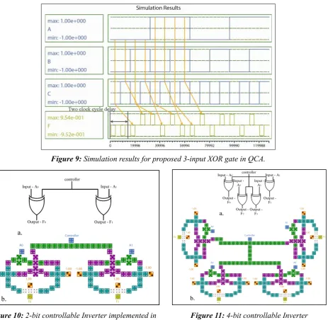
of the 3-input XOR gate is presented in Figure 9.
4- CONTROLLABLE INVERTER
IMPLEMENTATION IN QCA
The controllable inverter is a combinational circuit
which performs arithmetic operations i.e. inverted the binary digits. In this paper, we have designed a hierarchical circuit. First, we designed a controllable inverter based on 2-input XOR gate. With a series connection of two or four 2-input XOR gate, we
obtained the inverted of 2 and 4-bit. Then, the
controllable inverter circuit was made by 3-input XOR gate. We have designed 2 and 4-bit double controllable inverter with 3-input XOR gate in QCA.
4.1. Controllable inverter implementation with 2-input XOR gate in QCA
In order to implement controllable inverter circuit,
we used the proposed 2-input XOR gates and
2-input XOR gate features in inverter operations. In
the first state, two 2-input XOR gates were located next to each other. Then we connected one of the input gate pins to two input data, and other pins were connected to each other and used as controller input. In this circuit, if the control input was loaded
on zero, the output remained the same value, and if
the control input was loaded on one, the output was
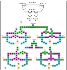
inverted. The layout of 2-bit controllable inverter in QCA is presented in Figure 10.
In the second state, four 2-input XOR gates were located next to each other. Then we connected
one of the input gate pins to four input data, and
other pins were connected to each other and used
as control input. The layout of 4-bit controllable inverter in QCA is presented in Figure 11.
4.2. Double controllable inverter implementation with 2-input XOR gate in QCA
In order to implement double controllable inverter
circuit, we used the proposed 3-input XOR gates and
3-input XOR gate features in inverter operations. In
Figure 9: Simulation results for proposed 3-input XOR gate in QCA.
Figure 10: 2-bit controllable Inverter implemented in
QCA. Figure 11: implemented in QCA.4-bit controllable Inverter
next to each other. Then we connected one of the input gate pins to two input data, and twin other pins were
connected to each other and used as controller input.
In this circuit, if the two control input was loaded on “00 & 11”, the output remained the same value, and if the control input was loaded on “01 & 10”, the output was inverted. The layout of 2-bit double controllable
inverter in QCA is presented in Figure 12.
Generalizing this 2-bit double controllable inverter provided only requires a driver circuit. For example,
if we want a 4-bit double controllable inverter
implementations, we need four, 3-input XOR gates. This 4-bit double controllable inverter will attain the output in the three clock cycles.
5. SIMULATION RESULT
In our design we used QCADesigner Ver. 2.0.3 in
the bistable approximation. Table II, presents a brief description for each parameter used for a simulation
Figure 12: 2-bit double controllable Inverter implemented in QCA.
Figure 13: Simulation results for proposed 2-bit
Table III: Simulation result of proposed new circuits in QCA
Area
(µm2) Complexity (# Cell) Delay (10-12s in 1 THz)
proposed 2-input XOR gate 0.05 45 1
2-input XOR gate in [3] 0.06 64 unknown
2-input XOR gate in [4] 0.07 44 1
3-input XOR gate 0.13 98 2
2-bit controllable Inverter 0.16 106 1
4-bit controllable Inverter 0.37 218 1
2-bit double controllable Inverter 0.31 219 2
Table II: Parameters model in QCADesigner simulator
Parameter Value
Cell width 18nm
Cell height 18nm
Dot diameter 5nm
Number of samples 50000 – 1000000
Convergence tolerance 0.001
Radius of effect 65nm
Relative permittivity 12.9
Clock high 9.8e-22J
Clock low 3.8e-23J
Clock amplitude factor 2
Layer Separation 11.5nm
Maximum iteration per sample 100
Figure 15: Simulation results for proposed 2-bit double controllable inverter in QCA.
In Table III, we made a comparison of area (µm2), complexity (number of cells), delay (10-12s in 1THz) and
power consumption in proposed new circuits in QCA.
Figure 13 illustrates simulation of 2-bit controllable
Inverter which came to the output with a four clock phase delay. However, Figure 14 shows the simulated 4-bit controllable Inverter which reached the output by four clock phase delay.
Figure 15 shows simulation result of proposed 2-bit
double controllable Inverter. In this simulation, the
results reached output correctly, after two clock
6. CONCLUSION
We have proposed a new extendable design of
2-input and 3-input XOR gate in QCA technique. Using proposed XOR gates in this paper, the 2-bit and 4-bit controllable Inverter and 2-bit double controllable Inverter gates have been designed and
implemented with minimum delay, complexity
and area in QCA. This controllable Inverter may
be used for reversible gate or adder/subtractor for implementations with inverted circuit, which
considering the pipeline is of QCA, the operational
speed will be high and the consumption power and the delay will be very low.
REFERENCES
1. C.S. Lent, P.D. Tougaw, W. Porod and G.H. Bernstein: Nanotechnology., Vol. 4, No. 1, (1993), pp. 49–57.
2. I. Amlani, A. Orlov, G.H. Bernstein, C.S. Lent and
G.L. Snider: Science., Vol. 227, No. 5328, (1997), pp. 928–930.
3. P. Douglas Tougaw, Craig S. Lent: journal of applied physics, Vol.75, No.3, (1994), pp. 1818-1825.
4. M. Mustafa, M.R. Beigh: Indian Journal of Pure & Applied Physics., Vol.51, No.1, (2013), pp. 60-66.
5. M. Momenzadeh, J. Huang and F. Lombardi.
Chapter 3 and references therein, Boston, Artech
House., (2008).
6. H. Cho, E.E. Swartzlander: IEEE Transactions on Nanotechnology., Vol.6, No.3, (2007), pp. 374–384.
7. M.B. Tahoori, M. Momenzadeh, J. Huang, F.
Lombardi: Transactions on Nanotechnology., Vol.3,
No.4, (2004), pp. 432–442.
8. I. Amlani, A.O. Orlov, G. Toth, G.H. Bernstein, C.S.
Lent and G.L. Snider: Science., Vol. 284, No. 5412, (1999), pp. 289–291.
9. G. Toth and C.S. Lent: Journal of Applied Physics.,
Vol. 85, No. 5, (1999), pp. 2977–2984.
10. H. Cho and E.E. Swartzlander: IEEE Transactions on Computers., Vol. 58, No. 6, (2009), pp. 721–727.
11. R. Landauer: IBM J. Res. Develop., Vol. 5, No. 3, (1961), pp. 183–191.
12. C.S. Lent and P.D. Tougaw: Proceedings of the IEEE., Vol. 85, No. 4, (1997), pp. 541–557.
13. J. Timler, C. S. Lent: journal of applied physics.,
Vol.91, No.2, (2002), pp. 823-831.
14. K. Walus, T. Dysart, G. Jullien, R. Budiman: IEEE