© 2017 AJAST All rights reserved. www.ajast.net
Design of Power Efficient 4x4 Multiplier Based On Various Power Optimizing
Techniques
A.Venkatesh
1, N.Rathan
2and R.Saranya
31Assistant Professor, Department of Electronics and Communication Engineering, Hindusthan Institute of Technology, Coimbatore, India. 2Assistant Professor, Department of Electronics and Communication Engineering, Hindusthan Institute of Technology, Coimbatore, India. 3Assistant Professor, Department of Electronics and Communication Engineering, Hindusthan Institute of Technology, Coimbatore, India.
Article Received: 21 February 2017 Article Accepted: 11 March 2017 Article Published: 13 March 2017
1.INTRODUCTION
The purpose of low power electronics is to compress complex electronic circuits in minimum area with reduction in power dissipation and delay. The power requirements of these devices have increased many folds with the increase in complexity of ICs. The need of transistors in VLSI design is duly elucidated by Moore’s Law [1]. Reducing the transistor count and power of circuits have been focus of researchers for so many years and is still continuing [2]. Now-a-days logic circuits are designed using pass transistor logic techniques [3]. Recently many techniques have been proposed with the objective of improving speed and power Consumption. The Double Pass-Transistor Logic, developed by Hitachi demonstrated a 1.5ns, 32-bit ALU in 0.25μm CMOS technology and 4.4ns, 54X54 bit multiplier. Similarly many works have been done recently to design 4x4 bit multiplier. The main objective of our work is to implement the low power high speed multiplier based on Sleepy Stack & to make a detailed comparative study with conventional CMOS multiplier. Our multiplier uses less number of transistors in comparison to the conventional multiplier; so that the propagation delay time & power consumption gets reduced. It also helps in reducing the layout area thereby decreasing the entire size of a module where this multiplier sub module is used. With the objective of further reducing the POWER a novel design of a Sleepy Stack technique is proposed in the current paper.
2. DESIGN OF 4x4 MULTIPLIER
A combinational multiplier is a superior model Show casing how simple logic functions (gates, half adders and full adders) can be combined to build a much more complex function. Consider the following example (fig. 1) for binary multiplication of two positive 4-bit integer values. Here, each bit in the multiplier is multiplied with the multiplicand. Each of the four products is aligned (shifted left) according to the position of the bit in the multiplier that is being multiplied with the multiplicand.
Here, each bit in the multiplier is multiplied with the multiplicand. Each of the four products is aligned (shifted left) according to the position of the bit in the multiplier that is being multiplied with the multiplicand. The four resulting products are added to form the final result. Therefore for an NxN multiplier, the result is 2N bits wide. With binary numbers, forming the products is much easy. If the multiplier bit is a 1, then the corresponding product is simply an appropriately shifted copy of the multiplicand. If the multiplier bit is a zero, then the product is zero. 1-bit binary multiplication is thus just an AND operation.
Fig.1. Binary multiplication example (4x4)
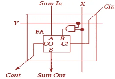
To build the NxN multiplier let us take an array of a building block consisting of an AND gate and a full adder to get the partial product. The building block is shown in fig. 2 and the 4x4 multiplier in fig. 3 correspondingly. The basic building block consists of an AND gate for computing locally the corresponding partial product (X.Y), an input passed into the block from above (Sum In), and a carry (Cin) passed from a block diagonally above. It generates a carry out bit (COUT) and a new sum out bit (Sum Out). Fig. 3 illustrates the interconnection of these building blocks to construct a 4x4 combinational multiplier. The Ai values are distributed along block diagonals, and the Bi values are passed along the rows. A B S T R A C T
In this paper, we propose a new technique for implementing a low power high speed multiplier based on Sleepy Stack Technique and consisting of minimum number of transistors. Multiplier circuits are used comprehensively in Application Specific Integrated Circuits (ASICs). An 4 bit x 4 bit multiplier has also been implemented using the design of only using basic combinational circuits and its performance has been analyzed and compared with similar multipliers designed with peer combinational design available in literature. The explored method of implementation achieves a high speed low power design for the multiplier. Simulated results indicate the superior performance of the proposed technique over conventional CMOS multiplier. Detailed comparison of simulated results for the conventional and present method of implementation is presented.
© 2017 AJAST All rights reserved. www.ajast.net Fig.2. Building block of multiplier
Fig. 3. 4x4 multiplier using AND gate, Half adder and full adder
To design a low power 4x4 multiplier the approach is to design the circuits with minimum nos. of transistors. Here the basic building blocks (half adder, full adder & AND gate) of\ the 4x4 multiplier shown in fig. 3 are constructed with minimum no of transistors which are discussed in section 3.
3. ARCHITECTURE OF 8-T FA, 2-T AND GATE 3-T XOR GATE & 5-T HA
This work presents adder circuits using pass transistor logic based MUX & XOR gate, which contains lesser no. of transistors and achieving better performance. This full adder using pass transistor logic has advantages over CMOS and is characterized by excellent speed and low power. In electronics, Pass-Transistor-Logic (PTL) describes several logic families used in the design of integrated circuits. It reduces the count of transistors used to make different logic circuits, by eliminating redundant transistors. Transistors are used as switches to pass logic levels between nodes of a circuit, instead of as switches connected directly to supply voltages. This reduces the number of active devices, but has the disadvantage that output levels can be no higher than the input level. Each transistor in series has a lower voltage at its output than at its input. For proper operation, design rules define the arrangement of circuits, so that sneak paths, charge
sharing, and slow switching can be avoided. Double Pass transistor Logic (DPL) eliminates some of the inverter stages required for Complementary-Pass-transistor- Logic (CPL) by using both N and P channel transistors, with dual logic paths for every function. While it has high speed due to low input capacitance, it has only limited capacity to drive a load. Pass transistor logic has become important for the design of low-power high-performance digital circuits due to the smaller node capacitances and reduced transistors count it offers. However, the acceptance and application of this logic depends on the availability of supporting automation tools, e.g. timing simulators, which can accurately analyse the performance of large circuits at a speed, significantly faster than that of SPICE based tools.
3.1 8-T Full Adder (FA)
The proposed 2T XOR gate has been used to design a 6T full adder. The two outputs SUM and CARRY (𝐶𝑜𝑢𝑡) can be generated based on the Boolean equations of full adder as follows:
𝑆𝑢𝑚 = 𝐴⨁𝐵⨁𝐶𝑖𝑛
𝐶𝑜𝑢𝑡 = 𝐵.𝐶𝑖𝑛 + 𝐶𝑖𝑛.𝐴 + 𝐴.𝐵 = 𝐶𝑖𝑛. (𝐴⨁𝐵) + 𝐴.𝐵
The logic circuit of typical full adder is given in Figure 4. The exclusive O Ring realized using wired logic of 3T XOR gate as depicted in equation give rise to sum output and the final carry output is given by using M1 and M2 pass transistors given by equation. The W/L ratio of M3 and M4 transistors are W=300 nm, L=60 nm in 65-nm technology. The W and L of transistors from M1 to M4 is same as defined for XOR gates. The schematic of the proposed 8 transistor full adder is shown in Figure 9. A reverse bias voltage of 320 mV is kept in order to concisely represent the appropriate logic high and logic low levels in the output of simulated circuit. Evidently, for the three input combination there is two stages delay for the sum and carry output and the delay for carry output is less than then As two XOR gates are used with reverse bias, there is decline in the logic level with the cascading of exclusive OR gates mainly perturbed at A=1 and B=1. The approach of using minimum width and length is for minimizing the power consumption in the circuit.
Fig. 4. Logic circuit of full adder
© 2017 AJAST All rights reserved. www.ajast.net with 3 transistors as shown in fig.5 below. The second
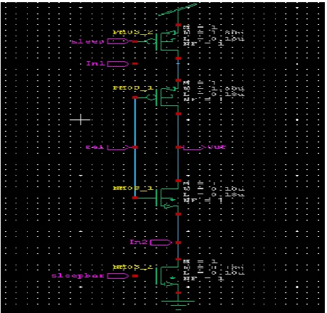
component required to design a full adder with 2 XOR gate to implement the sum out & another two input MUX to implement the carry out. The basic structure of the 2:1 MUX using pass gate transistor logic and implement sleepy stack technique is shown in fig. 8. In this configuration we have connected PMOS and NMOS along with a SEL line, as in MUX.
Fig. 5. Basic view of 3T XOR gate
Fig.6. Basic view of 2T MUX
Sleepy Stack Approach
The sleepy stack technique divides existing transistors into two half size transistors like the stack approach. Then sleep transistors are added in parallel to one of the divided transistors.
Fig.7. Sleepy Stack Approach
Figure 7 shows its structure. During sleep mode, sleep transistors are turned off and stacked transistors suppress leakage current while saving state.
Each sleep transistor, placed in parallel to the one of the stacked transistors, reduces resistance of the path, so delay is decreased during active mode.
However, area penalty is a significant matter for this approach since every transistor is replaced by three transistors and since additional wires are added for S and S‟, which are sleep signals.
It reduces noise and power so we implement the sleepy stack technique in AND gate. For build a more efficient 4x4 multiplier. Basic view of sleepy stack technique using And gate shown in figure.
Fig. 8. Basic view of 2T MUX with Sleepy Stack Approach
Using 2 input MUX & 2 input XOR gate we can design a 8-T FA as shown in fig. 9 below,
Fig. 9. 8-T FA based on MUX & XOR gates
3.2 5-T Half Adder (HA)
© 2017 AJAST All rights reserved. www.ajast.net Fig.10. 5-T HA based 3T XOR & 2T AND
There are three major sources of power dissipation in a digital CMOS circuit: logic transition, short-circuit current and leakage current. The short-circuit current is the direct current passing through the supply and the ground, when both the NMOS and the PMOS transistors are simultaneously active.
As the proposed 8-T FA and 5T HA do not direct connections to or port (voltage connections to the back gate terminals are not considered), the probability of a direct path formation from positive voltage supply to the ground during switching can be substantially reduced that is, and the power consumption due to short circuit current is considered negligibly small.
Furthermore, in the new adder circuits, all of its internal gate nodes are directly excited by the fresh input signals (and), leading to a much faster transition (low rise and fall times) in its output signals. As a result, the power consumption of the following buffer stage can benefit from faster/cleaner Sum and Cout outputs.
4. SIMULATION RESULTS & ANALYSIS
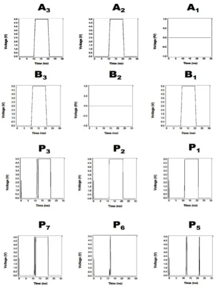
For testing the proposed multiplier we provide the input combinations as bit parameter of example shown in fig. 1. All the combinations are introduced during the time period between 10ns to 20ns.
Thus for the outputs we also concentrate over that particular time period only. We run the simulation over both conventional & proposed two different multipliers architecture. The transient responses of all the circuits are shown below in fig.11 & fig.12 respectively. After running the simulation the power consumption and delay of the circuits are tested and compared.
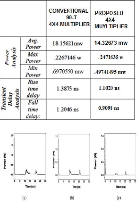
From the simulation it can be easily understood that the proposed multipliers have the same functional response as like the conventional multiplier. The power & timing behaviour is tabulated in the table 1,
Regarding area consideration it can be easily understood that with lesser no. of transistor count compared with conventional circuit multiplier core will be much lower size compared to 10x16-T 4x4 multiplier and 34x16-T CMOS 4x4 multiplier.
Fig. 11 Transient response of 90-T conventional 4x4 Multiplier Ai: one multiplicand input (4 bits), Bi: one multiplier input (4 bits), Pi: partial product
Fig. 12 Transient response of proposed 4x4 Multiplier Ai: one multiplicand input (4 bits), Bi: one multiplier input (4 bits), Pi: partial product.
© 2017 AJAST All rights reserved. www.ajast.net Table 1. Comparison between Conventional & Proposed
Multiplier
Fig. 13. Power consumption of (a) conventional CMOS multiplier; (b) Power consumption of conventional 90-T multiplier and (c) proposed 4x4 multiplier.
5. CONCLUSION
From the above results it can be concluded that our proposed multiplier has got better performance in terms of speed, power and area consideration in comparison with the conventional CMOS multiplier. It turns out that in contrast to older process technologies, this approach is more suitable for industrial usage in advanced process technologies.
REFERENCES
[1] V.Gowrishankar, D.Manoranjitham and P. Jagadeesh, “Efficient FIR filter design using modified carry select adder & Wallace tree multiplier”, International Journal of Science,
Engineering and Technology Research, Vol. 2, pp. 703-711,
March 2013.
[2] Hina Malvina, Sudha Nayar, C.M Roy, “ A New Approach For Leakage Power Reduction Techniques in Deep Submicron Technologies in CMOS circuit for VLSI Applications” International Journal of Advanced Research
in Computer Science and Software Engineering, Volume 3,
Issue 5, May 2013.
[3] Y.Berg, M. Azadmehr, "Novel ultra-low-voltage and high-speed CMOS pass transistor logic", Proceedings of the
IEEE, Faible Tension Faible Consommation (FTFC), Paris,
2012.
[4] A.Daniel Raj, S.Vijayalakshmi, P.Sathyamoorthy, "Efficient Design of 4-bit array multiplier using GDI low power cell", International Journal of Computer Technology and Electronics Engineering (IJCTEE), Volume 2, Issue 6, PP-47-51, December 2012.
[5] Vijayasalini. P, Nirmal kumar. R, Dhivya. S. P, Dr. G.M. Tamilselvan, "Design and Analysis of Low Power Multipliers and 4:2 Compressor Using Adiabatic Logic", International Journal of Emerging Technology and Advanced Engineering, Volume 3, Issue 1, PP-288-292, January 2013.
[6] Shubhajit Roy Chowdhury, Aritra Banerjee, Aniruddha Roy, Hiranmay Saha, “A high Speed 8 Transistor Full Adder Design using Novel 3 Transistor XOR Gates”, International Journal of Electronics, Circuits and Systems, pp. 218, 2008.
[7] N.Anuar, Y. Takahashi, T. Sekine "4×4-bit array two phase clocked adiabatic static CMOS logic multiplier with new XOR", IEEE VLSI System on Chip Conference
(VLSI-SoC), PP-364-368, 2010.
[8] Hung Tien Bui, Yuke Wang and Ying Tao Jiang, “Design and Analysis of low Power 10 Transistor Full adders Using Novel XOR/XNOR gates”, IEEE Transactions on Circuits And Systems- II, : Analog and Digital Signal Processing, Vol.49, No.1, January 2002.
[9] J.C. Park, V. J. Mooney III and P. Pfeiffenberger, “Sleepy Stack Reduction of Leakage Power,” Proceeding of the International Workshop on Power and Timing Modeling,
Optimization and Simulation, pp. 148-158, September 2004.
[10] Clive Maxfield, “Bebop to the Boolean boogie: an unconventional guide to electronics Newness”, 2008, pp. 423-426
[11] Jaume Segura, Charles F. Hawkins “CMOS electronics: how it works, how it fails”, Wiley-IEEE, 2004, page 132.
[12] Yingtao Jiang, Abdulkarim Al-Sheraidah, Yuke Wang,
Edwin Sha, and Jin-Gyun Chung, “A Novel
Multiplexer-Based Low-Power Full Adder” IEEE Transaction on circuits and systems-II: Express Brief, Vol. 51, No. 7,p-345, July- 2004.