Design of High-Speed Parallel Data Interface
Based on ARM & FPGA
Daode Zhang
School of Mechanical Engineering, Hubei University of Technology, Wuhan, 430068, China Email: [email protected]
Yurong Pan and Xinyu Hu
School of Mechanical Engineering, Hubei University of Technology, Wuhan, 430068, China Email: [email protected]
Abstract—This article described a complete design of parallel interface based on ARM & FPGA, using the on-chip DPRAM in FPGA to improve the metastability problem which was generated during data transmission between the
asynchronous clock-domains ;And it achieved the design
of ARM & FPGA hardware interface module , data-sending module , data-receiving module and FPGA driver module , also gave the feasible method that using a flag to solve the
dislocation of data-reading ;Test results indicate that the
system works steadily.
Index Terms— ARM, FPGA, Parallel Data Interface, metastability
I. INTRODUCTION
With the arrival of information age, embedded systems with network connection function have been used widely. At present, ARM-based platform has been widely put into use in many fields of embedded system. FPGA is developing rapidly, depending on its parallelism and reconstruction which much better than other chips, and its application also seeps to many fields. In many kinds of high-speed data interface designs, the way of data acquisition and the speed of transmission are becoming the new challenge [1][2]. It has been a trend that the FPGA+ARM construction become the high-speed digital processing system which fulfills the timely request, and the alternation between FPGA and ARM is becoming more urgent. This paper introduces a high-speed parallel interface design based on ARM + FPGA construction.
II. SYSTEM SUMMARIZE
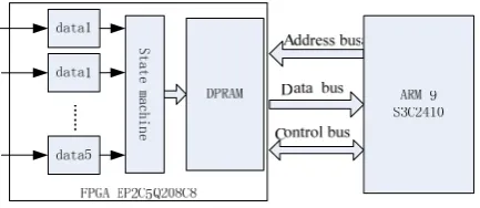
In the FPGA and ARM interactive system, 6 groups of synchronized parallel data were passed to ARM by FPGA in sequence, as shown in Figure 1. The hardware system used by FPGA is EP2C5Q208C8 of Cyclone II series of ALTERA Corporation. This type of chip is a kind of low-cost FPGA presented by 90nm technology based on Stratix II, with the high cost performance. The chip contains a variety of logical unites (nearly 5000 LE), 26 M4K RAM (4kbit), 2 PLL, 13 multiplier units, and 208
external lead feet. The CPU S3C2410 introduced by Samsung Corporation was chosen by ARM, which adopt ARM920T core, 0.13um COMS standard macro unit and memory unit. The basic frequency of the system is 400MHZ when working. The chip contains 64M NAND Flash and 64M SDRAM and a variety of sources. To the part of hardware system, it combines ARM and FPGA, taking advantage of the abundant logical sources inside FPGA and the parallelism hardware character, and makes use of the ideology of ping-pong controlling principle, deserializing and synchronization design to realize the function that the low speed module can process the high speed data. ARM takes FPGA as peripherals, which is external to the system bus on S3C2410 to achieve the data buffer. The ARM processor picks up the buffer data through reading on the external system bus FPGA.
Figure 1 Parallel data exchange system based ARM and FPGA III. METASTABILITY
A. Generation of metastability in Asynchronous Time Domain
The core of asynchronous clock domain transformation is to ensure the Setup/ Hold time of data sampling from the subordinate clock to the higher authority. If a trigger's Setup/ Hold time did not meet, it may appears metastability problem. Because in this case, the fan-out of trigger Q will be in limbo after a longer time of effective clock edge coming. During this time , fan-out of trigger Q may generate burr and constant oscillation , then finally fix in a ascertain voltage value. The voltage value does not necessarily equal to the data of original data input end D. This period is called Resolution time. After resolution time, the fan-out of trigger Q will stay at 0 or 1. It is random whether this is exactly 0 or 1 and it have no relationship with the input The paper is supported by the Education Department Project of
data[3], as shown in Figure 2.
aclk and bclk are the different clocks. When the data of output end Q0 drops from 1 to 0, the output signal aData may possibly be a burr , a shake or a voltage value before stabilizing down. At this time, the data gathered by clock
bclk
may probably be incorrect. It would causethe logical judging mistake or the spread of metastability state in some serious situations. The miscalculation of logic would lead to the functional error while the spread of metastable state would expand the failure surface. As
long as the system has an asynchronous clock domain data alternation, the metastable state is avoidless. Therefore, firstly, it should reduce the mistake when designing electric circuits. Secondly, you should make the system be insensitive to the errors. The realization of the former would rely on the synchronized design, and the latter must act to make the different designs according to different design applications, such as reducing the use of logic circuit and using the trigger which is not very sensitive to the burr[4].
bclk samples adapt while it is changing
Data changing Only one synchronizing flip-flop Data
aclk bclk
aData bData
Data aclk
bclk
aData
Q0 Q1
aclk is asynchronous
to bclk
Clocked signal is initially metastable …
… and might still be metastable at the next rising edge of bclk
Figure 2 Diagram of metastability generation
B. Solutions of the metastability problems
There are many solutions of metastability in asynchronous clock domain and the accustomed solutions are Gray coding, double trigger, asynchronous FIFO(first in first out) and DPRAM which is the most common solution[5].
(1) Double trigger method
Double trigger method, usually being understood as sampling the signal twice using trigger, means sampling anterior data twice using posterior clock. Figure 3 shows its working principle. Seeing from the diagram, the left is the input port and the right is output signal (bdat2) which will keep synchronous with bclk after sampling twice using trigger and will fundamentally not be in metastability. The explanation is that the Q port in first trigger may be in metastability state. But the probability
for unstable output level of D port in second trigger is very small after one Clk period. So the Q port in second trigger have little possibility to produce metastability. This solution can reduce transmission of the metastability state effectively, which make the latter circuit have stable electric level. However, Double trigger method can not guarantee the output level in the second trigger absolutely accurate. The reason is that once setup/hold time can not be ensured, the output level of trigger would not be a stable value after Resolution time. So this method can not get rid of the possibility to generate output error when exampling signal. But if the application is not rigor to sampling error of signal, applying it in circuit where the sampling clock has the same frequency but different phase is very appropriate.
(2) Asynchronous FIFO,DPRAM method
Use FIFO or DPRAM to solve metastability problems is undoubtedly the most reliable method, they can reduce the probability of metastable happen to very low. Writing asynchronous FIFO or DPRAM according to the timing is equivalent to put the data into the buffer and the data have enough time to stay stable, and thereby reducing the phenomenon that Metastable phenomenon happen because of the insufficient of Setup/Hold time . But the system still have to avoid reading and writing the same storage unit at the same time, for it will cause read-write conflicts, and this may lead to reading out a wrong value.
The ARM and FPGA communication will definitely involves the synchronous problems of data transmission in asynchronous clock domain and this is called metastability problems . This system uses asynchronous FIFO, DPRAM method for the reason that FPGA is internal integrated with free DPRAM IP core, and the IP modules inside the FPGA have passed strict tests and optimizations, so it can use the least logical resources to get the most optimal performance. Therefore, in the system, the simple DPRAM blocks with FPGA embedded has been selected as system data synchronizer. The internal structure of DPRAM has been shown in figure 4.
Figure 4 The internal structure of the DPRAM
In the figure, the realization of DPRAM module has use the macro unit of DPRAM as the main body ,which is integrated in Quarters II 9.0. the address bus width of DPRAM is 11 bits, the data bus width of DPRAM is 32 bits and the depth of DPRAM is 1440. DPRAM has independent read and write data bus, address bus and control bus, can implement an independent operation to any port.
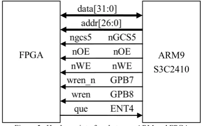
IV. ARM AND FPGA PARALLEL MODULE DESIGN In the hardware design of system, in order to enhance FPGA and ARM data transmission efficiency, we can hang FPGA on the ARM address bus as the memory and this results in the phenomenon that the ARM processor can visit the data of on-Chip RAM and register in the FPGA[6]directly .The hardware interface of FPGA
and ARM has been shown in Figure 5. FPGA data-bus
data, address-bus addr, chip select signal ngcs5 and
read-write enable signal n_OE, n_WEare connect to the ARM system bus correspondingly. FPGA start/strop signal , wren/wren_n are all connect with the ARM’s
I/O, which is used to realize the control of data interactive . Considering to avoid the signal disturbance phenomenon in the data transmission process , the start/strop signal is adopted in difference form. FPGA accepts the exterior data unceasingly, and save it in DPRAM. When data storage in the FPGA achieves the threshold value, FPGA sends interrupt request signal que to ARM, demand ARM to read the data. As soon as ARM receives interrupt request signal que from FPGA, it transfer an processing interrupt file and conduct the data reading operation.
In the system, when signal n_OE is effective, FPGA works as the data sending end, ARM works as the data receiving end. When signal n_WE is effective, FPGA works as the data receiving end, ARM works as the data sending end. When signal ngcs5 is ineffective, the data bus of FPGA must be at high-resistance situation, otherwise the whole system could not work.
FPGA ARM9 S3C2410 data[31:0]
nOE nGCS5
que
wren_n wren nOE ngcs5
GPB7 GPB8 ENT4
addr[26:0]
nWE nWE
Figure 5 Hardware interface between ARM and FPGA
A. FPGA output module.
In the FPGA interface module, FPGA must achieve to the function that can store six channel of synchronized parallel data into DPRAM accurately, according to certain order. FPGA output interface module has been shown in Figure 6 .
In the figure, the frequency of FPGA system clock clk is 20MHZ. We can achieve to write a data into an address repeatedly and thus reduce the ratio of data error by using clk_pll (100 MHZ) as the write clock of DPRAM .Write_req write the request signal for DPRAM, ngcs5 read the request signal for DPRAM and reset works as system reset signal. While wren =0, the system does not work, while wren=1, FPGA hardware system starts to work. FPGA write the Data data0-data5 which have been transferred from series connection to parallel connection into DPRAM in order under the distribution of RAM controller.
ARM accept the signal, it takes away the whole DPRAM data continuously.
In this system, the threshold value of DPRAM is 1440, since the transmission speed of each channel of data is 240kB/s and the six channels are synchronization parallel port; The time interval of data storage cycle of
DPRAM is larger than the time that ARM takes to read 1440 data. Therefore, the DPRAM read-write confliction could not occur.(Note: data0-data5 is called a cycle of data).
Figure 6 FPGA output interface module In the FPGA output module, the most core part is the
RAM controller, realized by a state machine. It not only need to write the data into RAM in different states according to the READ/WRITE timing of DPRAM, but also send a pulse interrupt request signal with appropriate width to ARM when achieving the threshold value. It is realized by a Moor state machine. The picture of state machine produced by Quartus II has been shown in Figure 7.
After six channels of data all arrive at data register data0-data5, the start signal of state machine flag has been set to1 spontaneously. Then the state machine start to work . If the state machine is in the state 0, the time delay several clock cycles, waiting for the data to keep stable and then open write enable signal of DPRAM. Then write the six channels of data into DPRAM in order.
Figure 7 Diagram of State machine
While under the state 7, close the write enable signal of DPRAM, and judge whether the data have reached the threshold value.Send out the signal of interrupt if it reaches the threshold value , then jumps to the state 0; Otherwise, jumps to the state 0 directly .At this time, the signal flag have already set to 0 automatically, the state machine stop working, waiting for the arrival of next cycle of data to strike the state machine to start to store the next cycle of data.
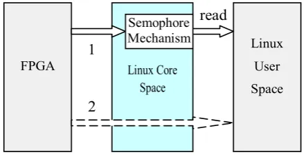
B. FPGA Drivers Design in Linux
In this system, the main function of FPGA drivers in Linux is to offer the user space connectors to read and write S_FIFO data. Through the design of commonly used drivers, FPGA data was written into Linux internal core space directly by suspend or DMA in the drivers. And realize the standard read and write function in the C storeroom for the users to use in the core driver module. This would lead to the data-copy twice. The way of the data transmission is shown in Fig.8.
FPGA
Linux User Space
2
read
Linux Core Space
1
Semophore Mechanism
definitely consume a mass of RAM. And if these RAM were not allowed to be swap-out, this will bring the system some bad effects to the function. In this system, the way of the data transmission is shown in figure 8.2. In the second type, the driver share the physical address of S_FIFO in FPGA directly to the consumer process space. In this way, the consumer process can read data directly from FPGA. The abuse of this means is that the consumer space can not use suspend and DMA and it can not meet the demand when the data transmission between ARM and FPGA have strictly timing sequence.
In this system, through tests, we find that when the synchro gorge of FPGA is under the condition of the highest data sampling rate, the speed that consumer process read S_FIFO is several times of the speed of S_FIFO overflow. So the driver uses the second type. In the period of the initialization of the driver, by calling alloc_chrdev_region to dynamic allocation a device number, calling cdev_init, cdev-add to register a driver module, then calling the core function like
devfs_mk_dir
、
devfs_mk_cdev、
devfs_mk_cdev tofabricate document root node of device. Through the calling of MMAP system of the driver, use remap_page_range to shine S_FIFO in FPGA to virtual space. And in this way, consumer process can use MMAP to get the virtual site of S_FIFO.
C. ARM to FPGA data reading.
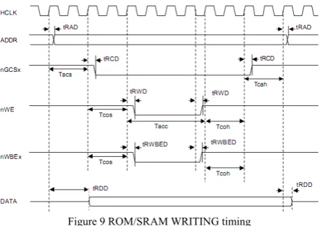
The DPRAM(DPRAM) , produced by using IP-core in quartus-ii in FPGA, is hanged up on the bank5 in memory address space of S3C2410. Its start address is 0x28000000 and the size is 64K Byte. When date communication is beginning between FPGA and ARM, the double port RAM in FPGA is read by ARM in the memory access method, so the access to DPRAM and access to ROM/SRAM have the same speed and some signal(such as DATA,ADDR and Ngcs5) are active at the same moment, Figure 9 shows the ROM/SRAM WRITING timing in S2410[7]. In this paper, some
parameters about READ timing shows as follow: Tacs = 0 Tcos = 0, Tacc = 14, Tcoh = 0, Tcah = 0, PMC = 0, ST = 0. The interface between FPGA and ARM use nGCS5& nOE as reading clock. When ARM read a data of one address in DPRAM, the level of nOE changes from high to low and the low level maintain 140ns(HCLK is 100MHZ), then the level of nOE changes from low to high and a reading operation is over.
When a group of data in DPRAM in FPGA is ready being read, the FPGA driver program in ARM(running Linux OS) will read data from DPRAM with interrupt mode and store them in distributed kernel space memory. After that, the sleeping application program in will be awaken by signal in kernel and complete the data copy from kernel space to user space.
Figure 9 ROM/SRAM WRITING timing
V. USING FLAG BIT SOLUTION DATA READ DISLOCATION PHENOMENON
ARM and FPGA parallel interface system require to keep stable and the data gathered should not have dislocation phenomenon. But actually,in the continual high speed data gathering process, the data dislocation occurs from time to time due to the disturbance of all kinds of factors. This would lead to the confusion of data when the data upload PC and display according to the sequence of channel. In order to avoid the appear of this kind of phenomenon and to be advantageous to follow the track to search the error and enable each group of data to integrate as a whole finally. The system takes some corresponding measurements. During the design of the system, we add some corresponding symbolic signal to each channel of signal or add a confirmation code to each cycle of storage during the process of storage as well as excellent coding style and the optimization of system design. As shown in Figure.10, the chart is aiming at raising a method for data smaller than 229.
D[31] D[30] D[29] … D[2] D[1] D[0]
n Data
The first channel flag flag0
The second channel flag flag1
The third channel flag flag2
The sixth channel flag flag5
the date ,in the DPRAM , DATA =DATAn+ flagn
0 0 0 0 0
0 0 1 0 0 0
0
0 1 0 0 0 0
…… ……
… …
0
1 0 1 …… 0 0 0
Figure 10 The design of dislocation flag module
Figure 11 Data after package dispatched
VI. CONCLUSION
In the ARM+FPGA hardware platform, this article designed the high speed parallel interface, that has been introduced above; Solved the data synchronization question of data transmission during the asynchronous time domain; Designed ARM and FPGA hardware interface module, the data output module ,FPGA driver
module and the data receive module; Introduced a method, it can prevent data dislocation phenomenon of high speed data transmission. In the system, the communication speed of data between ARM and FPGA can reach to 11.25Mbit/S, the test indicate that the system is stable, it proved ARM and FPGA high speed parallel interface accuracy and the reliability.
REFERENCES
[1] Yan, Lei; Zhao, Gang; Ryu, Si-Heon, G; Lee, Choon-Young; Lee, Sang-Ryong; Bae, Ki-Man. “The platform of image acquisition and processing system based on DSP and FPGA”[J]. ICSMA 2008 – International Conference on Smart Manufacturing Application 2008, p 470-473 [2] Yang, Shujie, Guo, Zonglian. “Development of high-speed
data acquisition system based on FPGA” [J]. Dianli Zidonghua Shebei / Electric Power Automation Equipment, v 28, n 6, June, 2008, p 93-96
[3] Fang Wei, Zhijun Liu, Kejie Ma. “Design and Realization of Asynchronous FIFO Based on Verilog HDL” [J]. Application of IntegrateCircuit.P97-100
[4] Jihua Wu, Cheng Wang. “Design of Altera FPGA/CPLD(
High Level Part)”. Publication of People Post and
Telecom . 2005.7
[5] Shiwei Xu,Yanyan Liu, Hongxia Liu. Asynchronous
Clock Metastable and FIFO Flag Bit [J]. Application Technology of Electronics. 2006.11. p99-101
[6] Yating Wang. High Speed Data Collect Technology Based on ARM and FPGA[D].University of Beijing Jiaotong. 2007
[7] SAMSUNG ELECTRONICS. S3C2410X 32-bit RISC microprocessor user’s manual.2003.
Daode Zhang Hubei Province,
China. Birthdate: August, 1973. Ph. D of Mechatronic Engineering from Huazhong University of Science and Technology. Research interests on embedded system, image recognition and intelligent control.
He is a associate professor of Dept. Machine engineering, Hubei University of Technology.
Yurong Pan HuBei Province,
China. Birthdate: January 1986. is a Mechanical design and automation Master’s degree, graduated from Dept. Mechanical engineering HuBei University of Technology. And research interests on image processing.
She is a student of Dept. Mechanical engineering HuBei University of Technology.
Xinyu Hu Hubei Province, China.
Birthdate: August, 1975. Mechatronic Engineering Doctor of Wuhan University of Technology, with research on image processing algorithm. Presided over 1 provincial scientific research projects and published more than 10 papers.