Simulation And Hardware Implementation Of
Pro-tection System For High Power Inverters Using
FPGA Controller
Ravindra Singh Rajput
Department of Electronics & Communication, Vario Infotech Pvt. Ltd, Noida, India. Email: [email protected]
ABSTRACT: This topic illuminates to develop the protectionsystem for high power inverters using FPGA (field programmable gate array) software. The current system consists of thyristor for the high power inverters and according to the simulation results hardware implementation is done with FPGA controller board. For the reference values for FPGA code generation, one power circuit can be developed with ZCD circuit, according to the result of the power circuit FPGA controller will work in such a way that if any fault occurs in the system then the system will be protected. FPGA board can be interface with the hardware and in software of FPGA program can be developed for the feedback of the protection system. However the system which can be developed in hardware or power circuit can be modify also with other power ratings and according to that FPGA controller will work and the system for the protection of the high power inverters can be easily implemented.
Keywords :Introduction of project, high power inverter, FPGA, Simulation Result, hardware etc.
1.
I
NTRODUCTIONBy designing the particular topology it is easy to obtain design simulation results and also by observing all the faults and all the parameters making close loop control system with the help of the microcontroller and the controller circuit with protection system of this high power inverter is implemented and then hardware system of this power module is implemented. Basi-cally in this system thyristor based circuit is being used and protection of that system is developed so during supply process as input voltage is given with that one IGBT swith is also being used to give opposite suplly to DC link to compen-sate harmonics and with using logical elements thyristor pulse is given so that we can get voltage across the thyristor and output voltage waveforms to develop protection system using FPGA within limit and snubber circuit and sharing resister are also to be added to the circuit for better output results
2. HIGH POWER INVERTERS.
Fig.1 Block Diagram Configuration
A. Proposed Topology
Basically in this high power inverter module, voltage level should be maintained so that other fault level can be de-creased. According to parallel load connection, inverter gate
drive circuits will change pulse for the thyrister. We can simu-late this inverter circuit in single phase and three phases also. In controller section FPGA is used so that perticuler limit for the peak value should be decided and according to that if fault goes above or below that limit the whole circuit will open so that components used in the circuit will be safe and protection of circuit can be easilly developed. Without use of snubber circuit, spikes in the voltage and distortion in the current wave-forms can clearly notify and that can be minimized only by adding snubber circuit. Sharing resister are also to be added in the circuit for the balancing of voltage levels. Voltage moni-toring and digital control system can be used also but FPGA is more user friendly than all other controller systems in recent days. Basically the model of the circuit consists of thyristor as a semiconductor devices and RL load. Gating pulse are ob-tained according to load changes and with the refrence of that particuler load, load voltage waveforms are being obtained which is given to the comparator and from that with using IGBT switch and logical elements pulses are given to the paires of thyristor accordingly via comparator. One thing is also to be noticed that main supply is given to the load side for the load voltage waveforms and another DC supply is given by the IGBT switch to the load side from the opposite side of main supply. The main reason of giving this supply is to eliminate harmonics and this IGBT switch is on for only 500us and after that this system doesn’t affect to the output voltage wave-forms. The pulses which are given to the thyristor have been given 0.2V DC source and being compared with the values of load side then output of the comparator is given to the thyristor gate pulses.The values of the load side, in which capacitor values are varies between 100uf and values of an inductor are varies between 65uH-80uH. The inductors which are being used for the filtering have values of 7uH. Waveforms across all the thyristor are obtained for the analysis and according to that parameters are decided for the FPGA controller.
B. Controller development
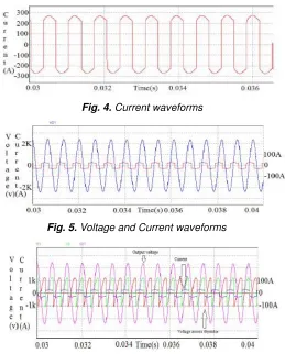
controller can manage the protection of the thyristor and other components so that the whole circuit will be safe within the limits. According to the pin diagram of FPGA controller, it is easy to enter the values of the different section for the varying output and it is also user friendly than the DSP which is being used for the controller. Programming and code generation in the FPGA is according to the fault level and other parameters which are being changed during fault according to the system. FPGA Cyclone controller consists of ADC, DAC, Buffer and some other ports are there for the analysis of the protection system for high power inverters. Here in Fig. 2 shows the vol-tage waveform across the thyristor and here in this system in single phase four thyristor are connected in one lag, it means two thyristors are in series in one lag so during positive half cycle four thyristor will conduct and negative half cycle other four thyristor will conduct in single phase system. Here the same voltage across thyristor waveforms we can get in hard-ware also which can be taken as a reference for the controller section. If we are using two thyristor are in series then the re-sults of that two thyristor will be almost same because thay are blocking same voltage but the voltage will get divide so as many thyristor used in a system we can say that the voltage will get balanced, so the load or stresses on each thyristor will get reduced. So according to the simulation and hardware results are being observed. By changing the parameters cur-rent and output voltage waveforms can also be varied. Here in Fig. 3 shows the output voltage waveforms of the system, bas-ically here output voltage waveform should be pure sinewave and it describe the system without any fault or losses. Basical-ly this output voltage waveforms are pure sinusoidal and which can be obtained by using LC filter also if harmonics or spikes are there. Here in Fig. 4 shows the current waveforms through the system and according to charging and discharging mode, positive and negative cycle, waveforms to be obtained.
3. SIMULATION RESULTS
Fig. 2. Voltage across thyristor
Fig. 3. Output voltage waveforms
Basically during operation periods, voltage across the thyristor which are shown in Fig.2 are due to inductive load so during positive half cycle, it slightly goes below zero due to inductive load and current which are shown in Fig.4 is depend on load which are connected. So according to the calculation of para-meter, voltage and current waveforms can be varied as load changes. Other thing is to be consider as a power factor ba-lancing, PF is maintained throughout the system nearer to uni-ty as much as possible to get desired values so here we are getting PF is around 0.95 which very much nearer to the unity and that shows the ratio of low losses in the system. PF should be in proper manner.
Fig. 4. Current waveforms
Fig. 5. Voltage and Current waveforms
Fig. 6. Voltage and Current waveforms.
4. HARDWARE DESCRIPTION
Here basically in hardware implement, one power circuit with ZCD is developed and the values with parameters like voltage across thyrisor, current in the system, reactance, impedance, capacitance etc should be measured and with taking the refer-ence values of these parameters, power circuit is being devel-oped.
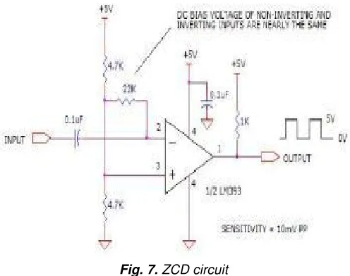
A. ZCD circuit
Reference values which can be generated by the analysis of power circuit can be modifying also by varying the values in power circuit as well as ZCD output analysis. The waveforms which we are getting in this power circuit in oscilloscope are similar to the simulation results, according to that limits in FPGA controller can be decided and programme for the close loop feedback is genera ed. And we can also say that this whole system can be implement in high rating also for the pro-tection of the system in some industry or somewhere. Pro-gramming in FPGA CONTROLLER is the heart of this imple-ment of the system because all the analysis of feedback and other parameters are depends on the controller section. Here in Hardware, ADC and DAC are used in controller section to get signal accordingly. They are designed to operate from sin-gle +5V supply with +10V multiplying referances for 4-quadrant output with 6.8 MHz bandwidth. The 4-4-quadrant re-sistors facilitate resistance matching and temperature tracking, which minimize the number of components needed for multi-quadrant applications. Hardware should be in such a way that simulation results which we have obtained are very much simi-lar to the hardware results.
Fig. 7. ZCD circuit
Here in Fig. 7 shows the ZCD circuit that can be used in a power circuit to get the result of the parameters so that it can be used as reference for the FPGA controller limit code gener-ation. The values we can see that LM393 is the regulator IC which can easily balance the voltage levels, capacitors with the values of 0.1uF are used with at least 5V rating. Resistors used here are 4.7K, 22K, 1K values. Basically output port of LM393 gives square wave signal as zero crossing detector circuit. Basically we want 5V output to give controller so from transformer we will supply to ZCD circuit and from ZCD we will get 5V detected output which will given to the controller sec-tion. Here in Fig. 8 it shows the block diagram of a power cir-cuit which is being used for the FPGA Controller reference.
B. Power circuit
ZCD produce narrow pulses to every zero crossing point, its pulses are applied to the port of a FPGA controller. The output of this is ANDed with astable output of 555 as a high frequency signal. And output of AND gate will be through amplifier & pulse transformer send to SCR gate.
Fig. 8. Power circuit block diagram
AD7671 plays an important role to ensure such parameters as signal-to-noise ratio (SNR) and total harmonic distortion (THD), in addition to the more traditional dc parameters of gain, offset, and linearity. It features a very high sampling rate mode, a fast mode for asynchronous conversion rate applica-tions, and for low power applicaapplica-tions, a reduced power mode (impulse) where the power is scaled with the throughput. In power circuit basically IC can be also varied by different topol-ogy varies because we want +5V output as ZCD accordingly, so by switch to other topology we can also get +5V output and according to the power circuit works.
5. FPGA CONTROLLER
FPGA controller is a field programmable gate array controller which works as DSP. Other useful parts are connected with the controller for the proper output.
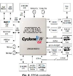
A. Block diagram analysis
Fig. 9. FPGA controller
Basically the board includes many components system troller which interfaces directly to the configuration, LCD con-trol, power monitoring control and other purposes. The system controller contains the required state machine and control logic to determine the configuration source for the controller. For the programming of the controller for one particular system, pro-gramming is possible through a serial flash loader and by per-forming in system programming through the AS programming header. Here FPGA configuration can be done by external USB-Blaster also. The processor of the FPGA can decom-presses the bit stream in real time and programs its SRAM cells.
B. Pin configuration analysis
The pin which is being used in the development for the protec-tion system is the CYCLONE FPGA 2C35. Generally all the components are being operated by this pin. Compressed and uncompressed configuration of data in same program file is possible. Basically compression can be done by enabling bit streams in convert program files. During the system power up, both cyclone FPGA and serial data configuration device enter into a power-on reset mode. The value of the pull-up resistors on I/0 pins can be varies according to the DC switching. The clock pulses which can be generated by the cyclone FPGA control the entire configuration of the protection system for the high power inverters. Basically this FPGA uses 10-MHZ inter-nal oscillator by default to initialize the different values of the parameters. Configuration of multiple devices in a cascading manner is also possible by using a single serial port. Here Fig.8 shows the pin diagram of FPGA controller in which flash, SDRAM, SRAM, 7-segment display, toggle switch, pushbutton switch, LED pins are there. In these system, interphase be-tween hardware components and FPGA controller is done and according to the fault occurs the controller gives feedback. Here basically limits are provided during code generation and programming in FPGA controller. It is easy to obtain hardware results after getting simulation results.
Fig. 10. Output Voltage Waveform Using FPGA Controller
(Scale X:axis:1 Div = 5.00ms, Y: axis: 1 Div = 5.00 V)
Thus the whole protection system can be implemented using simulation and FPGA controller for high power inverters and analysis and development can be done.
6. CONCLUSION
Here from this concept we can conclude that protection sys-tem for the high power inverters can be implemented by sens-ing the voltage across thyristor, snubber voltage and current waveforms in FPGA Controller and according to that result hardware system is also being implemented.
7. ACKNOWLEDGMENT
I wish to thanks Mr.Shamim Alam (Associate Professor), Mr. Vinod Kumar (HOD) and all Faculty member of electronic and communication department, Dronacharya Group of Institu-tion.A special note of thanks to Mr. Shamim Alam who insists me in the field of research. Now recently I am working in Vario infotech Pvt. Ltd. as an ‘Electronics Engineer’ I also thank to all my friends Susheel Singh (Software Engineer (CBS), Rahul Kumar Sharma (Electronics Engineer), Qasim Khan (Produc-tion Engineer) & all Vario members for better support.
8. REFERENCES
[1] International Journal of Emerging Science and Engineer-ing (IJESE) ISSN: 2319–6378, Volume-1, Issue-5, March 2013. Design of Snubber Circuit for Thyristors Using Pspice by Nancy Merin Thomas.
[2] T. M. Undeland, F. Jenset, A. Steinbakk, T. Rogne, and M. Hemes, “A snubber configuration for both power transis-tors and GTO PWM inverters,” in Con$ Rec. 1984 IEEE Power Electron. Specialist Con$(PESC), pp. 42-53.
[3] I. Khan, J. Tapson and I. De Vries, “Automatic Frequency Control of an Induction Furnace”, Proc. IEEE Con$, A@icon ’99, v01.2, September 1999, pp. 913-916.
[4] J. M. Ho and F. C. Juang, “4 Practical PWM Inverter Con-trol Circuitry for Induction Heating and Studying of the Performance under Load Variations”, Proc. IEEE Con$ International Symposium on Industrial Electronics, vol. 1, July 1998, pp. 294-299.
Distributed Power Generation Systems,” IEEE Trans. Ind. Electron., Vol. 53, pp. 1398-1408, Oct.2006.
[6] J. Satry, O. Ojo, and Z. Wu, “High-performance control of boost ACDC PWM rectifier/induction generator system,” IEEE Trans. Ind. Appl., vol. 42, no. 5, pp1146-1154, Sept./Oct., 2006.
[7] Nancy Merin Thomas “International Journal of Emerging Science and Engineering (IJESE)” ISSN: 2319–6378, Vo-lume-1, Issue-5, and March 2013. [8] A Large-Capacity GTO Inverter with Low-Loss Snubber Circuits. N. Kawa-kami, S. Ueda, Member, IEEE, M. Hombu, Senior Mem-ber, IEEE, A. Ueda, MemMem-ber, IEEE, and Y. Jifuku. IEEE TRANSACTIONS ON INDUSTRY APPLICATIONS, VOL. 29, NO. 6, NOVEMBER/DECEMBER 1993. Short-circuit protection for three phase power inverters, International IOR rectifier, the power management leader.
[10] Design of snubber circuit of thyristor using Pspice, Inter-national Journal of Emerging Science and Engineering (IJESE) ISSN: 2319–6378, Volume-1, Issue-5, March 2013.