http://www.sciencepublishinggroup.com/j/ajop doi: 10.11648/j.ajop.20190702.11
ISSN: 2330-8486 (Print); ISSN: 2330-8494 (Online)
Letter
Optoelectronic Module with Integrated Transceiver and
Mux-Demux for Optical Interconnect Applications
Nga Thi Hang Nguyen
1, Ikechi Augustine Ukaegbu
2, *, Jamshid Sangirov
1, Hyo-Hoon Park
11
Electrical Engineering Department, Korea Advanced Institute of Science and Technology (KAIST), Deajeon, South Korea
2
Electrical and Computer Engineering Department, Nazarbayev University (NU), Nur-Sultan, Kazakhstan
Email address:
*Corresponding author
To cite this article:
Nga Thi Hang Nguyen, Ikechi Augustine Ukaegbu, Jamshid Sangirov, Hyo-Hoon Park. Optoelectronic Module with Integrated Transceiver and Mux-Demux for Optical Interconnect Applications. American Journal of Optics and Photonics. Vol. 7, No. 2, 2019, pp. 28-32. doi: 10.11648/j.ajop.20190702.11
Received: June 21, 2019; Accepted: July 12, 2019; Published: July 24, 2019
Abstract:
The design, development and improvtableement in electronic devices and components have led to the further miniaturization of the system devices and their interconnecting interfaces. Hence, reducing the size of the transmitter (Tx) chips, receiver (Rx) chips and associated components play an important role in designing a reduced/small sized optoelectronic modules for optical interconnect applications. Some of the associated components include multiplexer, demultiplexer, clock and data recovery circuits (CDR), etc. Therefore, in this paper we present an optoelectronic module with integrated transceiver (Tx-Rx) and multiplexer-demultiplexer (mux-demux) with the aim of reducing the total area occupied by the chips. The topology is based on sharing common blocks between Tx and Rx as well as Mux and Demux for saving chip area, power consumption and board area. Based on this topology, a design of 2-channel Tx/Mux and Rx/Demux is realized in a 0.18 µm CMOS technology. Themeasurement results show clear output eye diagrams at 2.5 Gbps with the voltage swing of 375 mVpp from the Rx/Demux. The
combined solution would save the chip area and power consumption of 10% and 23%, respectively, compared to discrete circuits implementations. Using this topology, a high efficient bidirectional optical link could be implemented in modern computer and other green IT applications.
Keywords:
Multiplexer, Demultiplexer, Bidirectional, Transceiver, Integrated Optoelectronics1. Introduction
System clock speed is rapidly increasing and the copper-based links on printed circuit boards (PCBs) constitute the bottle-neck of the high speed signal transmission between CPU and memory in modern computer systems. This is due to issues such as signal integrity, crosstalk, power consumption and electromagnetic interference. Optical links have been considered as one of the most promising candidates for replacing the electrical links [1-2]. Traditionally, optical links consist of a transmitter at the transmitting end and a receiver at the receiving end. A transmitter (Tx) module consists of a Tx chip and a Vertical Cavity Surface Emitting Laser (VCSEL) for transmitting and a receiver module (Rx) consists of an Rx
chip and a photodiode (PD) for receiving.
Sangirov et al and Ngo et al [6-7]. Operations of up to 2.5 Gbps was achieved in Kang’s work [4] and 7 Gbps in Ukaegbu’s work [5], respectively.
In conventional Tx-Rx topology, which in many cases have several data lines for exchanging data between CPU and memory, the cost of power, chip area and board area for sending and receiving data when every electrical line is replaced by each optical line is large. However, several solutions have been demonstrated and implemented. In the works by Nguyen et al and Sangirov et al [8-10], a single fiber was used to send and receive data simultaneously (in full duplex mode), where the Tx and Rx chips have been implemented on separate chips. For communication between CPU and memory, separate I/O pins would be required when using implementations of the works by Nguyen et al and Sangirov et al [8-10] and hence requiring a single pin for transmit and a single pin for receive. Half duplex operation was achieved in Kang’s work [4] while both full and half duplex operation were achieved in Ukaegbu’s work [4]. In Kang’s and Ukaegbu’s works [4-5], both the Tx and Rx are implemented on a single chip with a shared gain stage (limiting amplifier stage). However, in Ukaegbu’s work [5] a single pin is used for both transmit and receive. In order to increase throughput while transmitting data of the same type, multiple transmit pins and multiple receive pins need to be used over a single transmission line. To solve this problem, a multiplexer (Mux) and a demultiplexer (Demux) can be used to convert the slow speed parallel data to a serialized high speed data in the transmitting side and vice versa in the receiving side to replace many electrical data line using a single optical link. Several works have been reported on Mux and Demux designs by Chien et al, Luo et al, Sekiguchi et al, Rubiya et al, and Meghelli et al [11-15]. However, most of them are usually discrete implementations of Mux and Demux. Also, designs with the Mux, Tx, Rx, Demux are usually implemented on discrete chips thus, resulting to large chip area, more power consumption, while occupying larger board area. On the other hand, the wire bonding between these discrete chips leads to increased noise and this is undesirable for an optical link system. Moreover, discrete chips result to complicated DC/AC matching between the chips.
In this paper, an optoelectronic module with integrated Tx-Rx and Mux-Demux topology is proposed to multiplex/demultiplex multi electrical lines to/from a single optical signal line. With this topology, an optical link comprises of Mux, Tx, and VCSEL for the transmitting mode and PD, Rx, and Demux for the receiving mode, where the combined Mux-Demux and Tx-Rx are integrated on a single chip. Additionally, the combined Mux-Demux as well as Tx-Rx can share common blocks to further save chip area and power consumption. In our proposed topology, Mux-Tx and Rx-Demux chips are realized in a 0.18 µm TSMC CMOS technology. The chip design as well as the measurement results and chip photographs for integrating 2:1 Mux-Tx and 1:2 Demux-Rx chips are presented.
2. The Proposed Optoelectronic Module
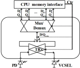
In our proposed topology, the TRx (Tx-Rx) can share a common space on a single chip. The share of the common block of two circuits makes it possible to save 55% or 20% of power dissipation, depending on the operating mode. The chip is fabricated in a 0.18 µm CMOS technology and occupies an area of 0.82 × 0.82 mm2, which is about 70% of the total area of a typical unshared Tx-Rx chip. This chip can be applied for point-to-point and parallel multi point optical links. In order to have a large bandwidth, where a single optical link can replace multiple electrical links, an optoelectronic module with integrated Tx-Rx and Mux-Demux is proposed. The proposed topology is shown in Figure 1.
Figure 1. The proposed Optoelectronic module with integrated Tx-Rx (TRx) and Mux-Demux.
The topology is special for replacing multi parallel time interleaving electrical links using a single optical link. The integration and combination have merits such as chip size and power consumption of chips for optical link system. On the other hand, the integration allows for a more reliable system as there is no need to interface between discrete chips using wire bonds. Additionally, many parallel electrical lines will be replaced by one optical line. The number of optical devices (VCSEL and PD), the space occupied on the board, as well as the complexity of the system will be reduced.
The Mux/Tx and Rx/Demux functions of this chip are controlled by switches (SWs) according to the status of control signal (Ctr). A high Ctr signal allows the chip to work in the Tx/Mux mode. The Mux, which works as a serializer, converts the parallel input data (D0~Dn) to a high-speed serial
data (Dout) which is then amplified by gain stage and
modulated by VCSEL for transmission. A low Ctr signal will make the chip to operate in the Rx/Demux mode. The optical signal is converted by PD to a current signal. This small and noisy current signal then is amplified and reshaped by trans-impedance amplifier (TIA) and limiting amplifier (LA). Finally, the Demux converts this serial electrical data to parallel output data (Q0~Qn).
3. Circuit Design and Implementation
introduced in this section.
3.1. Mux/Tx Design
3.1.1. 2:1 Mux Cell Design
Figure 2(a) is the schematic of a 2:1 Mux cell, consisting of five latches L1-L5 to avoid the simultaneous transition in both
inputs of the selector (SEL) and a SEL for serializing input data. The inductorless CML circuit is used in designing the latches and selector for high speed operation. The latches and selector work based on the clock signal (Clk). When the Clk is high, the L1, L3 and L4 are obscure and the SEL selects the
output of M3 while L2 senses the output of L1 and L5 sense the
output of L4. When the Clk is low, the output of L2 will be
sensed whereas L5 becomes obscure providing a stable level
for the SEL.The 2 inputs are turn by turn selected to the output (serialized) based on the Clk.
(a)
(b)
Figure 2. (a) 2:1 Mux cell block diagram and schematics and (b) Tx block
diagram and schematics.
3.1.2. The Tx Design
Figure 2(b) shows the block diagram and schematics of Tx. The Tx is made up of a gain stage and a driver stage. In the gain stage, three differential gain pairs (M1, M2; M5 M6; M7 M8)
are used for high gain and large bandwidth. The M3, M4 pair
forms an active feedback; M11, R1 and M12, R2 pairs work as
active inductors. The M9,M10 pair with C forms an active
capacitor to enhance the bandwidth of the gain stage. The driver consists of two differential pairs for driving large current to the output and a source follower buffer for impedance matching to VCSEL. Figure 3 shows the frequency response of the Tx. A 3-dB bandwidth of 4.2 GHz with a gain of 39dB were achieved.
Figure 3. Frequency response of the Tx.
(a)
(b)
3.2. Rx/Demux Design
3.2.1. 1:2 Demux Cell Design
Figure 4 (a) shows the 1:2 Demux cell schematic. The cell uses both rising and falling Clk edges and operates at half the clock speed of the input data rate Din. During high interval of
the Clk, the L3 trace the first bit of Din. When the Clk
transitions from high to low, the stored bit at the input of L3 is
locked and L4 will capture the signal from L3 at the falling
edge of the Clk. During the low interval of Clk, the first bit of Din is transferred to output2 (Q2) while L1 traces the second bit
of Din. When the Clk transitions from low to high, the second
stored bit at the input of L1 is locked and L2 captures the signal
from L1 at the rising edge of the clock. During the high Clk
interval, the second bit of Din will be transferred to the ouput1
(Q1). This process will deserialize the Din to two parallel
outputs.
3.2.2. The Rx Design
The Rx consists of a TIA, a gain stage limiting amplifier (LA) and an output buffer. Figure 4(b) presents the block diagram and schematics of the proposed optical receiver where two identical TIAs are used for differential signal, one of them is a dummy with the same input capacitance as the photodiode capacitance.
The TIA is implemented using advanced CG topology for isolating the large input parasitic capacitance from the bandwidth degradation, according to Kang et al [4]. On the other hand, an NMOS active inductor and a resistor are used to strengthen the bandwidth.
The number of gain stages of LA have been considered for optimising the trade-off between gain, input-referred noise, power consumption and bandwidth. In Figure 4(b), a gain stage cell of LA is presented. A negative active feedback through differential transistor pair (M3, M4) and an active
inductor load for the second stage of the gain cell are used to enhance the bandwidth. Additionally, a negative capacitance is used to reduce the high impedance between the cascading amplifiers as well as a slew-rate boosting to remove the low-setting of the output waveform through M9, M10,and the
capacitance, C. Figure 5 shows the frequency response of the Rx. A 3-dB bandwidth of 4.3 GHz with a gain of 81dB were achieved.
Figure 5. Frequency response of the Rx.
4. Experimental Results
The optoelectronic module with integrated transceiver (Tx-Rx) and a Mux-Demux. The module was designed with the Mux/Tx on one side and the Rx/Demux on another side. They were designed and fabricated in a 0.18µm TSMC CMOS technology. For demonstration purposes, the chips were fabricated and measured separately (i.e. the Tx/Mux as a separate chip and the Rx/Demux as a separate chip). The chip photographs of Tx/Mux and Rx/Demux are presented in Figures 6(a) and (b) respectively. The layouts of digital part Mux-Demux and of analog part Tx-Rx are carefully isolated to minimize the noise from digital part interfering to analog signal. The chip area of the Tx/Mux and Rx/Demux are
540x1320 µm2 and 594x1089 µm2 (including pads),
respectively. For measurement purposes, Teflon based evaluation boards were used. The chips were packaged on the evaluation board by die-bonding the chips on the boards and wire-bonding them where necessary. Figure 7 shows a photograph of the packaged chips. A power consumptions of 112 mA and 122 mA were achieved for the Tx/Mux and Rx/Demux, respectively, under a 1.8 V power supply. The total chip area and power consumption reduction of 10% and 23%, respectively, were achieved when compared to discrete chips.
(a)
(b)
Figure 6. The chip photographs of the (a) Tx/Mux and (b) Rx/Demux.
Figure 7. The photograph of evaluation board with packaged chips.
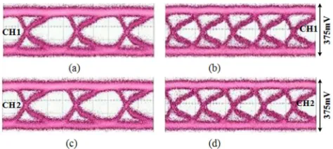
Figure 8. Measurement results of 2 channels of the Rx/Demux where (a), (c) are the eye measurements at 3 Gbps for channels 1 and 2, respectively and (b), (d) are the eye measurements at 5 Gbps for channels 1 and 2, respectively.
5. Conclusion
In this paper, an optoelectronic module with integrated transceiver (Tx-Rx) and Mux-Demux for optical interconnect applications have been proposed and implemented. A combined 2:1 Mux/Tx for transmitting mode and combined Rx/1:2 Demux for receiving mode have been presented. Designed in a 0.18 µm CMOS technology, the chips work well up to 5 Gbps. Open and clear eye diagram output signal with the voltage swing on 50 Ω impedance of 375 mV were achieved. The combined solution would save the chip area and power consumption of 10% and 23%, respectively, compared to discrete circuits implementations. The optoelectronic module has applications for serializing and deserializing the multiple point-to-point links between CPU and memory using a single optical link. The module could be applied for optical interconnects as well as other green IT applications.
References
[1] M. Forbes, "Optically interconnected electronic chips: a tutorial and review of the technology," Electronics & Communication Engineering Journal, vol. 13, no. 5, pp. 221– 232, Oct. 2001.
[2] H. S. Cho, S. Kang, M. H. Cho, B. S. Rho, H.-H. Park, K. U. Shin, S.-W. Ha, B.-H. Rhee, D.-S. Kim, S. T. Jung, T. Kim, “On-board optical interconnection of 2.5 Gb/s x 12 channels data using fiber-embedded PCB,” Proc. of IEEE/ICACT2004,
Phoenix Park, Korea, pp. 286-290.
[3] W. S Oh, K. Park, J. C. Choi, C. J. Kim, S. I. Lee and J. K. Moon, “Design of a 12 channel 120 Gb/s Optical Receiver Array in 0.18 µm CMOS Technology’, Electronic Design, Test and Applications (DELTA 2008), 4th IEEE International Symposium 23-25 Jan. 2008, pp. 71-74
[4] S.-K. Kang, T.-W. Lee, S. H. Hwang, M. H. Cho, H.-H. Park, “Demonstration of bidirectional optical link on optical PCB using a driver-receiver combined CMOS transceiver,” Proc. of 56th Electron. Comp. and Technol. pp. 1578-1582, 2006.
[5] I. A. Ukaegbu, M. Rakib-Uddin, J. Sangirov, N. T. H. Nguyen, T.-W. Lee, M.-H. Cho, H.-H. Park “Design of Full-duplex and Multifunction Bidirectional CMOS Transceiver for Optical Interconnect Applications” Optical and Quantum Electronics, vol. 49, no. 7, pp. 243, July, 2017.
[6] J. Sangirov, I. A. Ukaegbu, G. Sangirov, T.-W. Lee, H.-H. Park, “Power-aware transceiver design for half-duplex bidirectional chip-to-chip optical interconnects,” Journal of Semiconductors, vol. 34, no. 12, pp. 125001, December, 2013.
[7] T.-H. Ngo, N. T. H. Nguyen, I. A. Ukaegbu, T.-W. Lee, H.-H. Park “Bidirectional CMOS Transceiver with Automatic Mode Control for Chip-to-chip Optical Interconnects,” IEEE Photonics Technology Letters, vol. 21, no. 20, pp. 1241-1243, 2009.
[8] N. T. H. Nguyen, I. A. Ukaegbu, J. Sangirov, M.-H. Cho, T.-W. Lee, H.-H. Park, “Biwavelength transceiver module for parallel simultaneous bidirectional optical interconnections,” Optical Engineering Letters, vol. 52, no. 12, pp. 120502-120502, December, 2013.
[9] J. Sangirov, G.-C. Joo, J.-S. Choi, D.-H. Kim, B.-S. Yoo, I. A. Ukaegbu, N. T. H. Nga, J.-H. Kim, T.-W. Lee, M. H. Cho, H.-H. Park, “40 Gb/s optical subassembly module for a multi-channel bidirectional optical link”, Optics Express, vol. 22, no.2, pp. 1768-1783, January, 2014.
[10] N. T. H. Nguyen, J. Sangirov, G.-C. Joo, B.-S. Yoo, I. A. Ukaegbu, T.-W. Lee, M.-H. Cho, H.-H. Park “10 Gbps/ch Full-Duplex Optical Link Using a Single-fiber Channel for Signal Transmission” IEEE Photonics Technology Letters, vol. 26, no. 6, pp. 609-612, January, 2014.
[11] J.-C. Chien, L.-H. Lu, “A 15-Gb/s 2:1 multiplexer in 0.18-µm CMOS,” IEEE Microwave and Wireless Components Letters, vol. 16, no. 10, October 2006.
[12] Y. Luo, G. Chen, K. Zhou, “60 Gb/s low jitter 4:1 Mux and 1:4 Demux,” IEEE Midwest Symposium on Circuits and Systems, pp. 590-593, September 2008.
[13] T. Sekiguchi, S. Amakawa, N. Ishihara, K. Masu, “Inductorless 8.9 mW 25 Gb/s 1:4 Demux and 4 mW 13 Gb/s 4:1 Mux in 90 nm CMOS,” Journal of Semiconductor Technology and Science, vol. 10, no. 3, Sept. 2010.
[14] G. Rubiya, S. Vyshnavi, “ Transformer-coupled (TC) technique for the 2:1 Mux and the 1:2 Demux toserialize-and-deserialize (Serdes) high speed data sequence, “ International Journal of Innovative Research in Science, Engineering and Technology, vol. 6, no. 9, Sept. 2017.