Design and Optimization of an Efficient (96.1%) and
Compact (2 kW/dm
3
) Bidirectional Isolated
Single-Phase Dual Active Bridge Ac–Dc Converter
Jordi Everts
Department of Electrical Engineering, Electromechanics and Power Electronics (EPE) group, Eindhoven University of Technology (TU/e), 5600 MB Eindhoven (Postbox 513), The Netherlands; [email protected]
Abstract: The growing attention for plug-in electric vehicles, and the associated high-performance demands, have initiated a development trend towards highly efficient and compact on-board battery chargers. These isolated ac–dc converters are most commonly realized using two conversion stages, combining a non-isolated power factor correction (PFC) rectifier with an isolated dc–dc converter. This, however, involves two loss stages and a relatively high component count, limiting the achievable efficiency and power density and resulting in high costs. In this paper a single-stage converter approach is analyzed to realize a single-phase ac–dc converter, combining all functionalities into one conversion stage and thus enabling a cost-effective efficiency and power density increase. The converter topology consists of a quasi-lossless synchronous rectifier followed by an isolated dual active bridge (DAB) dc–dc converter, putting a small filter capacitor in between. To show the performance potential of this bidirectional, isolated ac–dc converter, a comprehensive design procedure and multi-objective optimization with respect to efficiency and power density is presented, using detailed loss and volume models. The models and procedures are verified by a 3.7 kW hardware demonstrator, interfacing a 400 V dc-bus with the single-phase 230 V, 50 Hz utility grid. Measurement results indicate a state-of-the-art efficiency of 96.1% and power density of 2 kW/dm3, confirming the competitiveness of the investigated single-stage DAB ac–dc converter.
Keywords: ac–dc power converters; battery chargers; dual active bridge; DAB; optimal design; power MOSFETs; single-stage
1. Introduction
1.1. Overview and Objectives
Single-phase utility-interfaced ac–dc converters with power factor correction (PFC) and galvanic isolation cover a wide range of applications such as chargers for plug-in hybrid electrical vehicles (PHEVs) and battery electric vehicles (BEVs) [1,2], interfaces for residential dc distribution systems and energy storage systems [3,4], and inverters for photovoltaic modules. Bidirectional power flow is increasingly required since the traditional electricity grid is evolving towards a smart interactive service network (customers/operators) in which energy systems play an active role in providing different types of support to the grid [5], e.g. vehicle-to-grid (V2G) concepts [6].
Figure 1.Schematic of the single-stage (1-S), single-phase, bidirectional, isolated DAB ac–dc converter topology. The nominal ac input voltage, input current, and power are respectively 230 Vrms, 16 Arms,
and 3.7 kW, while the specified output voltage range isVdc,2=370−470 V, withVdc,2,nom=400 V.
resonant topologies, whether or not combined with active auxiliary snubber circuits and/or a second, typically hard-switched and non-isolated, dc–dc conversion stage.
Besides the 2-S approach, several single-stage (1-S), single-phase, isolated ac–dc PFC converter topologies have been proposed in literature, which combine all functionalities into one conversion stage and thus (potentially) enable a cost-effective efficiency and power density increase through the omission of a complete loss stage and through reduction of the component count. Moreover, due to the absence of an intermediate dc-link there is no need anymore for bulky, failure-prone electrolytic capacitors. This, however, is at the expense of an increased filtering effort at the dc output side due to the double line-frequency (i.e. 100 Hz) power pulsation that is seen by the output, where large low-frequency (LF) filter capacitors are required in case a low output voltage ripple is desired. An example of a 1-S, single-phase, bidirectional, isolated ac–dc converter is presented in [19,20], using a cyclo-converter at the primary side and a voltage source converter at the secondary side of a medium frequency transformer. Another well known example is the 1-S DAB ac–dc converter topology analyzed in [21–27], which is able to effectively obtain PFC while producing high-quality waveforms and complying to regulations on low- and high-frequency distortions of the mains ac power lines. The topology is shown in Figure1 and is the subject of this paper. It consists of a quasi-lossless synchronous rectifier (SR) and an isolated full-bridge full-bridge DAB dc–dc converter, putting a small HF filter capacitor in between. Moreover, using advanced modulation schemes such as the one recently presented in [25], the DAB can be operated with minimum HF circulating currents and under full-operating-range zero voltage switching (ZVS) conditions, quasi completely eliminating the losses associated with the switching of the, in the case of this paper, MOSFET-type power switches.
Table 1.Operating Conditions and Converter Specifications
Property Value
ac-side
Vac(Vrms) 230 (nominal)
2076Vac6253
Iac,nom(Arms) 16 (nominal)
fL(Hz) 50
dc-side Vdc,2(V) 3706Vdc,26470 EMC compliance CISPR 22 Class B
PF >0.9 (atIac>0.1·Iac,nom)
THD IEC 61000-3-2 standard, and THD65% (atIac>0.3·Iac,nom)
Additional requirements
• Galvanic isolation
• Bidirectional power flow capability • High conversion efficiency (η>94%
within reasonable power range) • High power density (ρ>2 kW/liter) • Autonomous air cooling
• MOSFET-type power switches
a very high conversion efficiency and power density, high power factor (PF), and low total harmonic distortion (THD) of the ac input current while complying to the CISPR 22 Class B standard for EMC.
1.2. Outline
At first, in Section2 the general operating principle of the 1-S DAB ac–dc converter and the operating conditions of the DAB dc–dc converter, as core building block, are presented. Next, in Section3the operating principle, available modulation parameters, and relevant switching modes of the DAB are detailed and the method used for calculating an efficient full-operating-range ZVS modulation scheme is summarized. The selection of the high-level circuit variables such as the switching frequency, the inductance values, and the transformer’s turns ratio is outlined as well. Based on the available degrees of freedom in the design of the 1-S DAB ac–dc converter, in Section4the modeling of the losses and volumes of the employed components is discussed and the corresponding optimization results are presented. Subsequently, in Section5the designed hardware demonstrator is shown and its performance, i.e. in terms of losses (& efficiency) and volume (& power density), is calculated. In order to verify the optimization results, different measurement results are presented in Section6. Finally, conclusions are drawn in Section7.
2. General Operating Principle of the 1-S DAB Ac–Dc Converter
The investigated single-stage (1-S), single-phase ac–dc converter topology shown in Figure 1 consists of a synchronous rectifier (SR) and isolated full-bridge full-bridge dual active bridge (DAB) dc–dc converter as the core building block, putting a small high-frequency (HF) filter capacitorC1in between. Also shown in Figure1are the principle current and voltage waveforms at the different converter ports. The SR switches at each zero-crossing of the ac line voltagevac, folding it into a dc voltagevdc,1that varies according to the absolute value ofvac, i.e. at twice the 50 Hz line frequency (2· fL), and that is directly fed to the input of the DAB dc–dc converter:
vdc,1=|vac|=
Vˆacsin(ωLt)
, (1)
where ˆVacis the amplitude ofvacandωL = 2πfL. The DAB performs the PFC by actively shaping the switching-cycle averaged valuehidc,1iof its input currentidc,1in phase withvdc,1:
hidc,1i=dir·
Iˆac∗ ·sin(ωLt)
, (2)
where ˆIac∗ (= √
2Iac∗)is the amplitude set-point of ac input currentiacanddirthe power flow direction in accordance to Figure1:
dir= (
1 ifP>0 : prim. side→sec. side,
flow are identical.
0 2 5. 5 7.5 10
0
−10 10 20 30 40
−100 100 200 300 400
0
Figure 2. Ideal ac input-side quantitiesvdc,1,iac, andhidc,1iwithin a 10 ms half period of the grid
voltagevacforIac=Iac,nom=16 Arms(100% power) andIac=0.2·Iac,nom=3.2 Arms(20% power).
3. Optimal Zero Voltage Switching (ZVS) Operation of the DAB Dc–Dc converter
3.1. Operating Principle, Available Modulation Parameters, and Relevant Switching Modes
Control of the switching-cycle averaged DAB input currenthidc,1iaccording to (2) can be done by proper modulation of the full bridges (S11...14andS21...24) of the DAB dc–dc converter [] (see Figure1). Thereby, the bridges produce phase-shifted edge-resonant square wave voltages v1 and v2 at the terminals of a HF ac-link. This link consists of a HF transformer (ratio N = n1/n2) and external series inductor Lext. Also included in the ac-link are, so called, commutation inductances L1 and L2 which ‘inject’ relatively small, purely reactive currents into the bridges of the DAB, enhancing the commutation of the bridge legs without contributing to the power flow. In [25] and [26] they have been shown to be essential elements for achieving full-operating-range ZVS of the DAB with smooth modulation parameter trajectories. On the assumption of ideal components, the DAB can be represented by the primary-side referred equivalent model shown in Figure3, where the main energy transfer inductanceLconsists of external inductanceLextcombined with the leakage inductancesLσ1 andLσ2(not shown in Figure1) of the transformer:
L= Lext+Lσ1+N2·Lσ2. (4)
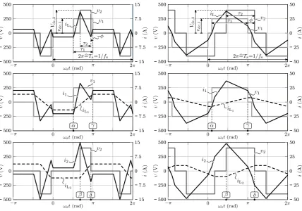
Figure4, which depicts general waveforms ofv1andv2for the two most appropriate switching modes, i.e. low-power mode 1 and high-power mode 2, for positive power flow of the DAB, defines the parameters available to modulate these voltages, being the phase-shift angleφbetweenv1and v2, the respective pulse-width modulation anglesτ1andτ2, and the switching frequencyfs. As in the following it is assumed that the switching frequency value/pattern is predefined (see Section3.3),
1 Note that around the zero crossing (−30 V6v
ac630 V) the bridges of the DAB are inactive (‘dead zone’) as zero voltage
Figure 3.Simplified (lossless), primary-side referred equivalent model of the DAB dc–dc converter. −15 −7.5 0 7.5 15 −500 −250 0 250 500 −500 −250 0 250 500 −15 −7.5 0 7.5 15 −500 −250 0 250 500 −15 −7.5 0 7.5 15
(a) Switching mode 1; low input current/power intervals. −500 −250 0 250 500 −50 −25 0 25 50 −50 −25 0 25 50 −500 −250 0 250 500 −50 −25 0 25 50 −500 −250 0 250 500
(b) Switching mode 2; high input current/power intervals.
Figure 4.Ideal HF ac-link voltage/current waveforms for (a) mode 1 and (b) mode 2, being derived using:vdc,1=250 V,Vdc,2=400 V, andfs=120 kHz. For mode 1 the selected modulation parameters
are:τ1 =1.53 rad.,τ2 =0.85 rad.,φ=−0.16 rad., resulting inhidc,1i=2 A. For mode 2 the selected
modulation parameters are:τ1=2.83 rad.,τ2=2.24 rad.,φ=0.54 rad., resulting inhidc,1i=22 A.
this results in a total of three ‘free’ modulation parameters: x = {φ,τ1,τ2}. The respective inductor currents, induced by voltagesv1andv2, are also shown in Figure4, whereby:
diL(t) dt =
v1(t)−N v2(t)
L , (5)
diL1(t)
dt = v1(t)
L1 , (6)
diL2(t)
dt = v2(t)
L2 . (7) iL1 andiL2, induced in commutation inductancesL1andL2, are the purely reactive currents that are
‘injected’ into the bridges of the DAB. As a result, the bridge currentsi1andi2are calculated as:
i1=iL+iL1, (8) i2=N iL−iL2. (9)
(a) (b)
Figure 5. (a) Characteristic of the non-linear parasitic output capacitance of the used FAIRCHILD FCH76N60NF MOSFETs. (b) Charge required to charge/discharge the MOSFET’s non-linear parasitic output capacitanceCossfrom 0 V toVdc(or vice versa) during commutation of a bridge leg.
hidc,1i= 1 Ts
Z (k+1)Ts kTs
idc,1(t)dt. (10)
Equations forhidc,1i, regarding the two switching modes of Figure4, can be found in [25]. 3.2. Efficient ZVS Modulation Scheme
The method used to calculate an efficient, full-operating-range ZVS modulation scheme for the DAB is presented in [25]. It is based on a constrained numerical optimization algorithm that calculated the modulation parametersx={φ,τ1,τ2}in each DAB operating point {hidc,1i,vdc,1,Vdc,2} based on a given switching frequency fs (vdc,1) and given circuit variables h = {L,L1,L2,N}(see next section). Through this algorithm, in each DAB operating point the most appropriate switching mode, i.e. mode 1 or mode 2 of Figure4, is automatically selected. The resulting modulation scheme leads to quasi-lossless ZVS operation at near-minimum rms values of the HF bridge currentsi1and i2 and thus minimum conduction losses. Thereby, ZVS at all switching instants2 θi = {α, β,γ,δ} of the DAB, which are defined in Figure4, is ensured through incorporation of the chargeQreq(Vdc) that is required to charge/discharge the MOSFETs’ non-linear parasitic output capacitancesCossfrom 0 V to the corresponding dc-bus voltageVdc (or vice versa) during commutation of the respective bridge legs.Qreq(Vdc) for the used MOSFETs3is depicted in Figure5(b), which is calculated using the characteristic ofCossthat is given in the data-sheet of the devices and shown in Figure5(a):
Qreq(Vdc) = Vdc Z
0
2Coss(v)d(v). (11)
For the primary-side active bridge (index ‘p’) this charge is function of the DAB’s input voltage and is denotedQreq,p(vdc,1). For the secondary-side active bridge (index ‘s’) this charge is function of the DAB’s output voltage and is denotedQreq,s(Vdc,2).
2 In Figure4, switching instantsαandβcorrespond with the positive rising edge of respectivelyv
1andv2whileγandδ correspond with the respective positive falling edges. Consequently, the primary-side active bridge switches atθi={α, γ}, while the secondary-side active bridge switches atθi={β,δ}.
3.3. Selection of Circuit Variables 3.3.1. Switching Frequency fs(vdc,1)
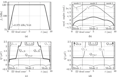
A nominal switching frequency of fs,nom = 120 kHz is selected to accommodate a compact converter design without causing excessive switching frequency related losses. Moreover, thermal limitations apply at high switching frequencies, resulting in an increased total converter volume. The frequency of 120 kHz is chosen to stay well below these thermal limits. Furthermore, it has been been shown in [25] that at both ends of the 10 ms half mains period, where the DAB input voltagevdc,1is low (see Figure2), it is beneficial to linearly reducefs. In these regions, ZVS is hard to achieve without making commutation inductances L1 and L2very small, which would result in unacceptably high circulating currents and thus a low conversion efficiency. This has led to the following predefined switching frequency pattern (see also Figure6(a)of Section3.4):
fs(Hz) = (
120 000 ifvdc,1>150 V, 75 000+375·(vdc,1−30) ifvdc,1<150 V.
(12)
3.3.2. Transformer Turns RatioN
A good design rule is to determine the turns ratioN = n1/n2of the HF transformer such that (N Vdc,2,min)>(vdc,1,max+10 V)[25]. Given the in- and output voltage range of the DAB converter, whereVdc,2,min=370 V andvdc,1,max=vˆac=358 V, this results in:
N>
v
dc,1,max+10 Vdc,2,min
=0.9946
→ N=1. (13)
3.3.3. Main Energy Transfer InductanceL
The maximum achievable DAB input currenthidc,1,maxiis obtained atτ1=τ2=πandφ=π/2, mode 2, and is given byhidc,1,maxi=N Vdc,2/(8fsL)[25]. This maximum current needs to be higher than the peak value of the ac input current at maximum power, which equal to ˆiac(=
√
2Iac,nom = √
2·16≈23 A). Therefore, the maximum allowable inductance valueLmaxis determined by:
Lmax=
N Vdc,2,min 8 fshidc,1,maxi
= 1·370
8·120000·23 =16.7µH. (14)
A good design guideline is to choose the valueLin the rangeL ≈(0.75 . . . 0.85)·Lmax[25], leaving sufficient margin for control purposes. This yields the final design value ofL=13µH.
3.3.4. Commutation InductancesL1andL2
As mentioned in Section3.3.1, there is a strong correlation between the lower value of fs(i.e. at lowvdc,1) and the maximum allowed values of commutation inductancesL1andL2. Determination of these values requires some iteration. AssumingL1=L2, the highest value forL1andL2that leads to full-operating-range ZVS, i.e. regarding the switching frequency pattern given by (12), has been found to beL1=L2=62.1µH, which is also the final design value.
3.4. Simulation Results
0 5 10 0
1 2
1.5 2.5
0.5
−0.5
(c)
0 5 10
0 1 2
1.5 2.5
0.5
−0.5
(d)
Figure 6. Resulting value trajectories of several quantities calculated for a half cycle of the nominal ac input voltage (Vac =230 Vrms, 50 Hz) at the nominal ac input current ofIac = 16 Arms(positive
power flow) and the nominal dc output voltage ofVdc,2=400 V.
Figure6(a). The modulation parametersx ={φ,τ1,τ2}that result from the simulation are shown in Figure6(b), expectedly comprising only switching modes 1 and 2. From Figures6(c)and6(d)it can be seen that the available commutation chargesQα,A/BandQδ,A/Bat the two most critical switching instantsθi = {α,δ} are higher than or equal to the minimum required commutation charges for achieving ZVS, i.e. respectivelyQreq,p(primary-side active bridge) andQreq,s(secondary-side active bridge). The same goes for the available commutation charges at the non-critical switching instants θi={β,γ} which are not shown for brevity. This means that ZVS of all the semiconductor devices is guaranteed in all operating points of the simulation run.
4. Modeling and Optimization of the Main Functional Elements
Based on the ZVS modulation scheme, the switching frequency pattern fs(vdc,1), and circuit variables h = {L,L1,L2,N} derived in Section3, in this section the main functional elements of the 1-S DAB ac–dc converter are designed and optimized. Each sub-section is dedicated to the design of the individual elements, combining state-of-the art design methods/procedures, models for the component losses, and volume models with custom developed component-level optimization algorithms in order to obtain a high-efficiency and high-power-density converter design that is in compliance with the system requirements specified in Table1. This implies separation of the partial converter functions and omission of outer optimization loops, i.e. with regard to the circuit level variables and the switching frequency.
4.1. Semiconductors and Heat Sinks 4.1.1. Semiconductor Selection
• A highly non-linear, not too big, parasitic output capacitance Coss, enabling ZVS turn-off and turn-on. TheCosscharacteristic of the FCH76N60NF MOSFETs is shown in Figure5(a);
• A low drain to source on-resistanceRDS(on)and a low junction to case thermal resistanceRth,J−C, being beneficial regarding the DAB’s conduction losses;
• A low total gate charge Qg, leading to reduced turn-on and turn-off times, improved ZVS behavior (fast turn-off) [30], and reduced gate drive losses;
• An integrated fast body diode with low reverse recovery charge Qrr and low reverse recovery timetrr, ensuring that all the energy will timely leave the transistor after a ZVS commutation. Of main importance for the four LF-switched MOSFETs of the SR are the characteristics that enable a reduction of the SR’s conduction losses, being a low on-resistanceRDS(on)and low junction to case
thermal resistanceRth,J−C. The switching-performance related characteristics are of less importance since the SR’s MOSFETs only change state two times per mains period. The STY112N65M5 (ST Microelectronics) MDmeshTM V power MOSFETs are chosen. TableA.1of Appendix A.1lists the most relevant device parameters of both the FCH76N60NF and the STY112N65M5 MOSFETs.
4.1.2. Loss Models
Since the modulation scheme derived in Section3.2results in full-operating-range ZVS of the DAB, switching losses can be neglected in the analysis [10,28]. Therefore, only conduction losses and the losses of the gate drive units are considered. For the SR also the gate drive losses can be neglected as the MOSFETs of the SR are low-frequency switched (100 Hz).
Conduction losses: The conduction losses of a MOSFET are proportional to the drain to source on-resistanceRDS(on)and to the squared RMS value of the conducted current4. Assuming a negligible junction temperature change within a full line cycleTL, the equivalent, line-cycle averaged conduction lossesPS,eq,cof a single MOSFET are determined by:
PS,eq,c=RDS(on)·IS,eq2 , (15) with: IS,eq= s
1 TL
Z TL
0 IS(t)dt. (16) IS is the local, switching-cycle averaged RMS value of the current conducted by the switch under consideration, and is used in (16) to calculate the equivalent, line-cycle averaged RMS valueIS,eq. In steady-state, each switch of the DAB conducts during half a switching cycleTs/2. As a result,IS,eqfor the switches of both active bridges are determined by:
ISS11-14,eq=
s 1 TL
Z TL
0 I√1(t)
2 dt, (17) ISS21-24,eq= s
1 TL
Z TL
0 I√2(t)
2 dt. (18)
I1andI2are the switching-cycle averaged RMS values of bridge currentsi1andi2. Each SR switch conducts during half a mains periodTL. Assuming that the HF components of the DAB input current idc,1are bypassed by HF filter capacitanceC1, for each SR switchIS,eqcan be approximated as:
ISSR1-4,eq≈
Iac √
2·PF. (19)
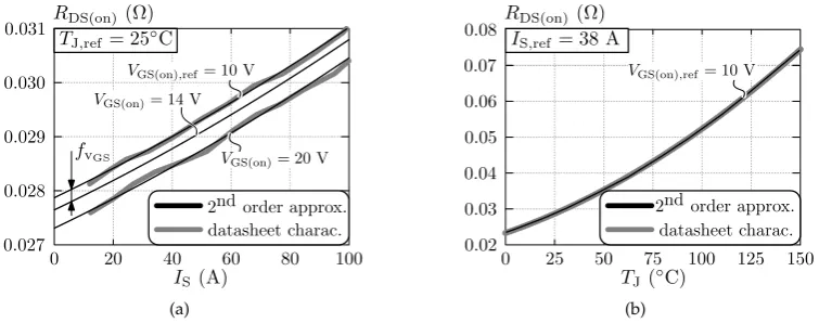
To calculate the resulting conduction losses using (15)-(19), the dependency of the MOSFET’s on-resistance on the junction temperatureTJand on the switch currentIShas to be modeled. Figure7 depicts these dependencies for the FCH76N60NF MOSFETs. The datasheet characteristics (gray lines) can be described by a 2ndorder approximation5(black lines) according to:
4 The conduction losses of the internal body diodes can be neglected as they only conduct current during a very small
interval of the switching periodTs.
(a) (b)
Figure 7. Dependency of the on-resistanceRDS(on)on (a) the switch currentISand (b) the junction
temperatureTJ, regarding the FAIRCHILD FCH76N60NF MOSFETs.
RDS(on)(TJ)|IS,ref,VGS(on),ref=a0+a1TJ,eq+a2T
2
J,eq, (20)
RDS(on)(IS)|TJ,ref,VGS(on),ref=b0+b1IS,eq+b2I
2
S,eq, (21)
where the equivalent, line-cycle averaged RMS valuesIS,eqfor the switches of active bridge 1, active bridge 2, and the SR are respectively given by (17), (18), and (19). TJ,eq is the equivalent, line-cycle averaged junction temperature of the switch under consideration:
TJ,eq = s
1 TL
Z TL
0 TJ
(t)dt, (22)
which is calculated using the thermal network model that will be presented in Section 4.1.3. The coefficients (a0,a1,a2andb0,b1,b2) required to evaluate (20) and (21) for both used MOSFET types are given in TableA.2of AppendixA.1whereTJ,ref,ID,ref, andVGS(on),ref are the datasheet reference values. By combining (20) and (21), a generalized equation can be found which expressesRDS(on)as
a function of the deviations∆TJ(= TJ,eq−TJ,ref) and∆IS(= IS,eq−IS,ref) of respectively the junction temperatureTJ,eqand the switch current IS,eqfrom the reference valuesTJ,refandIS,ref:
RDS(on)=hRDS(on)|TJ,ref,IS,ref,VGS(on),ref ·(1+α1∆TJ+α2∆T
2
J)·(1+β1∆IS+β2∆IS2) i
+fvGS. (23)
RDS(on) |TJ,ref,IS,ref,VGS(on),ref is the reference datasheet value as listed in Table A.1. The coefficients (α1, α2 and β1, β2) for both used MOSFETs are given in Table A.3. In (23) a displacement term fvGS, determined using linear interpolation (see Figure 7(a)), is introduced in order to take into
account the dependency of RDS(on) on the turn-on gate voltage VGS(on). For the FCH76N60NF
MOSFET, and regarding the applied turn-on gate voltage ofVGS(on) = 14 V, fvGS was found to be
fvGS = −2.247e
−4 Ω. For the STY112N65M5, f
vGS could not be calculated due to the absence of
information in the datasheet about the gate voltage dependency of RDS(on), and is assumed to be
zero. This leads to a negligible overestimation of the SR’s conduction losses.
Gate drive losses:Assuming an efficiency of 90% for the gate drive units (ηgd =0.9), the equivalent, line-cycle averaged gate drive lossesPS,eq,gare:
PSS11-24,eq,g=
1 ηgd
·Qg∆V 2 GS ∆VGS,ref
· 1 TL
TL
Z
0
(a) (b)
Figure 8.Heat sink - semiconductor assemblies for (a) the DAB and (b) the SR.
since the SR’s gate drive losses can be neglected. ∆VGSis the gate to source voltage swing which is 18 V (−4 . . .+14 V) for the custom designed gate drive circuits.Qgis the total (typical) gate charge, measured for the reference gate voltage swing∆VGS,refgiven in TableA.1of AppendixA.1.
4.1.3. Heat Sink Assembly and Thermal Network Model
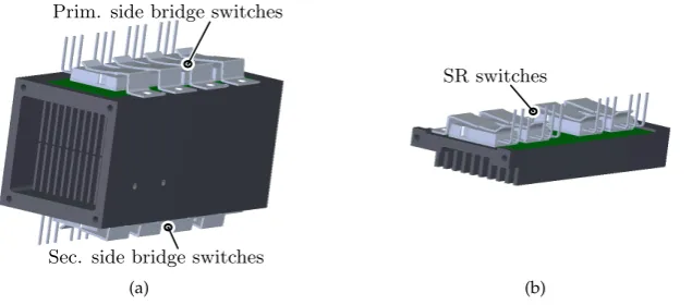
Autonomous air cooling by means of forced convection is one of the system requirements defined in Table1. Thereby the heat generated by the power devices is subtracted via a finned heat sink in combination with a fan. For the two active bridges of the DAB, a heat sink geometry with dual-sided base plate, as shown in Figure8(a), is considered. The four switches of the primary-side active bridge (active bridge 1; AB1) are mounted on the top-side base plate while the four switches of the secondary-side active bridge (active bridge 2; AB2) are mounted on the bottom-side base plate. The four switches of the SR are mounted on a heat sink geometry with single-sided base plate, as shown in Figure8(b). The resulting stationary heat transfer models are depicted in Figure9, where:
• Rth,J-C,Sxx are the junction to case thermal resistances of the switches;
• Rth,C-S,Sxx are the thermal resistances of the thermal pads (the Hi-Flow 300P thermal pads from
Bergquist are used for all switches).;
• Rth,S-Am,AB1andRth,S-Am,AB2(=Rth,S-Am,AB1) are the total thermal resistances between the surface of the heat sink (i.e. seen from one base plate) to the ambient, for the heat sink of the DAB;
• Rth,S-Am,SRis the total thermal resistance between the surface of the heat sink (i.e. the surface of the base plate) to the ambient, for the heat sink of the SR.
Rth,J-C,Sxxfor the used MOSFETs are given in TableA.1of AppendixA.1, whileRth,C-Sfor all switches
is defined by Rth,C-S = hpad/(λpadApad)where hpad is the thickness (hpad = 1.2e−4 m), λpad the thermal conductivity (λpad =1.6 W/mK), andApadthe cross section area of the thermal pads (Apad ≈ Apackage = 3.31e−4 m2 for the FCH76N60NF MOSFETs and Apad ≈ Apackage = 3.22e−4 m2 for the STY112N65M5 MOSFETs). Rth,S-Am,AB1 (= Rth,S-Am,AB2) and Rth,S-Am,SR are obtained from the heat sink optimizations performed in Section 4.1.4. Referring to Figure9, the equivalent junction temperatureTJ,eqof a switch can now be expressed as:
TJ,eq =TAm+PS,eq·(Rth,J-C+Rth,C-S+4·Rth,S-Am), (26) where, under the assumption that half the gate drive losses of a switch are internally dissipated in the switch while the other half is dissipated externally (i.e. in the gate drive units and gate resistors),
PS,eq=PS,eq,c+ PS,eq,g
2 . (27)
(a) (b)
Figure 9.Stationary heat transfer model of the heat sink assembly of (a) the DAB and (b) the SR.
semiconductor losses is available. Due to the interdependency of the quantities, a numerical solver is applied to solve:PS,eq= f(RDS(on), . . .),RDS(on)= f(TJ, . . .), andTJ= f(PS,eq, . . .).
4.1.4. Heat Sink Optimization
The surface-to-ambient thermal resistances Rth,S-Am,AB1 (= Rth,S-Am,AB2) and Rth,S-Am,SR of the forced-convection-cooled heat sinks are obtained from optimizations in which the heat sink geometries are determined in a way that, for a given fan and for given outer heat sink dimensions, these thermal resistances are minimized. This involves calculation of the thermal resistance for conductive heat transfer through the heat sink material, the thermal resistance for convective heat transfer, and the temperature increase of the air flowing through the heat sink channels. The applied optimization procedure and thermal models are described in detail in [31,32], and are summarized in the following, only considering stationary heat transfer. The involved variables6are given in Table2. For the heat sink geometry with dual-sided base plate shown in Figure8(a), the conductive and convective heat transfer are modeled according to Figure10. The thermal resistanceRth,S−Amfrom the base plate surface (index ‘S’) of this heat sink to the ambient (index ‘Am’), i.e. the air temperature at the heat sink inlet, is described by:
Rth,S-Am= 1
n (Rth,d+0.5(Rth,F/2+Rth,A/2)) +
0.5
ρAIRcp,AIR0.5 ˙VAF
, (28)
with:
Rth,d= d 1
n ABPλHS
, (29) Rth,F/2= 1 4c 1 2t LλHS
, (30) Rth,A/2= 1
h L12c. (31) For the heat sink geometry with single-sided base plate shown in Figure8(b), the conductive and convective heat transfer are modeled according to Figure11.Rth,S−Amis now described by:
Rth,S-Am= 1
n (Rth,d+0.5(Rth,F+Rth,A)) +
0.5 ρAIRcp,AIRV˙AF
, (32)
with:
Rth,d= d 1
n ABPλHS
, (33) Rth,F = 1 2c 1 2t LλHS
, (34) Rth,A= 1
h L c. (35)
6 Pr,ρ
AIR,νAIR, andλAIRare slightly temperature dependent. In order to simplify the analysis, the values at an average
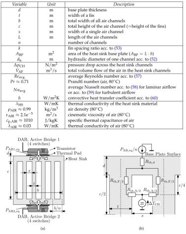
Table 2.Variables used for the calculation of the thermal resistance of a finned heat sink with fan, and for the calculation of the air flow rate in, and the pressure drop across the air channels of the heat sink.
Variable Unit Description
d m base plate thickness
t m width of a fin
b m total width of all air channels
c m total height of the air channel (=height of the fins) s m width of a single air channel
L m length of the air channels
n number of channels
k fin spacing ratio acc. to (53)
ABP m2 area of the heat sink base plate (ABP=L·b)
dh m hydraulic diameter of one channel acc. to (52)
∆pCH N/m2 pressure drop across the heat sink channels
˙
VAF m3/s total volume flow of the air in the heat sink channels
Reavg average Reynolds number acc. to (57)
Pr≈0.71 Prandtl number (air, 80◦C)
Nuavg average Nusselt number acc. to (58) for laminar airflow
or acc. to (59) for turbulent airflow
h W/m2K convective heat transfer coefficient acc. to (60)
λHS W/mK thermal conductivity of the heat sink material
ρAIR≈0.99 kg/m3 air density (80◦C)
νAIR≈2.1e−5 m2/s cinematic viscosity of air (80◦C)
cp,AIR≈1010 J/kgK specific thermal capacitance of air
λAIR≈0.03 W/mK thermal conductivity of air (80◦C)
(a) (b)
Figure 10. (a) Heat sink geometry with dual-sided base plate, considered to cool the switches of the DAB’s active bridges. (b) Thermal network describing stationary heat transfer between the surface of a base plate and the air in the heat sink channel (temperatureTCH).
The last term of the thermal resistance Rth,S−Am in both (28) and (32) considers the average temperature rise of the air from channel inlet to channel outlet. Calculation of the convective heat transfer coefficienth and the total volume flow ˙VAF of the air in the heat sink channels, which are both required for the calculation ofRth,S−Amin (28) and (32), goes as follows.
(a) (b)
Figure 11.(a) Heat sink geometry with single-sided base plate, considered to cool the switches of the SR. (b) Thermal network describing stationary heat transfer between the surface of the base plate and the air in the heat sink channel (temperatureTCH).
found as well. In case of laminar flow, with Re < 2300, eq. (58) is used to calculate the Nusselt number, which describes the convective heat transfer from the channel walls into the air. In case of turbulent flow, with Re > 2300, the Nusselt number is calculated with eq. (59). Using (60), the convective heat transfer coefficienthof the configuration is finally found.
By repeating the above procedure for different heat sink geometries, an optimal set of geometrical parameters (d,t,b,c,s,L, andn) can be found which leads to the lowest thermal resistance Rth,S-Am. This is done for both heat sinks, assuming predefined outer heat sink dimensions (i.e. variablesb,c,L, andd). As a result, the geometric parameters that are varied during the optimization are the number of channelsnand the fin spacing ratiok, which is equivalent to varying the channel widths; see eq. (53). The results are discussed below.
Heat sink of the DAB with dual-sided base plate, conform Figure10:The fan size defines the heat sink front geometry as only the fins that are facing the fan contribute to the convective heat transfer. After thorough iteration of the mechanical design of the final prototype converter, a 40x40 mm fan turned out to be most feasible, leading to the selection of the SanAce40GA7(see Figure12). Consequently, a heat sink geometry with b = c = 40 mm is most appropriate in order to fully utilize the fan. The pressure-flow curve,∆pFAN( ˙VAF), of this fan is depicted in Figure12(b)(gray line) and can be described by a 5thorder approximation (black line in Figure12(b)):
∆pFAN(V˙AF) =(5.38·1013·V˙AF5 −2.115·1012·V˙AF4 +1.96·1010·V˙AF3 −6.315·107·V˙2
AF+2.828·104·V˙AF+185.7).
(36)
The lengthLof the heat sink channels must be large enough so that sufficient space is provided on the base plates to mount the switches. Assuming a minimum spacing of 5 mm between the packages of adjacent switches, a minimum spacing of 10 mm between the base plate borders and a package, and a package width of approximately 16 mm for the TO-247 package, the minimum base plate length becomesLmin =3·5 mm+2·10 mm+4·16 mm= 99 mm. Preferably the maximum base plate length should not be much higher than Lmin, assuring homogeneous heat distribution across the base plate. The final base plate length isL=99.8 mm. The base plate thicknessdshould be
7 The SanAce40GA fan (type 9GA0412P7G001, see Figure12(a)) has been selected due to its high static pressure, high air
(a) (b)
Figure 12.(a) Picture of the selected fan: SanAce40GA, type 9GA0412P7G001, 40x40x15 mm, 12 V. (b) Datasheet pressure-flow curve (gray line) and 5thorder approximation (black line).
large enough to homogeneously spread the heat and small enough to limit the thermal resistance of the heat sink. The valued=6 mm is selected as a good trade-off between these two considerations.
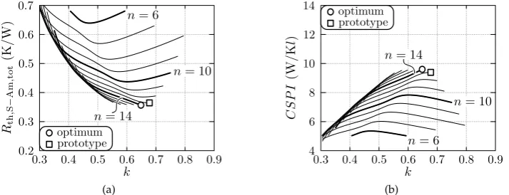
Figure 13 shows the results of the optimization, applying the assumed outer heat sink dimensions, i.e. the above discussed variablesb,c,L, andd, and assuming a minimum achievable fin thickness and channel width of 1 mm, which are enabled by using high-end milling machines. Furthermore, aluminium is considered for the heat sink material, defining the thermal conductivity valueλHS =210 W/mK. Figure13(a)depicts the relation betweenRth,S-Am,tot(=0.5·Rth,S-Am)8and the two geometric parametersnandkthat are independently varied. The performance indices and parameter values for the resulting (optimal) heat sink design are given in the top inset of TableA.4of AppendixA.1. There,VHSis the boxed volume of the heat sink, excluding the fan and an additional airflow inlet between the fan and the heat sink. VCS is the volume of the cooling system, including the heat sink, the fan, and an additional airflow inlet between the fan and the heat sink. CSPIis the cooling system performance index [31–33], which is an objective measure that allows to compare different cooling system designs with regard to power density. For the cooling system of the DAB, with dual-sided base plate,CSPIis defined as [32]:
CSPI= 1
Rth,S-Am,tot·VCS
= 1
0.5·Rth,S-Am·VCS. (37)
If a heat sink design shows aCSPIthat is two times higher than theCSPIof another one, the cooling volumeVCS can be made two times smaller for the same thermal resistance. Knowing that typical commercially available heat sink - fan combinations have aCSPIof around 5, the extensive heat sink optimization, achievingCSPI ≈ 9, is justified. The (boxed) volumeVCS,tot, which besides the heat sink, the fan, and the airflow inlet also includes the semiconductor switching devices, is also listed in TableA.4. The bottom inset of TableA.4shows the performance indices and design parameters of the heat sink used in the final (prototype) converter, and considered for further calculations. It in fact is a near-optimal design, which is due to the fact that the minimum achievable fin thickness and channel width were restricted due to limitations of the in-house manufacturing machines/tools.
Heat sink of the SR with single-sided base plate, conform Figure11: For the heat sink of the SR, once more the 40x40 mm SanAce40GA fan (see Figure12) is selected. As the SR requires less cooling effort than the DAB, the heat sink’s front geometry values are reduced fromb = c = 40 mm (most appropriate in order to fully utilize the fan) tob=36 mm andc=10 mm. This allows to use part of
8 The multiplication ofR
th,S-Amwith a factor ‘0.5’ is required sinceRth,S-Amis experienced from just one base plate of the
(a) (b)
Figure 13. Optimization result for the heat sink of the DAB (geometry with dual-sided base plate, cf. Figure10), assuming a minimum achievable fin thickness and channel width of 1 mm. (a) Total surface-to-ambient thermal resistanceRth,S-Am,tot(=0.5·Rth,S-Am) as function ofnandk, which are
independently varied. (b) Cooling system performance indexCSPIas function ofnandk.
the fan’s airflow to cool other electronic components. The reduced airflow in the heat sink channels due to the area reduction of the heat sink’s front geometry is taken into account by multiplying ˙VAF with the heat-sink-front-area to fan-area ratio (b·c)/(40·40). Furthermore, a slightly increased channel length of L = 104 mm is used and a base plate thickness ofd = 5 mm is applied. Once more, a minimum achievable fin thickness and channel width of 1 mm are assumed.
The performance indices and parameter values for the resulting (optimal) heat sink design are given in the top inset of TableA.5of Appendix A.1. The bottom table inset shows the values for the heat sink design of the final (prototype) converter. For the reason mentioned above this is a near-optimal design and is considered for further calculations. Note that the part of the fan that does not faces fins is not included in the calculation ofVCS,tot, and that for the heat sink with single-sided base plateCSPIis defined as [32]:
CSPI= 1
Rth,S-Am·VCS
. (38)
4.2. Magnetic Elements of the DAB: Inductors and Transformer
As mentioned before, the DAB dc–dc converter consists of three discrete magnetic elements: the HF ac-link transformer, the external series inductorLext, and the primary-side commutation inductor L1. The secondary-side commutation inductanceL2is implemented by the magnetizing inductance of the transformer (L2=LM), avoiding increased volume and costs. Referring to the equivalent DAB model shown in Figure3, the main energy transfer inductanceLis calculated with eq. (4), whereLσ,1 andLσ,2are the primary- and secondary-side leakage inductances of the transformer. Consequently, to determine the inductance valueLext, the transformer needs to be designed first (i.e. Lσ,1and Lσ,2 result from the final transformer design). Remind that the values ofL,L1,L2, andN(= n1/n2)are derived in Section3.3and are given in the right inset of Figure1.
4.2.1. Design and Optimization Procedure
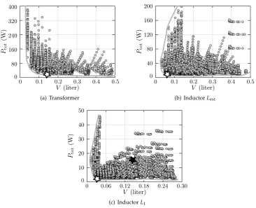
respect to the achievable power density [34,35]. All possible EELP and EILP core combinations from FERROXCUBE (ferrite core material: 3F3 and 3F4) and EPCOS (ferrite core material: N49, N87, N92, and N97) in the dimensions range from ELP32 up to ELP64 are considered. The number of stacked cores is limited by setting a maximum of 15 cm to the total core length. Litz wires are chosen to reduce eddy current losses in the windings [36–38], being particularly effective at high switching frequencies. Furthermore, four possible winding arrangements are investigated, including split, concentric, hexagonal and orthogonal type windings. Also the paralleling of several Litz bundles, as well as the interleaving (for the transformer) of the windings, is implemented in the algorithms.
All possible combinations of above mentioned design variables are top level iterated. For each iteration, in afirst stepthe reluctance model Rm of the considered magnetic element is calculated according to the methods proposed in [39], which inter alia provides a new analytical approach in order to determine the 3D air gap reluctance Rm,air. The inductance values, i.e. Lext, L1, and L2 (= LM), are controlled with the air gap length lg (constrained to 0 6 lg 6 lg,max = 1 mm), while guaranteeing that the peak flux density ˆBdoes not exceed a predefined maximum value ˆBmax. This introduces an upper and a lower limit to the possible number of turns. For the transformer, the minimum and maximum number of turns, i.e. n1,min respectively n1,max, for the primary-side winding are determined by:
n1,min =ciel
(V·s) p,max 2 ˆBmaxAc
, (39) n1,max=floor q
L0M(Rm,core+Rm,air)|lg=lg,max
, (40)
where(V·s)p,maxis the maximum primary-side referred Volt-seconds product,Acthe effective core cross section, Rm,core the core reluctance, Rm,air the air gap reluctance, and LM0 (= N2·LM) the primary-side referred magnetizing inductance. The number of turnsn1for the primary-side winding of the transformer then needs to be in the rangen1,min 6n 6n1,max. Evidently, the number of turns n2for the secondary-side winding is directly linked ton1via the transformer’s turns ratioN=n1/n2. For the inductors, the minimum and maximum number of turns, i.e.nind,minrespectivelynind,max, are determined by:
nind,min=ciel L
indiind,max ˆ
BmaxAc
, (41) nind,max=floor q
Lind(Rm,core+Rm,air)|lg=lg,max
, (42)
where iind,max is the peak inductor current and Lind (= Lext or L1) the inductance value of the considered inductor. The number of turns nind for the inductors then needs to be in the range nind,min 6 nind 6 nind,max. The upper boundary of the maximum allowed flux density ˆBmaxis set by the core material saturation flux densityBsatat a core temperature of 100◦C, applying a 30% safety margin. Subsequently, using an inner iteration loop, the number of turnsn1(transformer) is varied fromn1,minton1,maxwhile the number of turnsnind(inductors) is varied fromnind,mintonind,max.
In asecond step, a predefined objective function, which is determined by the sum of the core losses and the winding losses of the magnetic element at nominal operating conditions of the DAB, is minimized for each of above iterations. The applied loss models are summarized in Section4.2.2. The optimization algorithm used to minimize the cost function iterates the number of strands in the Litz bundles, as well as the diameter of the individual strands, in order to achieve a window filling that is optimal with regard to the winding losses. Thereby, constraint functions set restrictions on the positioning of the individual Litz bundles by bringing into relation the number of strands, the strand diameter, and wire positioning functions with the given core window area, taking into account creepage distances.
4.2.2. Loss Models
where∆Bis the peak-to-peak flux density. The Steinmetz parametersk,α, andβare extracted out of the core’s data sheets, providing information about the per-volume-unit core losses as a function of frequency f, peak flux density ˆB, and temperatureT. This enables extraction ofk,α, andβusing the empirical Steinmetz EquationPcore,V=k fαBˆβ, which is valid for sinusoidal excitation only.
Regardingwinding losses, the ohmic losses in the Litz wires (further referred to as Litz bundles) can be separated into skin effect losses PS from self-induced eddy currents inside the conductors, external proximity effect losses PP,efrom eddy currents due to the external magnetic field He that originates in the air gap fringing field and in the magnetic field from neighboring Litz bundles, and internal proximity effect lossesPP,ifrom eddy currents due to the internal magnetic fieldHi that is produced by the bundle itself. The per-unit-length (index ‘L’) skin-effect losses (including the dc losses) of a Litz bundle consisting ofnsstrands, are calculated with [38]:
PS,L=ns·Rdc,s,L·FR(f)· ˆ
I ns
2
, (45)
where ˆI are the Fourier amplitude coefficients of the total current in the Litz-wire bundle at the different harmonic frequencies f. Rdc,s,L is the per-unit-length dc resistance of a single strand: Rdc,s,L =4/(σπd2s), withdsthe diameter of the strand andσthe electric conductivity of the conductor material (σ=5.26·1071/Ωm for the considered Litz wires).FRis the skin-effect factor:
FR(f) = ξ
4√2·
ber0(ξ)bei1(ξ)−ber0(ξ)ber1(ξ) ber1(ξ)2+bei1(ξ)2
−bei0(ξ)ber1(ξ) +bei0(ξ)bei1(ξ) ber1(ξ)2+bei1(ξ)2
, (46)
withξ=ds/( √
2δ), whereδis the skin depth according toδ=1/pπ µ0σf.µ0is the permeability of the conductor material (µ0=4π10−7H/m for air and copper). The per-unit-length proximity losses in a Litz bundle are calculated as [38]:
PP,L=PP,e,L+PP,i,L=ns·Rdc,s,L·GR(f) Hˆe2+ ˆ I2 2π2d2b
!
. (47)
dbis the diameter of the Litz bundle whileGRis the proximity-effect factor:
GR(f) =− ξ π2d2s
2√2 ·
ber2(ξ)ber1(ξ) +ber2(ξ)bei1(ξ) ber0(ξ)2+bei0(ξ)2
+bei2(ξ)bei1(ξ)−bei2(ξ)ber1(ξ) ber0(ξ)2+bei0(ξ)2
. (48)
He is the external magnetic field that originates in the air gap fringing field and in neighboring Litz bundles, and is calculated using the 2D analytical approach proposed in [38]. This approach relies on an imaging and mirroring method in order to inter alia model the impact of a surrounding magnetic conducting material. Thereby the air gap fringing fields are modeled by means of fictitious conductors with eddy currents equal to the magneto-motive force across the air gap. Hi, with
ˆ H2
(a) Transformer (b) InductorLext
(c) InductorL1
Figure 14.Two-dimensional losses vs. volume performance spaces for (a) the HF ac-link transformer, (b) inductorLext, and (c) inductorL1, calculated for nominal DAB operating conditions.
4.2.3. Optimization Results
For each magnetic element of the DAB, the outcome of the optimization is a two-dimensional performance space, showing the losses at nominal operating conditions versus the (boxed) volume of the component. Figures14(a),14(b), and14(c)respectively depict the resulting performance spaces for the HF transformer and for inductorsLextand L1. The designs that are chosen for the hardware realization of the transformer and of inductorLextare marked withI. As these designs are located in the corner point of the so called ‘Pareto Front’, they are an optimal trade-off between efficiency and power density. It should be noted that the hardware realization ofL1, marked withH, is a duplicate of the HF transformer with one of the two windings removed and with the air gap length adapted according to the calculated inductance valueL1. The realization of L1 is thus non-optimal, and is referred to as the ‘prototype’ (prot.) design. A better solution would be to use the design marked with I, which is referred to as the ‘optimal’ (opt.) design. The detailed parameter values of the transformer and inductor designs are listed in TablesA.6-A.8of AppendixA.2, where TableA.8lists the values for both the ‘prot.’ and the ‘opt.’ design ofL1. The implication of using the improved design ‘opt.’ forL1on the converter performance is further discussed in Section5.
4.3. Output Filter Capacitors 4.3.1. LF Output Filter Capacitors
placed in parallel. This leads to a total LF output filter capacitance value ofC2,st = 1170 µF. For nominal conditions, i.e. Vac = 230 Vrms, Iac = 16 Arms, andVdc,2 = 400 V, this results in an very acceptable output voltage ripple amplitude of ˆ˜Vdc,2 ≈ 12 V. The worst case (i.e. atVac = Vac,max = 253 Vrms,Iac = Iac,nom = 16 Arms, andVdc,2= Vdc,2,min = 370 V) ripple amplitude is ˆ˜Vdc,2 ≈14.2 V, which is still less than 4% of the output voltage.
For the electrolytic LF output filter capacitors, with a diameter of 35 mm and a height of 40 mm (single capacitor), the total boxed volume is 0.147 liter. The part of the SR’s fan that does not faces heat sink fins is facing the LF filter capacitors, which are thereby cooled. Consequently, an additional volume of 0.024 liter is added to the LF capacitor’s volume for the system volume calculation in Section5. Remind that this part of the SR’s fan is not taken into account in the volume of the SR’s cooling system, see Section4.1.4.
4.3.2. HF Output Filter Capacitors
Besides the electrolytic LF capacitors, small HF filter capacitorsC2are placed at the output of the DAB in order to bypass the HF components of the DAB output currentidc,2. The HF filter capacitance value C2 is realized using seven 1.5µF, 630 V dc, metallized polypropylene MKP film capacitors, type B32674D6155, from EPCOS, which are placed in parallel. This leads to a total HF output filter capacitance value ofC2 = 10.5µF and a maximum HF output voltage ripple amplitude of less than 2 V. With a width of 31.5 mm, a depth of 12.5 mm, and a height of 19 mm (single capacitor), the total boxed volume is 0.052 liter.
4.3.3. Capacitor Losses
Losses in the LF filter capacitors are caused by their equivalent series resistance (ESR) and leakage current. The ESR value listed in the datasheet of the employed 390µF EETED2W391EA ELCOs from Panasonic is 0.34Ωat 120 Hz. According to the datasheet, the leakage currentIleakof a single capacitor is calculated asIleak =3·10−6·
√
C V(A), withCthe capacitance value inµF andV the capacitor voltage. Consequently, the total power lossPC2,stin the LF capacitors is calculated as:
PC2,st =3·(I
2
C2,st·ESR+Ileak·Vdc,2), (50)
whereIC2,st is the RMS value of the current in a single capacitor. The factor 3 is applied since three
capacitors are placed in parallel. Since the leakage current of polypropylene film capacitors is very low, the losses in the EPCOS HF capacitors are mainly caused by the ESR, producing a total loss of less than 0.5 W, which can be neglected.
4.4. EMC Input Filter
Figure 15.Schematic of the DM/CM EMC filters, connected to the synchronous rectifier of the ac–dc converter. Also shown are the line impedance stabilization network (LISN) and the EMC test receiver.
4.4.1. Differential Mode (DM) Filter Design
The DM EMC input filter is designed according to the procedure outlined in [42], and conform the guidelines given in [43] regarding filter damping, in order to comply with the CISPR 22 Class B standard [41] in the frequency range of 150 kHz – 30 MHz. The employed procedure includes the correct modeling of the line impedance stabilization network (LISN) and of the EMC test receiver (see Figure15), i.e. conform the CISPR 16 standard [44]. This enables a prediction of the measurement results and thus gives the basis for the calculation of the required attenuation and for the filter design. The video-filtered quasi-peak (QP) valuesVF(jω)at the output of the EMC test receiver need to be lower than the CISPR 22 Class B limit LimB(jω). For the case where no DM filter is present the most critical QP value is found9to beV
F,fcrit =170.4 dB·µV at a corresponding frequency
10 of f crit= 236.3 kHz, at which the Class B limit value is equal toLimB,fcrit =62.22 dB·µV. Therefore, the required
attenuationAttreq,fcrit of the DM filter, including a margin of 6 dB, is equal to:
Attreq,fcrit =VF,fcrit−LimB,fcrit+6 dB=170.4−62.22+6=114.18 dB. (51)
The DM filter needs to provide the required attenuationAttreq,fcritso that, in combination with an
appropriate CM filter, the converter complies with the standards. Thereby, control-oriented aspects have to be considered as well, ensuring a satisfactory operation of the converter. Using the recursive design procedure outlined in [42], the two-stage DM filter structure11 shown in Figure 15 turns out to be most appropriate for achieving these goals. In order to provide sufficient damping of the filter resonances without decreasing the attenuation in the frequency range that is relevant for compliance with the CISPR standard, for each filter stage an (optimized) passive damping network is employed. Thereby, a series inductor damping network with coupled inductors is selected for the
9 The simulations are performed under nominal operating conditions, i.e. at the nominal ac input voltage ofV
ac=230 Vrms,
the nominal ac input current ofIac=16 Arms, and an output voltage ofVdc,2=400 V. 10 Note that towards the dc side of the DAB’s input bridge, the bridge currenti
1is rectified intoidc,1, doubling the frequency.
Therefore, and due to operation with variable switching frequency, the value of 236.3 kHz forfcritcan be explained. 11 The components of the DM filter in Figure15are indexed ‘DM’ (i.e. ‘DM1’ for the first filter stage and ‘DM2’ for the second
Figure 16. Simulation of the QP measurement after insertion of the designed DM input filter and under the assumption of zero mains impedance. Also shown is the absolute lower boundary Minres(jω)for the measurement result and the CE limits according to CISPR 22 Classes A and B.
Figure 17.Simulated low-frequency harmonics of the mains currentiacand the IEC61000-3-2 limits.
first filter stage while a parallel capacitor damping network is used for the second filter stage. The resulting values and specifications of the employed DM filter components are listed in TableA.9of AppendixA.3. Note that the second filter stage is formed by capacitanceCDM2in combination with the LISN (RLISN = 50Ω,CLISN = 250 nF,LLISN = 50µH, see Figure15) and the mains inductance Lmains, i.e. no discrete inductorLDM2is present.
Figure16shows the simulated (nominal operating conditions) video-filtered quasi-peak (QP) values VF(jω) (indicated by a ‘I’), along with the CISPR 22 Classes A and B limits and the lower boundary value12 Minres(jω) after insertion of the designed DM input filter and under the assumption of zero mains impedance. It can be seen that the critical output valueVF,fcrit(indicated by
a ‘H’) is 6.67 dB lower than the Class B limit LimB,fcrit, meaning that compliance with the CISPR 22
Class B standard is achieved. Furthermore, the simulated low-frequency harmonics of the mains currentiac, which in the case at hand need to be below the limits defined in the IEC 61000-3-2 standard [45] for Class A equipment, are depicted in Figure17and are well below the limits.
4.4.2. Common Mode (CM) Filter Design
In order to successfully design a common mode (CM) filter that suppresses the CM noise on the earth wire, an equivalent CM noise-source model is required [46]. Thereby, detailed knowledge of the relevant parasitic impedances, through which the CM currents circulate, is essential. As a result, the design of the CM EMC filter is mostly performed after the realization of a first converter prototype
12 The curveMin
res(jω)is obtained as the square root of the sum of the squares of the RMS values of all harmonic components
system. The parasitic impedances can then be identified through impedance measurements and a CM noise propagation model can be derived. Consequently, several design iterations of the prototype system and/or the CM filter might be required until compliance with CISPR 22 Class B standard for conducted emission (CE) is obtained. Therefore, and as it is the DM filter and not the CM filter which mainly defines the EMC filter volume, the low-load power factor, and the dynamics of the system, here the detailed modeling of the CM filter is omitted. Nevertheless, a CM filter has been included in the converter hardware but, however, the selection of the filter architecture and the determination of the CM component values are based on intuition rather than on modeling and optimization. As can be seen from Figure15, in which the components of the CM filter are indexed ‘CM’ (i.e. ‘CM1’ for the first, ‘CM2’ for the second, and ‘CM3’ for the third filter stage), a three-stage CM EMC filter structure is employed. The final values and specifications of the CM filter components used in the converter prototype system are listed in TableA.10of AppendixA.3.
4.4.3. EMC Filter Losses and Volume
The hardware realization of the CM and DM EMC input filter can be seen in Figure18(b)of the next section. With a width of 132 mm, a height of 72 mm, and a depth of 25 mm, the total boxed volume of the filter board is 0.238 liter. This volume includes the converter’s ac connection terminals and an ac fuse, the converter’s dc connection terminals and a dc fuse, a 2-electrode surge arrestor (type EC600-X, EPCOS), and several metal oxide varistors. An additional volume of 0.042 liter is occupied by six CM filter capacitors that are placed on another PCB, yielding a total EMC filter volume of 0.279 liter. Since the leakage current of polypropylene film capacitors is very low, the losses in the EPCOS HF EMC filter capacitors are mainly caused by the ESR, producing a total loss of less than 0.4 W. Consequently, the losses in the EMC filter capacitors can be neglected. The same goes for the losses (less than 0.1 W) in damping resistorsRDM1,d andRDM2,d, and for the core losses of the DM inductors. Therefore, the main contributors to the overall losses of the EMC input filter are the losses due to dc resistance of the CM and DM inductor windings.
5. Hardware Demonstrator and Calculated Performance
Based on the loss and volume models, and on the results of the component optimizations presented in Section4, in this section the performance of the 1-S DAB ac–dc converter is calculated in terms of losses (& efficiency) and volume (& power density). The results are obtained under the assumption of TAm = 22◦C ambient temperature since this has also been the test condition (see Section6). The 3.7 kW hardware demonstrator, being realized in accordance with the design and optimization results of Section4, is shown in Figure18. It should be mentioned that the primary-side commutation inductanceL1was originally not included in the hardware design. During testing L1 was connected to the converter with the screws that are located on the top power PCB. Nevertheless, the volume of this inductor is included in the results for the system’s volume and power density. Below, the calculated performance is presented for two converter designs which only differ from each other by the implementation of the primary-side commutation inductorL1:
• Converter design A; prototype converter; uses the design ‘prot.’ (prototype) for L1. This is how the hardware demonstrator is implemented;
• Converter design B; further optimized; uses the improved design ‘opt.’ (optimal) for L1 (see Section4.2.3). This design yields higher conversion efficiencies and power density compared to converter design A.
(a)
(b)
Figure 18.3.7 kW, 1-S, single-phase, bidirectional, and isolated DAB ac–dc hardware demonstrator.
‘prot.’ (prototype converter), implying that a substantial performance enhancement of the hardware demonstrator would be possible by replacingL1.
By summation of the losses of the individual components, the overall converter losses are calculated which are shown in Figure19for both converters designs A (prototype; see Figure19(a)) and B (further optimized; see Figure 19(b)). As expected, the latter design yields a substantial overall loss reduction. Note that the calculated overall converter losses include the auxiliary power losses, which comprise the power consumption of the fans and of the control board. These losses are estimated to be approximately 7 W. Figure20shows the resulting overall conversion efficiency, which for design A (prototype; see Figure20(a)) is above 95% for input powers higher than 20% of the nominal input power, with a very flat efficiency curve and thus a high partial-load efficiency. The peak efficiency is around 96.1% and the efficiency at nominal input power approximately 95.6%. From Figure20(b)it is clear that, at all power levels, an important efficiency enhancement is feasible (up to around 0.8%) when considering converter design B with optimized inductorL1.
Table 3.Converter power density values (at 3.7 kW, nominal input power).
Design A (Prot.) Design B (Opt.) V(liter) ρ(kW/liter) V(liter) ρ(kW/liter)
Incl. ‘other + dead space’ 1.87 2 1.76 2.1
Excl. ‘other + dead space’ 1.47 2.5 1.36 2.7
(a) (b)
Figure 19. Calculated total losses of the 1-S DAB ac–dc converter implemented according to (a) converter design A (prototype converter) and (b) converter design B (further optimized).
(a) (b)
Figure 20. Calculated efficiency of the 1-S DAB ac–dc converter implemented according to (a) converter design A (prototype converter) and (b) converter design B (further optimized).
Figure21shows the loss contribution of the different converter components for both converter designs A (prototype; dark gray bars) and B (further optimized; light gray bars). Figure 21(a) corresponds with the nominal ac input voltage ofVac = 230 Vrms, the nominal ac input current of Iac=16 Arms, and the nominal dc output voltage ofVdc,2=400 V. Figure21(b)corresponds with the same voltage conditions but reduced ac input current ofIac=0.2·Iac,nom=3.2 Arms.
Figure 22 shows the volume contribution of the different converter components for both converter designs A (prototype; dark gray bars) and B (further optimized; light gray bars), calculated using the boxed component volumes derived in Section4. The bars ‘total, excl. other’ represent the summation of the component volumes while the bars ‘total, incl. other’ represent the total boxed volume of the complete converter system, including the ‘dead space’ and the volume of the remaining electronic components such as the measurement circuits, the PCBs, and the gate drive units. The volume reduction of 0.107 liter achieved for converter design B results from the smaller size of the optimized primary-side commutation inductorL1.
(a)
(b)
Figure 21. Loss contribution of the different converter components for both converter designs A (prototype; dark gray bars) and B (optimized; light gray bars) atVac = 230 Vrms, Vdc,2 = 400 V
for (a)Iac=Iac,nom=16 Arms(100% power) and (b)Iac=0.2·Iac,nom=3.2 Arms(20% power).
Figure 22. Volume contribution of the different converter components for both converter designs A (prototype; dark gray bars) and B (optimized; light gray bars).
6. Measurements
The 3.7 kW hardware demonstrator shown in Figure 18is successfully tested within the full power range (up until an output power of 3.7 kW), showing ac waveforms with little distortion, and which are in very good agreement with the waveforms obtained from simulations. For illustration, Figure23depicts the measured waveforms at the ac and dc side of the converter at nominal ac input voltage ofVac=230 Vrms, nominal ac input current ofIac=16 Armsand 450 V dc output voltage. The conversion efficiency and the converter’s ac input power quality are evaluated using the Yokogawa WT3000 precision power analyzer, having a power accuracy reading of±0.02 %.
Figure24shows the measured performance of the converter with regard to the reached efficiency and with regard to the quality of the ac input power. The measured efficiency (Figure24(a); solid lines) corresponds well with the efficiency calculated in Section5(see dashed lines). Although the trends match very well, a slight discrepancy (mostly less than 0.4%) can be noticed between the calculated and the measured efficiencies. This might require further refinement of the loss models developed in Section 4, especially regarding possible non-zero ZVS losses of the MOSFETs. The measured efficiencies are higher than 95% within the major part of the output power range, with a very flat efficiency curve and thus a high partial-load efficiency. The peak efficiency is around 96.1% and the efficiency at nominal output power approximately 95.6% (see curve for the nominal output voltage ofVdc,2 = 400 V). As predicted by the calculations, only a minor difference (around 0.25-0.3% at maximum) can be noticed between the efficiency curves at different output voltages, i.e. the efficiency is highest for the lowest output voltage and lowest for the highest output voltage. Furthermore, as can be seen in Figure24(b)a (true) power factor (PF) close to unity, and a low total harmonic distortion (THD) of the ac input current of around 4%, are obtained within the major part
Figure 23.Measured waveforms at the ac and dc side of the converter at nominal ac input voltage of Vac=230 Vrms, nominal ac input current ofIac=16 Armsand 450 V dc output voltage. Voltage and
current scale:vac: 100 V/div.,iac: 12.5 A/div.,Vdc,2: 150 V/div.,hidc,2i: 7.5 A/div.
(a) (b)
Figure 24. Measurement of (a) the efficiency and (b) the total harmonic distortion THD and (true) power factor PF. The measurements are taken at the nominal ac input voltage ofVac =230 Vrms, in
Figure 25. Comparison of the efficiency of the presented 1-S DAB ac–dc converter (black line; converter A) and the efficiency of two state-of-the-art dual-stage converter systems reported in literature: converter B presented in [47] and converter C presented in [48].
of the output power range and within the whole output voltage range. This makes that, regarding conversions efficiency, system power density, PF, and THD, the converter requirements specified in Table1of the introduction are achieved, confirming the competitiveness of the investigated 1-S DAB ac-dc converter.
For completeness, Figure25compares the efficiency of the presented 1-S DAB ac–dc converter (black line; converter A) with the efficiency of two state-of-the-art dual-stage converter systems reported in literature. The efficiency obtained is substantially higher than that of the converter presented in [47] (converter B; Si MOSFETs & SiC diodes), while the converter presented in [48] (converter C) has the highest efficiency but, however, is not bidirectional. The power density reached with converter A (2 kW/liter, this work) is substantially higher than the 0.66 kW/liter power density of converter B while converter C has the highest power density of 2.5 kW/liter.
7. Conclusion
In this paper a single-stage (1-S) converter approach is analyzed to realize a single-phase, bidirectional, isolated ac–dc converter, combining all functionalities into one conversion stage and thus enabling a cost-effective efficiency and power density increase compared to traditional dual-stage (2-S) ac–dc converters. The converter topology consists of a quasi-lossless synchronous rectifier followed by an isolated DAB dc–dc converter, putting a small filter capacitor in between.
In a first step, the operating principle/conditions of the 1-S ac–dc converter are presented, the available modulation parameters and relevant switching modes of the DAB are detailed, and the method used for calculating an efficient full-operating-range ZVS modulation scheme is summarized. The selection of the high-level circuit variables such as the switching frequency, the inductance values, and the transformer’s turns ratio is outlined as well.
whole output voltage range. This makes that, regarding conversions efficiency, system power density, PF, and THD, the predefined (automotive) converter requirements are met.
Lastly, the performance of the presented 1-S DAB ac–dc converter is compared with the performance of two state-of-the-art dual-stage converter systems reported in literature. Therefrom, it can be concluded that the achieved efficiency and power density are very close to the absolute state-of-the-art, confirming the competitiveness of the investigated 1-S converter architecture, especially since it is shown that a further efficiency increase of up around 0.8 % and a further power density increase of 0.1 kW/liter is feasible by a simple improvement of one of the inductor designs (i.e. commutation inductorL1). Evidently, an even higher efficiency and/or power density is enabled by use of gallium nitride (GaN) or silicon carbide (SiC) semiconductor devices.
Acknowledgments:Costs to publish this paper in open access are covered by the Electromechanics and Power Electronics (EPE) group of the Eindhoven University of Technology (TU/e).
The author wants to acknowledge the division of Electrical Energy and Computer Architectures (ELECTA) of the University of Leuven (KU Leuven; Leuven, Belgium), and in particular Prof. dr. ir. Johan Driesen for the support provided. The author also wants to acknowledge Tiphase N.V. (Leuven, Belgium), and in particular dr. Jeroen Van den Keybus for the support provided.
Conflicts of Interest:The author declares no conflict of interest.
Abbreviations
The following abbreviations are used in this manuscript:
1-S: Single-Stage 2-S: Dual-Stage
BEV: Battery Electric Vehicle CE: Conducted Emission CM: Common Mode
CSPI: Cooling System Performance Index DAB: Dual Active Bridge
DM: Differential Mode ELCO: Electrolytic Capacitor EMC: Electromagnetic Compatibility ESR: Equivalent Series Resistance HF: High-Frequency
iGSE: improved Generalized Steinmetz Equation LF: Low-Frequency
LISN: Line Impedance Stabilization Network
MOSFET: Metal Oxide Semiconductor Field-Effect Transistor PF: Power Factor
PFC : Power Factor Correction PHEV: Plug-in Hybrid Electric Vehicle QP: Quasi-Peak
RBW: Resolution Bandwidth SR: Synchronous Rectifier TCM: Triangular Current Mode THD: Total Harmonic Distortion V2G: Vehicle-to-Grid