Article
1
Optimization of Line-Tunneling Type L-Shaped
2
Tunnel Field-Effect-Transistor for Steep
3
Subthreshold Slope
4
Faraz Najam 1 and Yun Seop Yu 1,*
5
1 Department of Electrical, Electronic and Control Engineering and IITC, Hankyong National University
6
* Correspondence: [email protected]; Tel.: +81-31-670-5293
7
8
Abstract: Recently L-shaped tunneling field-effect-transistor (LTFET) has been introduced to
9
overcome the thermal subthreshold limit of conventional metal-oxide-semiconductor
10
field-effect-transistors (MOSFET). In this work, shortcoming of LTFET was investigated. It was
11
found that corner effect present in LTFET effectively degrades its subthreshold slope. To get rid of
12
corner effect a new type of device with dual material gates is presented. The new device termed as
13
DG-LTFET gets rid of the corner effect and results in a significantly improved subthreshold slope
14
of less than 10 mV/dec, and an improved ON/OFF current ratio over LTFET. In this work
15
DG-LTFET was evaluated for different device parameters, and bench-marked against LTFET. This
16
work presents an optimum configuration of DG-LTFET in terms of device dimensions and doping
17
levels, to get the best subthreshold, ON current and ambipolar performance from the DG-LTFET.
18
Keywords: Band-to-band tunneling, L-shaped tunnel field-effect-transistor, double-gate tunnel
19
field-effect-transistor, corner-effect.
20
21
1. Introduction
22
Tunnel field-effect-transistors (TFET) are being actively pursued as a potential replacement to
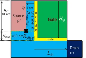
23
conventional complementary metal-oxide-semiconductor (CMOS) technology [1]. TFETs offer
24
sub-thermal subthreshold slope (SS) but suffer from limited ON current ION performance [2]. To
25
overcome the limit, recently different types of line tunneling type TFETs have been introduced
26
including L-shaped TFET [3] (LTFET), U-shaped [4] (UTFET), and Z-shaped [5] TFET (ZTFET).
27
Among them, only LTFET has been experimentally demonstrated [3].
28
It was found using device simulations that 2-dimenasional (2D) corner effect [6] present in
29
LTFET degrades its subthreshold performance. In order to remove SS degradation due to the kink
30
effect induced by the source corner, the fully depleted rounded corner with gradual doping profile
31
was used [6]. LTFET still achieves sub-thermal SS but as shown in this work there is room for
32
significant improvement in the subthreshold performance of LTFET. To achieve this improvement, a
33
new device based on the original LTFET is introduced in this work. The new device uses a dual-gate
34
(DG) structure, and is termed as DG-LTFET. The two gates (gate1 and gate2) have different
35
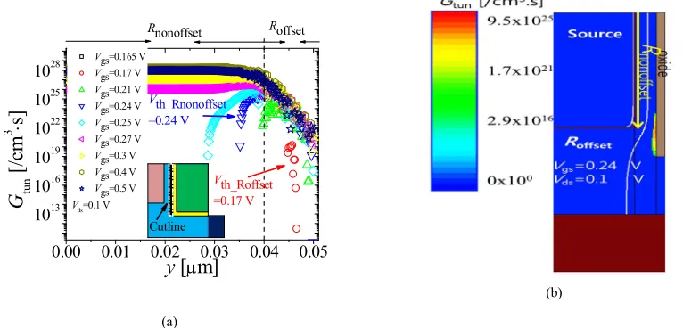
workfunctions and different heights. DG-LTFET was thoroughly evaluated for different device
36
parameters including the source region height, gate1 and gate2 heights, gate1 and gate2
37
workfunctions, channel thickness, and drain doping levels. Optimum dimensions and drain doping
38
level were determined for the DG-LTFET. Section 2 briefly discusses the corner-effect problem of
39
LTFET. Section 3 introduces DG-LTFET, and compares its results with LTFET. Section 4 presents
40
conclusion.
41
42
2. LTFET: Corner Effect
43
Fig. 1 shows a schematic for LTFET. The p+ (1020 cm-3) doped source region overlaps the gate
44
with the n- (1012 cm-3) channel sandwiched in between them. This sandwiched channel region is
45
termed as Rnonoffset. Also, there is a part of the channel termed as Roffset in which there is an offset
46
present between the source and the gate as indicted in Fig. 1. The following parameters were used
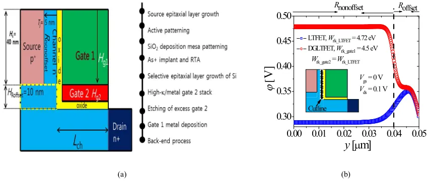
47
for all devices considered in this work unless otherwise specified. Source height (Hs) = 40 nm, oxide
48
thickness (tox) = 2 nm, length of Rnonoffset (Tj) = 5 nm, channel length (Lch) = 50 nm, height of Roffset (Hoffset)
49
= 10 nm, height of Rnonoffset (Hnonoffset) = Hs, gate height (Hg1) = Hs + (Hoffset - tox) = 48 nm, dielectric
50
permittivity ox = 25, metal gate workfunction Wrk_LTFET = 4.72 eV, and drain doping (Nd) = 1020 cm-3.
51
52
Sentaurus technology-computer-aided-design tool (TCAD) was used as the simulator [7]. The
53
following models were used in the simulation: dynamic nonlocal band-to-band-tunneling (BTBT)
54
model, fermi statistics, and constant mobility model. Dynamic nonlocal BTBT model calculates
55
BTBT in both lateral and 1-dimensional (1D) directions. Crystal orientation is assumed to be <100>
56
in all devices. A constant electron effective tunneling mass of 0.19 mo was used in all simulations [8].
57
All simulation were done at drain source bias Vds = 0.1 V unless otherwise specified.
58
59
For analysis to follow, drain-source current (Ids) versus gate-source bias (Vgs) characteristics of
60
the LTFET are shown in Fig. 2(a). There is a direct overlap between gate and source in Rnonoffset, and
61
the electric field in Rnonoffset is in 1D direction. However, in Roffset, electric field from the gate
62
converges around the sharp source corner marked by an X in Fig. 1. This increases the potential in
63
Roffset as compared to Rnonoffset for any given bias (until potential saturates due to electron inversion).
64
Fig. 2(b) shows the surface potential at Vgs = 0 V. It can be seen that because the electric field
65
Figure 1. Schematic of LTFET.
0.0 0.1 0.2 0.3 0.4 0.5 0.6 10-17
10-14 10-11 10-8 10-5
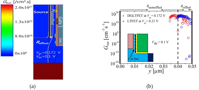
0.00 0.04 0.08 0.12 0.16 0.20
Vth_Roffset=0.17 V Vth_Rnonoffset
=0.24 V
Rnonoffset
+
RoffsetI ds
[
A
]
I ds
[
A
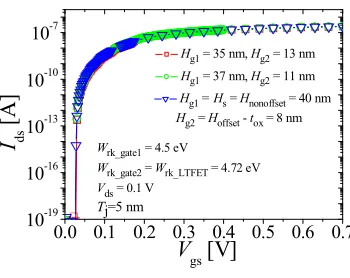
]
Vgs [V]
Vds=0.10 V
Only Rnonoffset
(a)
0.00 0.01 0.02 0.03 0.04 0.05 0.28
0.32 0.36
Roffset
[V]
y [m] Rnonoffset
Vgs=0 V
Vds=0.1 V
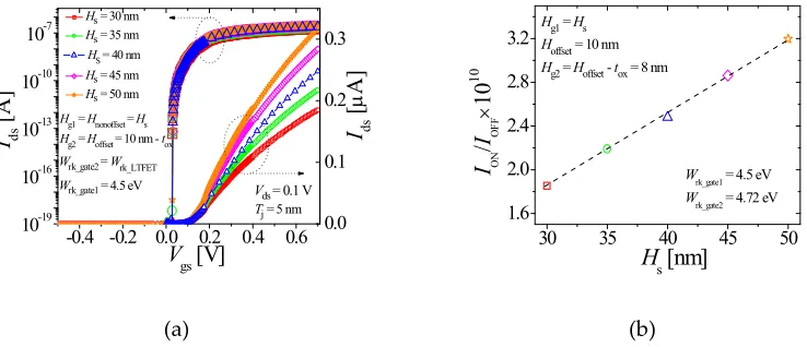
Cutline
(b)
Figure 2. (a). Ids-Vgs transfer characteristics of LTFET. Indicated are Vth_Rnonoffset = 0.24 V, and Vth_Roffset
converges around the sharp source corner [6], the potential in Roffset has increased. Since the
66
potential is higher in Roffset as compared to Rnonoffset, the threshold voltage for BTBT in Roffset (Vth_Roffset)
67
is lower than the threshold voltage for BTBT in Rnonoffset (Vth_Rnonoffset).
68
Figs. 3(a) and (b) show the tunneling rate (Gtun) contour plot and Gtun, respectively at Vgs = 0.21
69
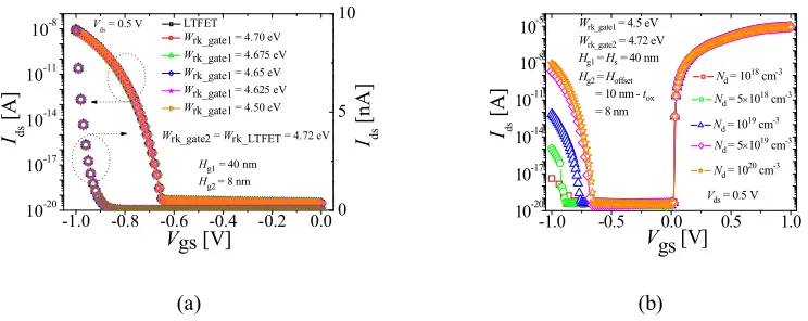
V which is the bias needed to generate Ids = 10-13 A (from Fig. 2(a)). It is obvious from Fig. 3 that the
70
BTBT only takes place in Roffset whereas Rnonoffset is completely switched off. Fig. 4(a) shows Gtun at
71
several Vgs values. From Fig. 4(a) Vth_Roffset and Vth_Rnonoffset can be found to be around Vgs = 0.17 and
72
0.24 V, respectively. Fig. 4(b) shows Gtun contour plot at Vgs = Vth_Rnonoffset = 0.24 V. It can be noticed
73
from Fig. 4(a) that Gtun in Rnonoffset just after it turns on, is always higher and has much larger BTBT
74
area (in y direction) as compared to Roffset. Thus whenever Rnonoffset turns on, it dominates over Roffset.
75
The reason why Gtun is higher in Rnonoffset is simply because the BTBT paths in Roffset are laterally
76
oriented or 2D from source to the surface in Roffset, whereas the BTBT paths in Rnonoffset are 1D. The
77
2D BTBT paths being naturally longer than the 1D paths result in lower Gtun in Roffset.
78
79
80
From Fig. 4(a), it can be observed that for a large part of the subthreshold region (Vgs < 0.24 V)
81
only Roffset with the longer 2D BTBT paths and lower Gtun is contributing to the BTBT current and the
82
more efficient Rnonoffset makes no contribution to the current. In other words, LTFET underperforms
83
in the subthreshold region. If Rnonoffset could be forced to turn on at a lower bias than Roffset that is the
84
0.00 0.01 0.02 0.03 0.04 0.05 101
106 1011 1016 1021
Roffset
Gtu
n
[
/c
m
3.s
]
y [m]
Vgs=0.21 V
Vds=0.10 V
Cut line
Rnonoffset
(a) (b)
Figure 3. (a) Gtun contour plot at Vgs = 0.21 V, which is the bias needed to generate Ids = 10-13 A and (b)
Gtun extracted from Fig. 3(a).
0.00 0.01 0.02 0.03 0.04 0.05 1013
1016 1019 1022 1025 1028
Vgs=0.165 V Vgs=0.17 V Vgs=0.21 V Vgs=0.24 V Vgs=0.25 V Vgs=0.27 V Vgs=0.3 V Vgs=0.4 V
Vgs=0.5 V Vds=0.1 V
Vth_Rnonoffset
=0.24 V
Roffset
G
tun
[
/c
m
3
s]
y
[
m]
Rnonoffset
Vth_Roffset
=0.17 V
Cutline
(a)
(b)
Figure 4. (a) Gtun at different Vgs. Indicated in Fig. 4(a) are Vth_Rnonoffset = 0.24 V, and Vth_Roffset = 0.17 V
and (b) Gtun contour plot at Vgs = Vth_Rnonoverlap = 0.24 V. In Fig. 4(b), yellow arrow indicates the height
condition Vth_Rnonoffset < Vth_Roffset, Rnonoffset will turn on in the subthreshold region, and with the
85
condition, Gtun in Rnonoffset > Gtun in Roffset, demonstrated in Fig. 4(a), a significant improvement in SS
86
could be expected.
87
3. DG-LTFET
88
3.1. DG-LTFET: Basic Device Physics
89
In order to achieve the condition Vth_Rnonoffset < Vth_Roffset, DG-LTFET is presented in Fig. 5(a).
90
DG-LTFET uses dual material gates denoted by gate1 and gate2, each with a different workfunction
91
(Wrk_gate1/2) and height (Hg1/2). Hg1 = Hnonoffset = Hs = 40 nm, Hoffset = 10 nm, Hg2 = Hnonoffset - Hg1 + (Hoffset -
92
tox) = 8 nm, and Tj = 5 nm. Wrk_gate1 is always lower than Wrk_gate2. Wrk_gate2 is fixed at Wrk_LTFET = 4.72 eV
93
for all DG-LTFET considered in this work. DGLTFET process-flow is indicated in Fig. 5(a). The
94
process-flow is based on LTFET process-flow [3]. DGLTFET process-flow follows LTFET
95
process-flow until the metal-organic chemical vapor deposition of gate 2 (similar to gate deposition
96
in LTFET). After this two additional steps are required. The device is masked to protect the gate
97
oxide and channel areas, and gate 2 is selectively etched according to desired height. Metal of Gate
98
1 is then deposited in the recess created by gate 2-etching. Similar dual-material gate structures
99
have been extensively reported in the literature including [9-11].
100
Lower Wrk_gate1 results in an increased flatband voltage (Vfb) [12] in Rnonoffset as compared to Roffset.
101
Fig. 5(b) shows Vfb of DG-LTFET (red symbols) with Wrk_gate1 = 4.5 eV and Wrk_gate2 = Wrk_LTFET. Also Vfb
102
of LTFET (blue symbols) is shown for reference. Expectedly DG-LTFET potential increases in
103
Rnonoffset. The potential does not change abruptly from gate1 to gate2 because of the presence of 2D
104
effects around the source corner. Electric field from bottom of gate2 converges around the source
105
corner. Around the middle of Roffset, equilibrium is established between the two gates and
106
DG-LTFET potential overlaps LTFET potential since Wrk_gate2 = Wrk_LTFET. With Wrk_gate1 < Wrk_gate2, the
107
increased potential in Rnonoffset reduces Vth_Rnonoffset. If Wrk_gate1/2 are appropriately tuned with Wrk_gate1 <
108
Wrk_gate2, the condition Vth_Rnonoffset < Vth_Roffset = 0.17 V could be achieved. Because Wrk_gate2 = Wrk_LTFET =
109
4.72 eV, Vth_Roffset (in DG-LTFET) is equal to Vth_Roffset (in LTFET).
110
111
(a)
0.00 0.01 0.02 0.03 0.04 0.05 0.30
0.35 0.40 0.45 0.50
LTFET, Wrk_LTFET = 4.72 eV
DGLTFET, Wrk_gate1 = 4.5 eV
Wrk_gate2 = Wrk_LTFET
Roffset
V
]
y
[
m]
RnonoffsetVgs = 0 V
Vds = 0.1 V
Cutline
(b)
Figure 5. (a) Schematic of DG-LTFET with process-flow indicated alongside and (b) Vfb of
DG-LTFET (red symbols) compared with that of LTFET (blue symbols). In DG-LTFET, Wrk_gate1 = 4.5
Figs. 6(a), (b), and (c) show Ids-Vgs characteristics at different Wrk_gate1, SS, and ION/IOFF of
112
DG-LTFET with constant Wrk_gate2 = Wrk_LTFET = 4.72 eV for all DG-LTFET, respectively. Also the Ids-Vgs
113
characteristics of LTFET (black squares) are shown for reference. ION is extracted at Vgs = 0.7 V, and
114
IOFF is defined as Ids = 10-17 A. With Wrk_gate1 = 4.675 eV (red circles), the Vth_Rnonoffset is reduced to 0.189
115
V. Compared with LTFET, Rnonoffset now turns on earlier in the subthreshold region, along with Roffset.
116
Since BTBT is more efficient in Rnonoffset (Fig. 4(a)) as compared to Roffset, Ids increases more rapidly
117
within the subthreshold region. Hence, just at the transition point, where Rnonoffset turns on (Vgs ~
118
0.189) a kink appears in the Ids-Vgs curve. With Wrk_gate1 = 4.65 eV (green triangles), Vth_Rnonoffset is
119
reduced to Vgs = 0.167 V and the condition Vth_Rnonoffset < Vth_Roffset is achieved and DG-LTFET exhibits a
120
remarkable SS with values less than 10 mV/dec as seen in Fig. 6(b). With Wrk_gate1 = 4.625 eV (blue
121
stars), Vth_Rnonoffset reduces further to 0.1448 V which is < Vth_Roffset. If Vth_Rnonoffset < Vth_Roffset is established
122
than any increase in Vth_Roffset – Vth_Rnonoffset simply shifts the Ids-Vgs to the left without any change in SS
123
as shown by the blue stars (Wrk_gate1 = 4.625 eV) and orange diamonds (Wrk_gate1 = 4.5 eV) in Figs. 6(a)
124
and (b), respectively. An improvement of ~16 % is observed in ION/IOFF of DG-LTFET (with Wrk_gate1 =
125
4.625 eV) over LTFET.
126
127
0.0 0.2 0.4 0.60.0 0.1 0.2 0.3
Vgs [V]
LTFET
Wrk_gate2 = 4.72 eV
Kink
10-19 10-15 10-11 10-7 10-3
Ids
[
A
]
Wrk_gate1 = 4.65 eV
Ids
[
A
]
Wrk_gate1 = 4.675 eV
IOFF =10 -17
A
Vds=0.1 V Tj=5nm
Wrk_gate1 = 4.625 eV
Wrk_gate1 = 4.5 eV
(a)
100-15 10-14 10-13 10-12 10-11 10
20 30 40 50
Ids [A] LTFET Wrk_gate1 = 4.675 eV
Wrk_gate1 = 4.65 eV
Wrk_gate1 = 4.625 eV
Wrk_gate1 = 4.6 eV
SS [mV
/dec]
(b)
4.50 4.55 4.60 4.65 4.70 1.8
2.0 2.2 2.4 2.6
4.50 4.55 4.60 4.65 4.70
ION
/
IOF
F
1
0
1
0
Wrk_gate1 [eV] ION@Vgs=0.7 V IOFF=10-17 A
Wrk_gate2=Wrk_LTFET
Hg1=Hs=40 nm
Hg2=8 nm
Hoffset=10 nm
(c)
Figure 6. (a). Ids-Vgs characteristics of DG-LTFET with different Wrk_gate1s and fixed Wrk_gate2 = Wrk_LTFET.
Also shown is Ids-Vgs characteristics of LTFET (black squares). (b) SS extracted from Ids-Vgs
characteristics in Fig. 6(a). (c) ION/IOFF ratio extracted from Ids-Vgs characteristics in Fig. 8(a). Red
circles: Wrk_gate1 = 4.675 eV, Green triangles: Wrk_gate1 = 4.65 eV, Blue stars: Wrk_gate1 = 4.625 eV, Orange
128
Fig. 7(a) shows Gtun contour plot of DG-LTFET at a Vgs (= 0.172 V) bias needed to achieve an
129
equivalent Ids of 10-13 A in DG-LTFET with Wrk_gate1 = 4.65 eV. Fig. 7(b) shows contour plot extracted
130
from Fig. 7(a). For reference Fig. 7(b) also shows Gtun needed to generate an equivalent amount of Ids
131
in LTFET (at a Vgs bias of 0.21 V, Fig. 3(b)). As can be seen in Fig. 7(b), LTFET needs contribution
132
only from Roffset, but to generate the same amount of Ids, DG-LTFET depends heavily on Rnonoffset with
133
some contribution from Roffset. Because Gtun in Rnonoffset is more efficient (Fig. 4(a)), as the Vgs bias
134
increases, Gtun increases exponentially in a much larger area in Rnonoffset which results in the
135
DG-LTFET exhibiting a much steeper subthreshold swing, while the LTFET continues to depend
136
only on the inefficient BTBT in Roffset until around Vth_Rnonoffset = 0.24 V.
137
3.2. Device Optimization
138
To optimize device performance, impact of variations in key parameters including Hg1/2, Hs/Tj,
139
and Nd was investigated. To investigate the impact of Hg1/2 values, Ids-Vgs characteristics for
140
DG-LTFET at different Hg1 and Hg2 = Hnonoffset - Hg1 + (Hoffset - tox) with fixed Wrk_gate1 = 4.5 eV and
141
Wrk_gate2 = Wrk_LTFET, Hs = Hnonoffset = 40 nm, Hoffset = 10 nm, and Tj = 5 nm is presented in Fig. 8. It can be
142
seen that Ids is independent of Hg1/2.
143
(a)
0.00 0.01 0.02 0.03 0.04 0.05 10-24
10-14 10-4 106 1016
1026 DGLTFET at V
gs= 0.172 V LTFET at V
gs= 0.21 V
Roffset
Gtun
[cm
-3 s -1 ]
y [m]
Vds = 0.1 V
Cut line
Rnonoffset
(b)
Figure 7. (a) Gtun contour plot of DG-LTFET with Wrk_gate1 = 4.65 eV at Vgs = 0.172 V, which is
needed to generate Ids = 10-13 A and (b) Gtun extracted from Fig. 7(a) (red symbols). Also Gtun (blue
symbols) of LTFET at a Vgs bias needed to generate Ids = 10-13 A are shown for reference. In Fig. 7(a),
144
Next, to investigate the effect of Tj on device performance, Ids-Vgs characteristics, SS, and ION/IOFF
145
of DG-LTFET are presented for different Tj with fixed Wrk_gate1 = 4.5 eV and Wrk_gate2 = Wrk_LTFET, Hg1 =
146
Hnonoffset = 40 nm, Hoffset = 10 nm. and Hg2 = Hnonoffset - Hg1 + (Hoffset - tox) = 8 nm in Fig. 9(a), (b) and (c),
147
respectively. It was found that the increasing Tj results in a degradation of ION/IOFF ratio. It is simply
148
because of the increase in BTBT path length with the increase in Tj. Tj of 5 nm was found to be
149
optimum in this work as any further reduction will bring significant quantum confinement effect
150
into play which is well known to degrade device performance [4-5], [13-15].
151
Next, the impact of varying Hs is investigated. Ids-Vgs characteristics of DG-LTFET for several Hs
152
with fixed Wrk_gate1 = 4.5 eV and Wrk_gate2 = Wrk_LTFET, Hg1 = Hs = Hnonoffset, Hg2 = Hnonoffset - Hg1 + (Hoffset - tox)
153
= 8 nm, and Tj = 5 nm is presented in Fig. 10. By maintaining Hg1 = Hs, Hoffset =10 nm, and Hg2 = 8 nm,
154
the electric field vector distribution within DG-LTFET remains the same as Hs is varied, and BTBT
155
area simply scales with Hs. An increase (decrease) in BTBT area with Hs simply results in an
156
increased (decreased) ION/IOFF ratio as shown in Fig. 10(b) with no change in SS as evident from Fig.
157
10(a).
158
159
160
0.0 0.1 0.2 0.3 0.4 0.5 0.6 0.7 10-19
10-16 10-13 10-10 10-7
I ds
[
A]
V
gs [V]
Hg1 = 35 nm, Hg2 = 13 nm
Hg1 = 37 nm, Hg2 = 11 nm
Hg1 = Hs = Hnonoffset = 40 nm
Hg2 = Hoffset - tox = 8 nm
Wrk_gate1 = 4.5 eV
Wrk_gate2 = Wrk_LTFET = 4.72 eV Vds = 0.1 V
Tj=5 nm
Figure 8. Ids-Vgs characteristics for several Hg1/2s with Wrk_gate1/2 = 4.5 eV and Wrk_gate2 = Wrk_LTFET. Red
161
162
Finally, ambipolar current of DG-LTFET is discussed. Ambipolar Ids of TFET depends on
163
drain-channel junction. In DG-LTFET, drain-channel junction is controlled by gate2 with Wrk_gate2 =
164
Wrk_LTFET. With the same workfunction, the electrostatics of drain-channel junction in DG-LTFET is
165
exactly the same as that in LTFET. Fig. 11(a) shows ambipolar Ids of DG-LTFET compared with
166
LTFET. Any change in Wrk_gate1 in DG-LTFET does not affect the drain-channel junction. Same
167
argument applies for any other design parameter variation in DG-LTFET including Hs, Hg1/2, Tj, that
168
is, as long as electrostatics of drain-channel junction remains unaffected, DG-LTFET will exhibit
169
equivalent ambipolar Ids as LTFET. Further, impact of Nd on ambipolar Ids was considered. Different
170
Nd values were considered for a DG-LTFET with Wrk_gate1 = 4.5 eV and Wrk_gate2 = Wrk_LTFET, Hg1 =
171
Hnonoffset = 40 nm, Hg2 = Hoffset ̶ tox = 8 nm, and Tj = 5 nm and the results are shown in Fig. 11(b).
172
Drain doping level of 1018 cm-3 was found to suppress ambipolar Ids appreciably without affecting
173
the ION.
174
175
0.0 0.2 0.4 0.6 10-17
10-14 10-11 10-8 10-5
Hoffset=10 nm
Ids
[
A
]
Ids
[
A
]
V gs [V]
Tj = 5 nm
Hg1 = Hs = 40 nm Hg2 = 8 nm
Tj = 6 nm Wrk_gate2 = Wrk_LTFET
Tj = 7nm
Wrk_gate1 = 4.5 eV
Vds= 0.1 V
0.0 0.1 0.2 0.3
(a)
100-17 10-16 10-15 10-14 10-13 10 S S [ m V /d ec ]
Ids [A]
Tj = 5 nm Tj = 6 nm
Wrk_gate2 = Wrk_LTFET = 4.72 eV
Wrk_gate1= 4.5 eV
Tj = 7 nm
(b) 0.5 1.0 1.5 2.0 2.5 IO N / IO FF x 1 0 1 0
Wrk_gate_1=4.5 eV Wrk_gate_2=Wrk_LTFET ION@Vgs=0.7 V IOFF=10-17 A
5.0 5.5 6.0 6.5 7.0 T
j [nm]
(c)
Figure 9. Ids-Vgs characteristics of DG-LTFET with different Tj and fixed Wrk_gate1 = 4.5 eV, Wrk_gate2 =
Wrk_LTFET and Hg1 = Hs = Hnonoffset = 40 nm, Hg2 = Hoffset (10 nm) - tox = 8 nm. (b) SS of Ids-Vgs shown in Fig.
8(a). (c) ION/IOFF ratio of Ids-Vgs characteristics shown in Fig. 8(a). Red squares, green circles, and blue
triangles: Tj = 5, 6 and 7 nm, respectively.
-0.4 -0.2 0.0 0.2 0.4 0.6 10-19
10-16 10-13 10-10 10-7
Wrk_gate1 = 4.5 eV
Wrk_gate2 = Wrk_LTFET
I ds
[
A]
Ids
[
A]
Vgs [V]
Hs = 30 nm
Hs = 35 nm
Hs = 45 nm
Hs = 50 nm
Vds = 0.1 V
Hg1 = Hnonoffset = Hs
Hg2 = Hoffset = 10 nm - tox
0.0 0.1 0.2 0.3
HS = 40 nm
Tj = 5 nm
(a)
30 35 40 45 50
1.6 2.0 2.4 2.8 3.2
I ON
/
I OF
F 1 0 1 0
Hs [nm]
Hg1 = Hs Hoffset = 10 nm
Hg2 = Hoffset - tox = 8 nm
Wrk_gate1 = 4.5 eV
W
rk_gate2 = 4.72 eV
(b)
Figure 10. Ids-Vgs characteristics of DG-LTFET with different Hs, fixed Wrk_gate1 = 4.5 eV, Wrk_gate2 =
Wrk_LTFET, and Hg1 = Hs = Hnonoffset, Hg2 = Hoffset (= 10 nm) - tox = 8 nm. (b) ION/IOFF ratio of Ids-Vgs
characteristics shown in Fig. 10(a). Red squares, green circles, blue triangles, magenta diamonds,
176
5. Conclusions
177
Device physics of LTFET were investigated. It was found that a large part of subthreshold
178
region is dominated by the parasitic, lateral, and 2D BTBT from source to Roffset with lower Gtun. The
179
more efficient 1D BTBT from source to Rnonoffset, which has higher Gtun, takes place at a higher bias in
180
the subthreshold region because of Vth_Rnonoffset > Vth_Roffset. The device does not utilize its channel fully
181
during the subthreshold region due to Vth_Rnonoffset > Vth_Roffset. A new type of device based on LTFET
182
was introduced in this work. The device uses a dual gate-stacked structure which workfunction of
183
upper gate Wrk_gate1 is below that of lower gateWrk_gate2. This makes the potential in Rnonoffset increase
184
and thus Vth_Rnonoffset reduce. DG-LTFET reverses the threshold condition of LTFET, which it lowers
185
Vth_Rnonoffset (< Vth_Roffset). Rnonoffset with higher Gtun turns on earlier than Roffset in the subthreshold region
186
of DG-LTFET and the device exhibits SS of less than 10 mV/dec. It was found that Wrk_gate1 in
187
DG-LTFET needs to be sufficiently less than Wrk_gate2 to achieve the sub 10 mv/dec SS. It was found
188
that Ids and SS are independent of Hg1/2. DG-LTFET was further evaluated for different device
189
dimensions including Tj and Hs, while maintaining the electric field vector distribution equivalent.
190
Ids decreases with an increase in Tj and scales with Hs. Nd value of 1018 cm-3 was found to appreciably
191
reduce ambipolar Ids. With the results presented in this work DG-LTFET could be considered as a
192
viable potential replacement to conventional MOSFET.
193
Author Contributions: Conceptualization, N.F., and Y.S.Y.; methodology, N.F, and Y.S.Y.; investigation, N.F.,
194
and Y.S.Y; data curation, N.F.; writing—original draft preparation, N.F.; writing—review and editing, N.F., and
195
Y.S.Y.; supervision, Y.S.Y.; project administration, Y.S. Y.; funding acquisition, Y.S.Y.
196
Funding: This research was funded by Ministry of Trade, Industry & Energy (MOTIE), project number
197
10054888 and Korea Semiconductor Research Consortium (KSRC) support program for the development of
198
future semiconductor devices.
199
Acknowledgments: This work was supported by IDEC (EDA tool).
200
Conflicts of Interest: The authors declare no conflict of interest. The funders had no role in the design of the
201
study; in the collection, analyses, or interpretation of data; in the writing of the manuscript, or in the decision to
202
publish the results.
203
204
-1.0 -0.8 -0.6 -0.4 -0.2 0.0
10-20 10-17 10-14 10-11 10-8
I ds
[
n
A
]
I ds
[
A
]
Vgs [V] LTFET
Wrk_gate1 = 4.70 eV Wrk_gate1 = 4.675 eV Wrk_gate1 = 4.65 eV Wrk_gate1 = 4.625 eV Wrk_gate1 = 4.50 eV
Wrk_gate2 = Wrk_LTFET = 4.72 eV V
ds = 0.5 V
Hg1 = 40 nm
H
g2 = 8 nm
0 5 10
(a)
-1.0 -0.5 0.0 0.5 1.0
10-20 10-17 10-14 10-11 10-8
10-5 Wrk_gate1 = 4.5 eV
Wrk_gate2 = 4.72 eV
Hg1 = Hs = 40 nm
Hg2 = Hoffset
= 10 nm - tox
= 8 nm
I ds
[
A
]
Vgs [V]
Nd = 1018 cm-3
Vds = 0.5 V
Nd = 51018 cm-3
Nd = 1019 cm-3
Nd = 51019 cm-3
Nd = 1020 cm-3
(b)
Figure 11. (a) Ids-Vgs characteristics of DG-LTFET at Vds = 0.5 V with different Wrk_gate1 and Wrk_gate2 =
Wrk_LTFET, Hg1 = Hoffset = 10 nm, Hg2 = 8 nm, Tj = 5 nm and Nd = 1020 cm-3. Red circles, green triangles,
blue diamonds, magenta stars, and orange right triangles: Wrk_gate1 = 4.7, 4.675, 4.65, 4.625, and 4.5
eV. (b) DG-LTFET Ids with different Nd. Nd = 1018 cm-3 demonstrates almost negligible ambipolar Ids.
Red squares, green circles, blue triangles, magenta diamonds, and orange stars: Nd = 1018, 51018,
References
205
1. Avci, U. E.; Morris, D. H. Tunnel field-effect transistors. IEEE J. Electron Devices Soc. 2015, 3, 88-95, doi:
206
10.1109/JEDS.2015.2390591.
207
2. Ionescu, A.M.; Riel, H. Tunnel field-effect transistors as energy efficient electronic switches. Nature 2011,
208
479, 329-337, doi: 10.1038/nature10679.
209
3. Kim, S. W.; Kim, J. H.; Liu, T. K.; Choi, W. Y.; Park, B. Demonstration of L-shaped tunnel field-effect
210
transistors. IEEE Trans. Electron Devices 2016, 63, 1774-1778, doi: 10.1109/TED.2015.2472496.
211
4. Yang, Z. Tunnel field-effect transistor with an L-shaped gate. IEEE Electron Device Lett.2016, 4, 839-842,
212
doi: 10.1109/LED.2016.2574821.
213
5. Imenabadi, R. M.; Saremi, M.; Vandenberghe, W. G. A novel PNPN-like Z-shaped tunnel field-effect
214
transistor with improved ambipolar behavior and RF performance. IEEE. Trans. Electron Devices 2017, 64,
215
4752-4758, doi: 10.1109/TED.2017.2755507.
216
6. Kim, S. W.; Choi, W. Y.; Sun, M. C.; Park, B. G. Investigation on the corner effect of L-shaped tunneling
217
field-effect transistors and their fabrication method. J. Nanosci. Nanotechnol. 2016, 9, 6376-6381, doi:
218
10.1166/jnn.2013.7609.
219
7. Sentaurus User Manual, version L-2016.03, Mar. 2016.
220
8. Kao, K. H.; Verhulst, A. S.; Vandenberghe, W. G.; Soree, B.; Groeseneken, G.; Meyer, K. D. Direct and
221
indirect band-to-band-tunneling in germanium-based TFETs. IEEE Trans. Electron Devices 2012, 59,
222
292-301, doi: 10.1109/TED.2011.2175228.
223
9. Saxena, R. S.; Kumar, M. J. Dual-material gate technique for enhanced transconductance and breakdown
224
voltage of trench power MOSFETs. IEEE. Trans. Electron Devices 2009, 56, 517-522, doi:
225
10.1109/TED.2008.2011723.
226
10. Long, W.; Ou, H.; Kuo, J-M.; Chin, K. K. Dual-material gate (DMG) Field Effect Transistor. IEEE. Trans.
227
Electron Devices 1999, 46, 865-870, doi: 10.1109/16.760391.
228
11. Polishchuk, I.; Ranade, P.; King, T-J.; Hu, C. Dual work function metal gate CMOS technology using
229
metal interdiffusion. . IEEE Electron Device Lett. 2001,9, 444-446, doi: 10.1109/55.944334.
230
12. Sze S.M.; Kwok, K. Ng. Physics of Semiconductor Devices, 3rd ed.; John Wiley & Sons: Hoboken, New Jersey,
231
USA, 2006; ISBN: 9780471143239.
232
13. Walke, A. M.; Verhulst, A. S.; Vandooren, A.; Verreck, D.; Simeon, E.; Rao. V. R.; Groeseneken, G.;
233
Collaert, N.; Thean, A. V. Y. Part I: Impact of field-induced quantum confinement on subthreshold swing
234
behavior of line TFETs. IEEE Trans. Electron Devices 2013, 60, 4057-4064, doi: 10.1109/TED.2013.2287259.
235
14. Padilla, J. L.; Gamiz, F.; Godoy, A. A simple approach to quantum confinement in tunneling field-effect
236
transistors. IEEE Electron Device Lett. 2012, 33, 1342-1344, doi: 10.1109/LED.2012.2207876.
237
15. Padilla, J. L.; Alper, C.; Gamiz, F.; Ionescu, A. M. Assessment of field-induced quantum confinement in
238
heterogate germanium electron-hole bilayer tunnel-field transistor. Applied Physics Letters 2014, 105,
239
082108-1 082108-4, doi.org/10.1063/1.4894088.
240