IJSRSET17361 | Received : 16 Oct 2017 | Accepted : 31 Oct 2017 | September-October-2017 [(3)6: 986-991]
© 2017 IJSRSET | Volume 3 | Issue 6 | Print ISSN: 2395-1990 | Online ISSN : 2394-4099 Themed Section: Engineering and Technology
986
Development of Front End Electronics for Nuclear
Spectrometer
Vaishnavi G1 , Dipak Kumar Panda2 ,Velraj G3
1,3Department of Physics, Anna University, Chennai, Tamilnadu, India 2Dipak panda Kumar, Physical Research Laboratory, Ahmedabad, Gujarat, India
ABSTRACT
Gamma Ray spectrometer is an instrument to be used for measurements of elemental abundance of elements like Si, Mg, Ca, Ti, Fe, Al, K, U, and Th etc. We have developed the front end electronics for this spectrometer. Various types of detector are used for the gamma ray spectrometer. In this paper we have discussed the development design and its simulation results. In the current design we have used an low cost, high bandwidth and high slew rate to minimize the noise.
Keywords:
Preamplifier, Multisim, Noise Measurement, PMT, Spectrometer.
I.
INTRODUCTION
Gamma Ray spectrometer (GRS) is a well establish technique used to find out the elemental abundance of element like Si, Mg, Ca, Ti, Fe, Al, K, U, and Th etc. For the laboratory measurement GRS is mainly used to measure the concentration of natural radioactive element like K, U and Th. While in Planetary Science, it is mainly used for remote sensing study. Using GRS, the concentration of elements like Si, Mg, Ca, Ti, H, Fe, Al, K, U, and Th etc. can be measured. Nuclear spectroscopy very useful field of Medical imaging and
Therapeutic, Astronomy, Geochemistry, Atomic
physics, HEAO (High energy Astronomy Observatory) investigation.
The solar system objects (Planets, satellite of planets or asteroids) having no atmosphere or very thin atmosphere like Mars can emit gamma ray from their surface which can be detected using gamma ray spectrometer. The gamma ray from the planetary bodies are produced either by interaction with galactic cosmic ray or by decay of radionuclide elements. When galactic cosmic ray interacts with the planetary bodies it produces secondary particle along with high energy neutron. These secondary neutrons again interact with the surface material and produce gamma ray either by inelastic scattering or neutron capture methods. Gamma ray also produced by the decay of natural radioactive
element like K, U and Th. Gamma rays produced via interactions with major rock-forming elements (e.g., iron, silicon, aluminum and magnesium,) provide essential information for geochemical studies.
For Planetary application generally a gamma ray
spectrometer with high gamma-ray detection
efficiencies, as well as good energy resolutions are preferred to detect and distinguish contributions from different elements. For development of Gamma ray spectrometer. Scintillation crystals and semiconductor detector are used. Semiconductor detectors are mostly used because of its ability to provide very good energy resolution, provided they are cooled to liquid nitrogen (-77 K). Whereas scintillation crystals are well popular detector used for the detection of gamma ray. Though scintillation detector provides very poor energy resolution but their main advantage is that they don‟t need any cooling mechanism. Some of the new developed scintillation crystal especially rare earth halide crystals like LaBr3: Ce, LaCl3: Ce and CeBr3 provide comparable better energy resolution than the other scintillation detector.
scintillation detector produces visible light and then the scintillation detector is coupled with a PMT (photomultiplier tube) which produces the charge. In solid-state detectors, the photon interactions are collected directly from charge production. The collected charge is converted to a voltage pulse by a preamplifier. The pre-amplifier output is amplified using linear amplifier for the pulse height analysis. The amplified output is then digitized and energy information of gamma event is read through multichannel analyze (MCA). The block schematic for gamma ray processing is shown in figure-1.
Fig. 1 Basic functional block of gamma ray spectroscopy.
In this front end electronics process is consist of amplification, shaping and ADC module. In this amplification process is convert week signal into strong signal which done by preamplifier and amplifier and noise filter. so here introduce high bandwidth and low noise op-amp design for amplification and shaping.
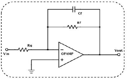
Fig. 2 Basic diagram of charge amplifier
Preamplifier can be classified into 3 types: charge sensitive, current sensitive and parasitic-capacitance. With semiconductor detector generally the Parasitic-capacitance preamplifiers are not used because the gain of this type of preamplifier is sensitive to small changes
in the parasitic capacitance. Current sensitive
preamplifier mostly used for timing application [2]. The charge sensitive preamplifier preferred for most energy spectroscopy application. The signals from the radiation
detector are generally represented as quantity of quantity of charge delivered as a current pulse durable from ns to µs depending on the type of detector used. For most of the application it is important to know the quantity of charge & the time of occurrence of an event. A standard diagram for charge sensitive preamplifier is shown in figure-2 provide both the information. As
shown in fig-1 it integrates the charge on the Cf
(feedback capacitor), as a results its gain is not sensitive to a change in detector capacitance (Cin). In ideal case,
the rise time of the output pulse is equal to the detector current pulse width.
The output voltage from the preamplifier can be written as
where QD is the charge released by the detector, Cf is the
feedback capacitor, and Rf is the feedback resistor.
Rf is a noise source in direct-coupled system, and
therefore a charge sensitive preamplifier is introduced. It gives high gain, integration linearity, low noise, temperature stability, high speed rise time, etc. In the current work we have designed the current system derived from simulation of charge sensitive preamplifier using Multisim software [1].
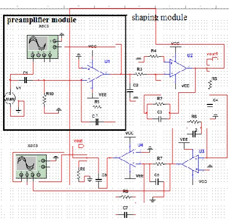
Design and Operation of Preamplifier Module
As earlier mentioned the gamma ray events are represented as charge pulse and which are then converted into voltage pulse by preamplifier. Output pulse from preamplifier proportional to the total integrated charge pulse.
The basic feedback pre-amplifier design is shown in figure-1. The Rf is generally kept high to reduce the
International Journal of Scientific Research in Science, Engineering and Technology (ijsrset.com)
Fig. 3 LT 1252 Pin connections
Fig 4. Design of preamp module with shaping module for gamma ray spectrometer.
We can improve the low noise by keeping high value of feedback resister and it plays main role in noise source
of DC system. By keeping input capacitor (Cin) is high,
feedback capacitor clipping problem will reduce. We have simulated the performance of pre-amplifier using Multisim. In the simulations we have taken the output at various stages. The pulse output of the from the detector and the preamplifier are measured across the detector capacitor C1(adjust in µF)and the feedback resistance
R1(which is in M) respectively. The pre-amplifier
output is amplified to a Gaussian shape using same LT
1252 op-amp with CR-RC2 combination. The output of
different stage of amplification are measured the output terminals of the corresponding amplifier. In the simulation we have used a Power supply in pulse voltage source [3].
TABLEI.
SPECIFICATION OF OP-AMP USED FOR WORK
S.No List of Property Op-AmpLT1252
1 Bandwidth 150MHz
2 Slew Rate 400 V/µS
3 Power Supply Range + 2.5 to + 15 V
4 Settling Time 90ns to 0.1%
5 Noise Distortion In
Current/Voltage
V- 7.5nV/√Hz
C- 1.5pA/√Hz
6 I/P Impedance 357 Ω
7 Gain 5 stable
8 Supply Current 7mA
II.
SHAPING MODULE
A Gaussian shaping amplifier module is used to read out the “tail pulse” signals such as from PMTs, charge sensitive preamplifiers and other similar detection system. In general, the Gaussian shaping amplifiers are known as „linear amplifiers‟, „spectroscopy amplifiers‟, „pulse amplifiers‟. The function of these amplifiers is not only to transform the shape of the event pulse from Gaussian function, but also to filter much of the noise from the signal of interest. By using a shaping amplifiers will reduce the fall time of the pulse signals, dropping the incidence of pulse „pile up‟, and improve the SNR of the detection system as shown in figure-5.
Fig. 5 Diagram of Shaping amplifier
In our simulation we have used the CR-RC2mode of
Fig. 6 Result of input and input capacitor
According to the input of voltage signal, capacitor which connected with detector provides the charging and discharging pulse. The output of voltage across the capacity C1 reaches to its maximum i.e. 2.4vwhen t is 5ms. Operating mode depends on charge collection time tc and the input time constant RC1. R1C1>> tc detector
capacitance discharges slowly. Vout can be calculate
from preamplifier as fallows
( ) (1)
Where = RfCf the time constant.
The simulation output of preamplifier has been shown in figure 7.
Fig. 7 Charge sensitive amplifier output at 1ststage.
Furthermore, shaping output is semi Gaussian shape with good peak time. The simulation out has been shown in figure-8.
Fig 8. shaping amplifier output
III.
IV ANALYSES
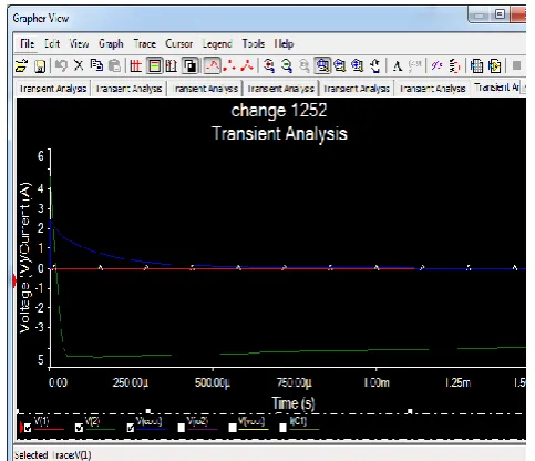
A. Transient Analysis
This process as a method of studying the nature of something or of determining its essential features and their relations in the design. Transient analyses can determine the charging and discharging process in time domain. Transient analysis is most useful for studying fault conditions in the circuit, like short circuits, overloads, etc. From this optimized design not have a short circuit, overload, having proper charging and discharging.
International Journal of Scientific Research in Science, Engineering and Technology (ijsrset.com)
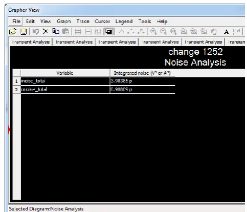
B. Noise Analyses
Multisim creates a noise model of the circuit using noise models of each resistor and semiconductor devices and then performs AC-like analysis. It calculates the noise contribution of each component and propagates it to the output of the circuit sweeping through the frequency range precise.
Multisim can model consist of different kinds of noise
short noise due to transistor noise (example BJT,FET).
Flicker noise(excess or pink noise) due to below frequency.Flicker noise α (temperature and DC current levels/frequency), thermal noise(Johnson or white).
Thermal noise (Johnson, or white noise), due to the thermal interaction in a conductor. Its frequency satisfied is spread equally throughout the spectrum and temperature dependent. Thermal noise and parallel noise are dependent the shaping time constant Ʈ we can get by below equation
Parallel noise: il (2)
Thermal noise: (3)
In the noise analysis the simulation shows that the noise is reduced in the output near to high frequency (Ghz). The total in/out noise is shown in figure-9. From the figure it can be figured out that the noise is approximately picoseconds.
Fig. 10 Total in and out Noise figure of optimized design.
C. Sensitivity Analysis
Increased understanding of the relationships between input and output variables in a propose system is sensitivity of system. Changes in an entire transfer function relative to a single component variation changes the individual Pole or Zero relative to that component variation.
Fig 11. Sensitivity analysis of input variable (R)
D. Pole Zero analysis
Pole-zero analysis is a useful method for studying the behavior of linear, time invariant networks, and may be applied to the design of Analog circuits, such as amplifiers and filters. It may be used for determining the stability of a design. Pole always in negative which indicates a stable function and zero is value zero neither in s-plane nor in z plane, that means the system is asymptotically stable.
IV.
RESULT AND DISCUSSION
We have successfully simulated the designed module of pre-amplifier and the shaping amplifier using LT1252 op-amp. LT1252 IC has high slew rate, low cost, wide bandwidth. its performance found satisfactory from the simulation. This can be used for radiation detection instrument. Future work will focus on development of working prototype module with processing module like FPGA.
V.
REFERENCES
[1]. Niharika Sukhani and Prakash vaidya, simulation of charge sensitive preamplifier using multisim software,
India. April 2015 . [2]. ORTEC Preamplifier introduction.
[3]. M. Nazrul Islam, T.Fujiwara, Design and Development of a charge-sensitive Preamplifier for Nuclear Pulse Processing.
[4]. Datasheet LT1252, Linear Technology.