©2013 JNAS Journal-2013-2-11/610-614 ISSN 2322-5149 ©2013 JNAS
Comparison of bulk driven and sub threshold
methods in designing of a typical amplifier
Abdullah Ahmadi
1, Sina Mohammadi
2, Hassan Zare
1and Abdolreza Esmaeli
3*1- Department of Electronic, Technical and Vocational College,. Mahmoud Abad, Technical and Vocational University, Iran
2- Department of Electrical Engineering, University of Science and Technology , Mazandaran-Babol, Iran 3- Plasma Physics and Nuclear Fusion Research School, Nuclear Science and Technology Research
Institute, Tehran, Iran
Corresponding author: Abdolreza Esmaeli
ABSTRACT: Nowadays one of the most important parameters in designing analog circuits or even in the digital circuits is Reducing the consumption power of the circuit. In analog circuits, power consumption has a direct relationship with the values of circuit supply voltage and given the equation in digital circuits the power can be directly related to the square of the supply voltage value. It is therefore concluded that the reduction of power consumption of analog or digital circuits can be achieved by reducing the supply voltage. Another advantage of low supply voltage is that circuits are easy to transport because the small battery is used as the supply voltage on them. (e.g., audio devices).
Keywords: electronic amplifier, bulk driven, sub threshold, power consumption, low voltage supply, CMOS, HSPICE.
INTRODUCTION
In the industry it is tried to reduce the electronic tools size for easier access to them such as audio devices including mobile. One of the ways to reduce the volume is using the low supply voltage. Because in doing so In addition to reducing the volume of the produced part, its power consumption will also be reduced. Although a reduced supply voltage is suitable to achieve this goal but there are limits to the threshold voltage of transistors and so that the supply value cannot be reduced. However, several methods have been proposed through which one can achieve to a voltage gain and appropriate margin with minimal supply voltage, among them there are sub-threshold, bulk-driven that each has strengths and pitfalls. in the paper it is tried to compare 2 methods in order to deal with their strengths and pitfalls therefore a double floor circuit has been proposed which all mentioned methods have been used in order to design it to reach a 35 dB gain with 6 V supply .then in the next sections we have tried to compare the results considering briefly each method the intended circuit will be designed finally.
A Brief Study on the sub-threshold method
When the gate - source voltage of a MOSFET transistor is less than the threshold voltage , the Channel is in weak inversion which the area of the performance is called sub-threshold transistor.
Device consumption current in the region is an exponential equation:
" ( )
2
exp
q v v nK
K w T GS tn I
DS l q nk
e T
(1)
/
I D g
m nK q T
(2)
1 0
r I
611
value of input floor trans-induction given the equation (14). Therefore, this type of circuit is used in the low frequency.
m
c
g GBW
c
(4)
In this method we make use of the auxiliary and folded cascade circuit with it to strengthen further gain. This structure has pitfalls including:
1- It has no a good frequency response.
2- For The values VDS 3kT/q,the equationsgm&r0are non-linear and makes it difficult to design.
3- To increase the gain of a transistor the devices width should be high and so the speed of the circuit will be reduced.
Investigation of body-driven circuits
Dependency of the threshold voltage to the body voltage
Usually the body terminal voltage in some cases is named as source of error. But the reality is that although the body terminal and the voltage on which and even the voltage deference between this terminal and especially the source terminal create some problems in designing and probably calculation and we should care about it as a second gate for this and even apply input signal to it and expect the signal amplification by the device in these conditions. Given that different discussions set forth for the arrangements with gate input (gate-driven) such as voltage amplification value , frequency response quality , input & output voltage limit, etc. It is necessary to adopt that whether the body can be as input, the above discussion should investigated. The chapter aims to learn more about transistor circuits with signal input to the body terminal (Bulk - Driven), and exploring some important features of amplifier.
with respect to the threshold voltage relations in the devices PMOS, NMOS:
( 2 2 )
0
V V f V f
TH th SB NMOS (5)
) 2 2
(
0 f VSB f
th V TH
V
PMOS (6)
(7)
It can be seen that the rate of voltage changes of body-source may impact on the threshold voltage. For example, as shown in Figure 1 due to increase of the body terminal voltage in relation to the source, threshold voltage is reduced. Thus, given the drain current relationship with threshold voltage reduction the drain current increases. Another point is presumable from equations (15),(16) and (17) is that the rate of changes of transistors current is less than that of body-source voltage in comparison to that of source-gate voltage , So when the devices are being used up by the body-driven method they have more input changes than gate –driven state . The quality of the above mentioned matter is shown in Figure 1.
According to Figure 1 in a transistor, n-type increases due to increase in the body voltage relative to the transistor current source.
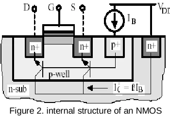
But what is important is that the body terminal voltage value should also be limited because pad lock or leakage current through device internal diodes will effect on the transistor function.
if the input voltage of the body (in the device NMOS) increases, internal bonds PN between the body and source and that of the drain and body source will become active and even activates the links (Figure 2). In addition unwanted BJT transistors may be activated and pad locking happen.
2
) (
2 GS th
ox n
D V V
l w C
612
Figure 1. the drain current with respect to body-source and gate - source voltage
Figure 2. internal structure of an NMOS
In DC analysis of transistor circuit , the drain current can be calculated via following equation regardless of any arrangement.
20
0 2 2
2lV V f V f
w C
ID ox GS TH SB (8)
Which the following equations are defined in: Saturation region
TH GS
DS V V
V (9)
Triode region VDS VGS VTH (10)
Cut-off region VGS VTH (11)
So the DC voltage of body - source terminal has a feature either in circuits(Bulk-Driven) or in circuits (Gate-Driven) and will change the operating point to the same extent .In Small-signal analysis of a device as body-driven or with gate input or observing small signal model of the amplifiers we will have the following equations .
Latch up:
2 2
mbs m m
SB
g g g
f V
(12)
( iD )( TH) mbs
s Th s
V ID
g
V B V V B
(13)
( iD )
m
GS Th
ID g
V V
(14)
2 2
TH
V
VSB f VSB
(15)
0.2
x
0.4
2
2
0.25
0.5
BS
613
Another weakness with the body input is its speed reduction relative to the moment the same device works with input gate frame (Philllip and Benjamin, 2003; Pease, 2000).
driven gate t driven
bulk
t
f
f
8
.
3
(17)
Comparison of methods
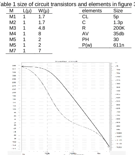
Figures 3, 4 and 5 are respectively the circuits with quite similar structure which their differences are: how to insert the input voltage to the circuit, how to bias and also kind of input transistor. The circuit K in the first floor is a PMOS differential double floor circuit that was used.
The second floor circuit is a low voltage amplification AB. a voltage source was used to bias the second floor circuit. We examine 3 parameters such as size ,phase margin and consumption power to compare the methods for achieving the voltage gain in 35 dB. Figure 3 shows the circuit with differential pair input in the body-driven layout.
Figure 3. the circuit with body-driven input
Table 1 size of circuit transistors and elements in figure 3
M L(µ) W(µ) M1 1 1.7 M2 1 1.7 M3 1 4.8 M4 1 8 M5 1 2 M5 1 2 M7 1 7
elements Size
CL 5p
C 1.3p
R 200K
AV 35db
PH 30
P(w) 611n
614
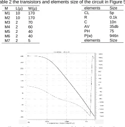
Figure 5. the proposed circuit which all devices are biased in sub-threshold region
Table 2 the transistors and elements size of the circuit in Figure 5
M L(µ) W(µ) M1 10 170 M2 10 170 M3 2 70 M4 2 60 M5 2 40 M6 2 40 M7 2 5
elements Size
CL 5p
R 0.1k
C 10n
AV 35db
PH 75
P(w) 946n elements Size
Figure 6. Frequency response of the circuit in Figure 5
It can be seen that in Comparison of phase margin and In comparison of power consumption two methods are perceived. The sub-threshold method has less consumption power in proportion other methods.
CONCULSION
In the paper after designing a double floor circuit by 2 methods which has been carried out through 0/6 V supply voltage; it was evident that even if all of them can be used in low supply voltage very well but depending on the overall goal everyone can be used. For example, if circuit design target is led to very low consumption power the sub-threshold technique is the most appropriate one However; its low frequency response still remains as before or if the objective of circuit design is with a suitable volume of bulk.
REFERENCES
Rosenfeld J, Kozak M. 2004. “A Bulk-Driven CMOS OTA with 68db DC Gain,” 11 th IEEE International conference.on circuit and System,ICECS 2004,dec.2004,pp.5-8.
Ramirez J. 1996. "Low Supply Voltage Ota Artitecture Using Floating Gate Transistors"IEEE Electrical and computer engineering.
Sing B. 2003. King Fahd university of petroleum and Minerals "Ultera-LowVoltage Operational amplifier".
Philllip E and Allen Benjamin J. 2003. Blalock scool of electrical and computer engineering Georgia institute of technology Atlanta"Low voltage analog circuits using standards Cmos technology".