IMPLEMENTATION OF DIGITAL QPSK
MODULATOR BY USING VHDL /
MATLAB
Teena Sakla*
Technocrats Institute of Technology Bhopal-462021 House No 685 Kumhar Mohalla Bairagarh Bhopal- 462030
(MP) India
Divya Jain
Technocrats Institute of Technology Bhopal-462021 (MP) India
Sandhya Gautam
Technocrats Institute of Technology Bhopal-462021 (MP) India
ABSTRACT
The modulators are the basic requirement of the communication systems they are designed to reduce the channel distortion & to use in RF communication hence many type of carrier modulation techniques has been already proposed according to channel properties & data rate of the system. Here we are proposing the FPGA based QPSK modulator with analog filters, the proposed system has many advantages over traditional QPSK modulators such as reduced cost, better stability, less complexity. The simulation of the system proves all the features mention above. We have designed the system using VHDL codes in Xilinx & analog filter simulation in Matlab. Three types of filters are investigated. The filters simulation results are compared and presented in this paper.Keywords: QPSK, VHDL, Wavelet Transform, Filters.
1.Introduction Modulation is very important block in communication system to transmit the data through channel without loss of data & to reduce size of antenna incase of wireless communication it is also important aspect for FDM. Because of these requirements many models are proposed to design a stable & low power modulator because the requirement of the sine wave as carrier most of the previously proposed models uses the analog circuitry for modulators but the stability of the analog system very much depends upon physical condition of the device as temperature, humidity etc. hence to make design robust & immune to physical conditions we are here proposing the FPGA based technique which not only improves the stability but also the power requirement of the system it also works on higher bit rate than the previously proposed analog systems. The proposed model involves a FPGA based 4X1 multiplexer, one clock & four delay blocks to produce four phases then the output is filtered by the analog filter to produce smooth sinusoidal wave at the output.
not include simulation of the high frequency RF blocks. The next step in these simulations is to provide a benchmark for the transceiver system performance by implementing a realistic RF transmission channel.
3. Proposed Model
All analogue or hybrid analogue/digital QPSK modulators work with phase shift carrier angle, as a key of modulation [8]. The phase signal is most important part in the modulator to acquire two discrete signals (Sine and Cosine) [17]. However, the NRZ format is essential for mapping I and Q. The analogue QPSK signal can be represented mathematically as in Equation (1) and I/Q are defined in Equations (2, 3):
QPSK (t) = I (t) cos (2π f c t) – Q (t) sin (2π f c t) (1.1) I =√2E/T cos [(2i-1) π/4] (1.2) Q=√2E/T sin [(2i-1) π/4] (1.3) These types of technique are not suitable for medical applications, which essential work with the input data in NRZ signal form at conventional modulators. The proposed QPSK VHDL modulator is programmed generate a carrier phase which acquires four discrete states (0, 90,180,270). Two separate streams in-phase ’I’, and quadrature phase Q for mapping the data for controlling the four phase different carriers interfaced to multiplexer.
The output is selected by multiplexer to provide a digital QPSK signal, which passes via a passive filter before a transmission (TX) to eliminate the high frequencies [9]. Fig.1 demonstrates the proposed VHDL modulator comparing to analogue modulator. The QPSK modulator consists of carrier source to produce a periodic pulse signal (carrier signal ), fed to a carrier phase shifter; which shift the input carrier into four
different phase signals (0°, 90°, 180°, 270°) interfaced to multiplexer While the data_in is fed to data mapping to generate I and Q signals to influence the four phase different carries. The output is selected by multiplexer which provides digital QPSK signal, this signal filtered with analog filter before transmitted to pass fundamental frequency and eliminates the higher frequencies associated with the square signal. The architecture block diagram of QPSK modulator is shown in Figure.
Figure 1. The block diagram for the proposed QPSK Modulator 4. Simulation Results
A. VHDL programming code simulation
The proposed modulator programmed with the VHDL language for modeling, design and analysis of the proposed QPSK modulator. The simulated result of this modulator is presented in Fig.6. This demonstrates the output signals waveforms indicating the transitions (180°, 270°) of the carrier signal influence by input data signal. The carrier frequency 5 MHz was generated from the local clock signal The data signal was reduced to 5KHz by a frequency divider then fed into a random PN sequence generator. The modulator is implemented and the generated VHDL “Behavioral” RTL of the QPSK modulator is illustrated in Fig. 4
Carri er
Module
4X1
Multiplexer
Module
Analog Filter
Data_ Map
Figure 2. Top level RTL schematic for QPSK Figure 3. RTL schematic for QPSK Modulator
B.VHDL Simulation results and discussion
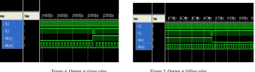
In this part of paper, we provide the simulation results for testing the VHDL code modulator. Figure 6 and figure 7 shows results at rising and falling edge of Input signal.clk_2 is carreir signal ,clk_3 is clock pulse to control the data rate of input signal,data_in is input signal and data_out is output signal.
Figure 4. Output at rising edge Figure 5. Output at falling edge
Pulse duration for clk_2 and clk_3 is 200ns and the pulse duration for data_out is 400ns.Following are the different possibilities of phase variation: 1. When data_in is 00 the phase of modulated signal is 0°.2. When data_in is 01 the phase of modulated signal is 90°.3. When data_in is 10 the phase of modulated signal is 180°.4. When data_in is 11 the phase of modulated signal is 270°.The signal passes as digital QPSK through the passive LPF for harmonics separation.
C. Filter Implementation and MATLAB simulation Results
In wireless transmission we cannot transmit the digital signal directly without harmonics separation. The output of the multiplier is producing a QPSK digital signal “square signal” form. It is essential to use a filter to complete the process for the modulator “off-chip”. We designed an analog passive filter for this purpose as it has zero power consumption. Two types of filters were investigated Low pass Filter (Wavelet LPF) and Band Pass Filter (second order Butterworth BPF) to eliminates the harmonics from the QPSK digital signal.
(I).Butterworth BPF simulation
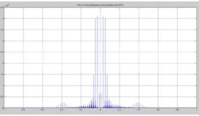
Figure 5. Butterworth Filter simulation Figure 6. The Wavelet Filter simulation with MATLAB
(II).Wavelet LPF simulation
Figure 3 shows the wavelet Energy spectrum for the result of the Haar transform or the frequency plot using wavelet packet frequency analysis. The peaks are formed by the filtered signal at the resolution of the level basis. By further reducing the time regions, all the frequency bands become compressed into a smaller time region. Multiple frequency bands become associated with a given time region.
5. Conclusion
========* Final Report *======== Final Results
RTL Top Level Output File Name: qpsk.ngr Top Level Output File Name: qpsk
Output Format: NGC Optimization Goal: Speed Keep Hierarchy: YES
Target Technology: Automotive 9500XL Macro Preserve: YES
XOR Preserve: YES Clock Enable: YES wysiwyg : NO Design Statistics # IOs: 4
Cell Usage: # BELS: 45 # AND2: 17 # AND3: 1 # GND: 1 # INV: 17 # OR2: 8 # XOR2: 1
# Flip-flops/Latches: 7 # FD: 5
# FDCE: 2 # IO Buffers: 4 # IBUF: 3 # OBUF: 1
===============================================================
wavelet (low pass) filter. It is clear from the table that wavelet filter gives the better results as compared to the others. In this thesis implementation of digital QPSK Modulator is done on XILINX 11.1i.The results are verified by test bench generated by the FPGA. Then the Analog filter is simulated by using MATLAB 7.5It can be concluded that the designed RTL model for QPSK Modulator is accurate and can work for real time application
TABLE1.Comparison of Simulation Results
Type of filter Data rate Carrier frequency Output bandwidth
Butterworth BPF 500 Kbps 5 MHz 2 MHz
Wavelet 500 Kbps 5 MHz 3 MHz
Butterworth LPF 500 Kbps 5 MHz 1 MHz
REFERENCES
[1] M.Kovac, J.kolouch “BPSK, QPSK MODULATOR SIMULATION MODUEL”2004
[2] E.Normark, Lei.Yang, C.Wakayama, P.Nikitin, R, Shi “VHDL –AMS Behavioral Modeling and simulation of a pi/4DQPSK transceiver system”
[3] T.J.Kazmierski, F.A.Hamid“Architectural and parametric optimization of low-pass RF anlog Filter in VHDL – AMS based high level synthsis”BMAS2004, San Jose,20-22 oct2004-2.
[4] Gihad Elamary ,Graeme. Chester, Jeffery Neasham” An Analysis of Wireless Inductive Coupling for High Data Rate Biomedical Telemetry Using a New VHDL n-PSK Modulator”
[5] K.Wise, D.Anderson, J.Hetke, R.Kipke, K.Najafi “Wireless implantable Microsystems High density Electronics interfaces to the nervous system”IEEE , Proceeding ,Vol.92,pp. 76-97, 2004.
[6] Ghazi Ben Hmida, Mhommed Dhieb, Hamadi Gharinai, Mounir Samet “ Transcutaneous Power and High Data Rata Transmission For Biomedical Implants” 2006 IEEE.
[7] S.Atluri, M.Ghovanloo “Digital of wideband power efficiency inductive wireless link for implantable biomedical using multiple carriers” Internal conference EMBS on neural engineering. IEEE, 2005
[8] A. M. El-Gabaly, B. R. Jackson and C. E. Saavedra, "An L-Band Direct-Digital QPSK Modulator in CMOS," IEEE International Symposium on Signals, Systems and Electronics, Montreal, Quebec, Canada, April 2007.
[9] B.Williams and Fred.J.Taylor, “Electronic Filter Design Handbook,” by the McGraw-Hill companies, vol. III, G. T. Rado and H. Suhl, Eds.USA: 2006, pp. 89–137,pp.165-239.
[10] G.C.Cardarilli, R. A.Del Re.RE, L.Simone Nicol, “Otimized QPSK Modulaator for DVB-S Applications,” ISCAS 2006 IEEE. [11] Douglas.L.Perry “VHDL Programming by Example”Mc.Grawh. USA: Academic 2002, pp. 842- 868
[12] www.altera.com/literature/univ/upds.pdf.(UP2 edicational board datasheet).
[13] Roger.Lipsett,Carl.Schaefer, Cary.Ussery “VHDL Hardware Description and design” pp842-868 [14] H.Bochnick,W.Anheier “FIR filter design using Verilog and VHDL”.Italy April.16-26.1993
[15] http://ieeexplore.ieee.org/iel5/7180/19335/00893288.pdf (“IEEE standred VHDL Language Reference Manual” [16] http://www.mathworks.co.uk/support/. (Matlab / Simulink sources)