Abstract— The purpose of this paper is to design low power and area efficient ALU using GDI technique. Main sub modules of ALU are adder, logical unit, comparator ,one’s complement, multiplexer. This work evaluates and compares the performance & optimized area of ALU with conventional CMOS style &GDI technique the simulations are performed by using cadence EDA tool in 180 nm technology. At first by using cadence virtuoso tool the circuits are designed &simulated with CMOS technique and then with GDI technique. by comparing two designs GDI&CMOS style then GDI is an advantage of less power and less area.
.
Index Terms—Adder, ALU, Comparator, GDI, Logical unit,
Low power, one’s complement, multiplexer.
I. INTRODUCTION
Recently , the industries are demand for low power, less area and high speed for designing the circuits. With improvement in technology and the enlargement of embedded system used electronic devices such as mobile, laptops, TV applications, power consumption, which is one of the limits in both high & low performance system, has become a primary focus in VLSI digital design.
In this paper the adder was based on regular CMOS structure (pull-up and pull-down network) [1].Disadvantage of this paper is but the uses a number of transistors results in high input loads, more power consumption and larger silicon area.
Morgenshtein has proposed basic GDI cell [2].By using this GDI cell we design ALU.
In digital system design processor is main part of the system. And an ALU is one of the main components of a micro-processor. CPU works as a brain to any system & and ALU works as a brain to CPU. So it’s a brain of computer’s brain. They consists of fast dynamic logic circuits and have
Manuscript received Oct , 2015
D.VIGNESHWARI, ECE department,JNTU University,Sridevi women’s engineering college, Hyderabad, India,9491370538.
K.SIVA NAGI REDDY, ECE Department JNTU University,Sridevi
women’s engineering College, Hyderabade.
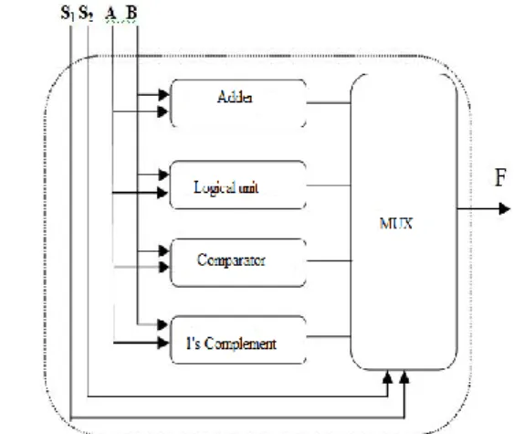
carefully optimized structures. Of total power consumption in any processor, CPU accounts a significant portion of it. Therefore , this motivate us strongly for a energy-efficient ALU designs that satisfy the high-performance requirements, while reducing power dissipation. ALU is a combinational circuit that performs arithmetic and logical operations e.g. A [0:3] & B [0:3] for 4 bits. Arithmetic operations are basic functions and necessary for any low power, high speed application digital signal processing, image processing, microprocessor. The internal structure of a ALU is shown in Fig.1.
Fig. 1: Internal structure of ALU
The rest of paper is organized as follows Section II describes
description of ALU. Section III consisting of designing of various ALU components such as comparator, adder, subtractor etc. using conventional CMOS..section IV presents the ALU using GDI technique Section V describes simulation result and analysis. At last conclusion is made in section VI.
II. DESCRIPTIONOFARITHMETICLOGICAL UNIT
In central processing unit(CPU) arithmetic logical unit (ALU) is a main component. it does all arithmetic logical operations and logical operations. The ALU is divided into the arithmetic unit (AU) and the logic unit (LU).
Design of Low Power ALU using GDI Technique
A. ARITHMETIC UNIT
Arithmetical operations are performed by using AU. arithmetical operations are addition, subtraction, multiplication etc .in this project . Fast and efficient adders in arithmetic logic unit will aid in the design of low power. Different adders are design in past to reduce the power , area and increase the speed.
B. LOGICAL UNIT
ALU can perform different logical operations that are AND, OR, NOT,NAND,NOR, EXOR, EXNOR etc. these logical operations are performed by using logical unit. by using mux particular logic operation to be performed.
C. COMPARATOR
The comparator is a very useful and basic arithmetic component of digital system. comparator compare the input values and produce the three out puts these are equal(A=B) less than condition(A<B), greater than (A>B)[3].when two inputs A,B are same values then it produces ‘e’ output ,if A value is higher than B value the output is ‘g’ else it produces out put as ‘l’.
D. ONE’S COMPLEMENT
By using one’s complement we can perform the inversion operation of the input. One’s complement perform by using NOT gate. NOT gate works like this if 1 is input then out put is 0 else output is 1.
E. MULTIPLEXER
Multiplexer is a combinational circuit that select several digital or analog input signal and forward the selected input into a single output line. Multiplexer is also called as data selector.in this project we use 4:1 mux [5].Sub modules are selected by multiplexer.
III ALU COMPONENTS DESIGN BY USING CMOS
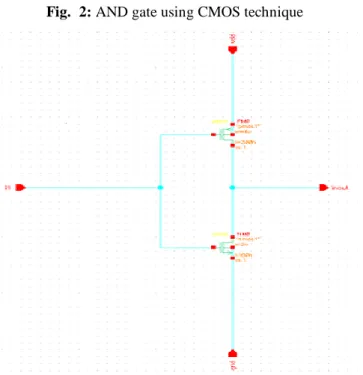
By using CMOS (complementary metal oxide semiconductor) technique The various components are designed. Figure shows the schematic design of various components such as ADDER, COMPARATOR, 1’S COMPLEMENT, LOGICAL GATES. The fig 2 shows the and gate using CMOS technique .this design uses 6 transistor.
Fig. 2: AND gate using CMOS technique
Fig. 3: Inverter using CMOS
The above figure 3 shows the CMOS inverter.it design by using PMOS and NMOS transistor.
Mostly all other circuits are design by using this three circuts AND,OR,NOT
.
IV PROPOSED GDI TECHNIQUE ALU
Morgenshtein has proposed basic GDI cell[4].The GDI cell fig 5 is shown in below.GDI cell design by using one PMOS,one NMOS transistor.It is same as CMOS inverter but only differences is two
1) First onesis it having three inputs pins,these are G,P,N and one out pin is out
1.Input pin G is common gate of PMOS and NMOS. 2.Input pin P is input to the source/drain of PMOS. 3.Input pin N is input to the source/drain of NMOS. 2) Bulks of NMOS and PMOS are connected to N or P (re- spectively), so it can be arbitrarily biased in contrast to CMOS inverter
Fig. 5 : GDI cell
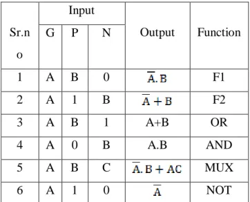
The basic GDI cell performs the below functions [6].the table is shown in below table I
I: GDI cell functions
Sr.n
o
Input
Output
Function
G
P
N
1
A
B
0
F1
2
A
1
B
F2
3
A
B
1
A+B
OR
4
A
0
B
A.B
AND
5
A
B
C
MUX
6
A
1
0
NOT
4 bit Adder circuit is design by using full adder,this 1-bit full adder [7]design by using GDI technique is shown in below fig 6.It requires a less number oftransistors compare to CMOS design
V SIMULATIONS AND RESULTS
This section describes the proposed ALU is design using GDI technique fig 7 in virtuoso tool on 180nm technology. the simulated out puts of proposed designs output are shown in figure 8.
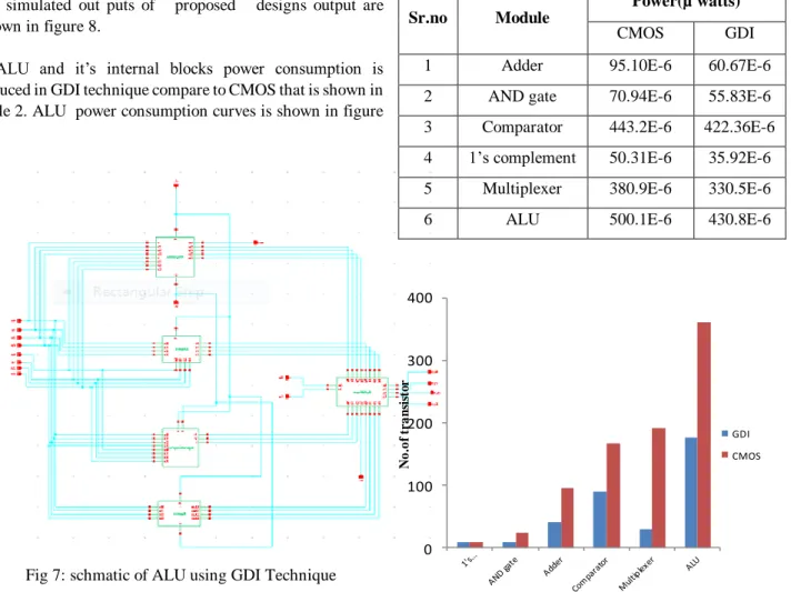
ALU and it’s internal blocks power consumption is reduced in GDI technique compare to CMOS that is shown in table 2. ALU power consumption curves is shown in figure 9.
Fig 7: schmatic of ALU using GDI Technique
Fig 8: Wave Forms of B it ALU Using GDI
II Power consumption of ALU and it internal blocks
Sr.no Module
Power(µ watts)
CMOS GDI
1 Adder 95.10E-6 60.67E-6
2 AND gate 70.94E-6 55.83E-6
3 Comparator 443.2E-6 422.36E-6 4 1’s complement 50.31E-6 35.92E-6 5 Multiplexer 380.9E-6 330.5E-6
6 ALU 500.1E-6 430.8E-6
Fig. 9: Graph describing a comparison of no.of transistors in
both CMOS and GDI.
ALU design by using proposed GDI technique uses a less number of transistor so area is optimized. if use less no.of transistor then speed is also increase then operating time is reduced. so proposed GDI ALU uses a low power and less no.of transistor, design complexity. figure 9 shows the number of transistor are used for designing ALU and internal blocks, in that GDI technique uses a less number of transistors.
V CONCLUSION
In this paper, conventional CMOS technique for the designing of ALU is discussed first. A low power and area optimizing technique is introduced and the components with this technique are implemented. Later the comparison between the number of transistor used in CMOS and GDI design of ALU is done. And in the results is shows that this GDI design is reduces the power and the number of transistor and hence optimize the area of ALU as well increase its working speed. 0 100 200 300 400 N o .o f tr a n si st or
Diffe rent blocks
GDI CMOS
REFERENCE
[1] R. Shalem, E. John, and L.K. John, proposed a conventional CMOS full adder consisting of 28 transistors [2] Arun Prakash Singh, Rohit Kumar, ―Implementation of 1-bit Full Adder using Gate Diffusion Input (GDI) cell ‖, International Journal of Electronics and Computer Science Engineering, ISSN- 2277-1956/V1N2-333-342
[3] Vijaya Shekhawat,Tripati,Krishna Gopal Sharma,-2 bit magnitude comparator using GDI Technique
[4] Arkadiy Morgenshtein, Alexander Fish, and Israel A. Wagner, ―Gate-Diffusion Input (GDI): A Power-Efficient Method for Digital Combinatorial Circuits‖, IEEE Transactions On Very Large Scale Integration (VLSI) Systems, Vol. 10, No. 5, October 2002
[5] Vaibhav Neema, Pratibha Gupta, ―Design Strategy for Barrel Shifter Using Mux at 180nm Technology Node ‖, International Journal of Science and Modern Engineering (IJISME), ISSN: 2319-6386, Volume-1, Issue-8, July 2013 [6] Shrivastava, A.; Kannan, D.; Bhardwaj, S. Vrudhula, Reducing functional unit power consumption and its variation using leakage sensors, IEEE transactions on very large scale integration (VLSI) systems, vol. 18, no. 6, pp.988-997, June 2010
[7] Dan Wang, Maofeng Yang, Wu Cheng, Xuguang Guan, Zhangming Zhu, Yintang Yang, ―Novel Low Power Full Adder Cells in 180nm CMOS Technology‖, ICIEA 2009, 978-1-4244- 2800-7/09/$25.00 ©2009 IEEE
D VIGNESHWARI, PG scholar, Dept of ECE ,Sridevi
women’s engineering college ,Hyderabad,TS, India,
K SIVA NAGI REDDY, Associate professor in Sridevi
women’s engineering college. He completed his M.E and pursuing his Ph.D His research interests in VLSI and Image processing.