Vol. 47, No. 1, Spring 2015, pp. 39- 45 )AIJ-EEE)
٭
Corresponding Author, Email: [email protected]
Filtering Power Divider/Combiner Based on Half Mode
Substrate Integrated Waveguide (HMSIW) Technology
for High Power Applications
A. R. Moznebi
1and K. Afrooz
2*1-MSc Student, Department of Electrical Engineering, Shahid Bahonar University of Kerman, Kerman, Iran 2-Assistant Professor, Department of Electrical Engineering, Shahid Bahonar University of Kerman, Kerman, Iran
ABSTRACT
A filtering power divider/power combiner based on half mode substrate integrated waveguide technology
for high power applications is proposed. This design includes one half mode substrate integrated waveguide
cavity, one matched load, and four sections of quarter-wavelength transmission lines. The high isolation
between output ports is obtained by combining the half mode substrate integrated waveguide cavity and
microstrip network (one matched load and four sections of quarter-wavelength transmission lines). This
structure utilizes for high power applications because of the matched load is connected to ground. The design
is fabricated and tested by network analyzer. A good agreement between the simulated and measured results
is observed. The measured results show that for a return loss of 15 dB, the bandwidth is from 5.15 to 5.35
GHz (IEEE 802.11a wireless local area network (WLAN) standard) and over this whole bandwidth, the
output return loss and isolation between output ports are better than 14.5 dB and 17.5 dB, respectively. Also,
the measured insertion loss is
4.4 0.1dB.
KEYWORDS
1- INTRODUCTION
In millimeter-wave and microwave circuits, power dividers (PDs)/ power combiners (PCs) are one of the common and essential components. The traditional waveguide PD has the obstacles such as large size and integration with planar structures [1]. Recently, the substrate integrated waveguide (SIW) is introduced [2,3]. This structure is formed by two rows of metallic via holes in a planar substrate (as shown in Fig. 1) and has the advantages of low cost, low loss, high Q-factor, and most importantly small size and integration capabilities with planar circuits [4]. The
half mode substrate integrated
waveguide
(HMSIW) has the all of them and also it hasa smaller size than the SIW [5].
Via hole
d s
H
Fig.1. Configuration of a SIW structure.
The output matching and isolation are necessary to improve circuit performance. The Wilkinson PD [6] has been widely used in microwave circuits and systems because of good bandwidth, high isolation, low return loss and low insertion loss [7-9]. In this circuit, the resistors generate the heat dissipation due to they are not connected to ground. Moreover, the disruption in result is occurring due to the coupling output ports with each other in high frequency applications. Therefore, the Wilkinson PD utilizes for low power applications. As opposed to, the Gysel PD [10] is introduced for high power applications since the grounded resistors and heat transfer to ground.
Several SIW/HMSIW power dividers have been investigated [11-15]. Periodic butterfly radial slots power divider with enhanced out-of-band rejection had relatively large amplitude imbalance [11]. A broadband SIW T-junction with an arbitrary power-dividing ratio was presented [12]. This circuit had relatively large volume. SIW Y-junction power divider had comparatively large insertion loss [13]. In addition, these designs [11-13] did not have isolation between output ports. A compact SIW Wilkinson power divider and a broadband HMSIW Wilkinson power divider were introduced [14,15]. Due to the attached resistor, these structures were not proper for high power applications.
In this paper, a filtering PD/PC with high isolation for high power applications based on HMSIW and microstrip
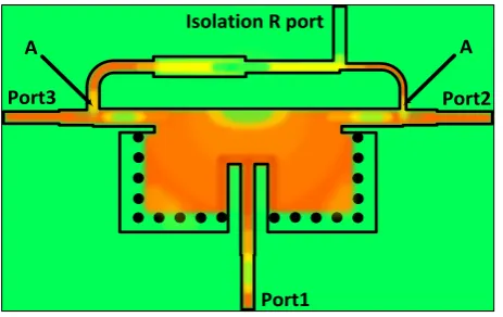
transmission lines is introduced. This PD/PC consists of one HMSIW cavity, one matched load, and four sections of quarter-wavelength transmission lines. The high isolation and high power applications is obtained because of the part of the Gysel PD is connected to the HMSIW cavity. Fig. 2 shows the building block of the proposed structure.
Microstrip Network
HMSIW cavity
Port 1
Port 3 Port 2
Fig.2. Building block of the proposed structure.
In this structure, the excited mode is TE101 mode. For
design, an EM simulator and Rogers RO4003C substrate are used. This circuit is fabricated and the measured results are sampled by network analyzer.
A good agreement between the simulated and measured results is seen. For a return loss of 15 dB, the measured bandwidth is from 5.15 to 5.35 GHz (IEEE 802.11a WLAN standard). Fig. 3 displays the schematic of the proposed structure.
Port1
Port3 Port2
Isolation R port
`
W L Wg2
Wt2 Lt3
Lt1
Wt1
Lg1
Wg1
Wt3
Lg2
Lt2
Z1 Z2 Z3
Z4
Z0
Z0 Z0
Z0
Lt5
s d
Lt4
Fig.3. Schematic of the proposed structure.
2- GYSEL POWER DIVIDER
Port 1
Port 2
Port 3
R
R
Fig.4. Configuration of the conventional Gysel PD.
This PD has the five ports and five branch-line sections with the characteristic impedances of Z2=Z0=50,
0
1 2
Z Z , and 0
3
2
Z
Z . In this section, the even and
odd mode analyses are used to obtain the value of the characteristic impedances.
2-1- EVEN MODE
In the even mode, the potential at port 2 and port 3 should be of equal magnitude and phase. The equivalent circuit of this case is illustrated in Fig. 5.
R
R
Fig.5. Equivalent even mode circuit of the conventional Gysel PD.
The simplified circuit of the Fig. 5 is shown in Fig. 6.
Fig.6. Simplified circuit of the Fig. 5.
As a result, the value of Z1 is selected equal toZ0 2.
2-2- ODD MODE
R
R
Fig.7. Equivalent odd mode circuit of the conventional Gysel PD.
In the odd mode, port 2 and port 3 are excited out of phase by 180 degrees. The equivalent circuit of this case is illustrated in Fig. 7. The simplified circuit of the Fig. 7 is shown in Fig. 8.
R
Fig.8. Simplified circuit of the Fig. 7.
In this case, R=50 and Z2=50. Moreover, the value of Z3
is does not care. The lowest impedance of Z3 is equal
maximum bandwidth. A Gysel PD is designed at the center frequency of 5.2 GHz and simulated by EM simulator. Fig. 9 depicts the results of this PD. This circuit has not a proper bandpass-filtering response.
Fig.9. Results of the conventional Gysel PD.
3- DESIGN AND ANALYSIS 3-1- DESIGN PROCEDURE
In this structure, the excited mode is TE101 mode. For
SIW cavity, the cutoff frequency is obtained by [16]:
2 3 4 5 6 7 8 9 10
-60 -50 -40 -30 -20 -10 0
Frequency (GHz)
S
P
a
ra
m
e
te
r
(d
B
)
S11
S
12
S13
S23
S22
S
2 2
0
2
m n
eff eff r r
c
m
n
f
W
L
(1)In (1), m and n are the mode indexes, c is the velocity of light in the free space,
r is the relative permittivity of the substrate, ris the relative permeability of the substrate, Leff refers to the equivalent length, and Weffrefers to the equivalent width which they are equal to [17]:
2 2
1.08.
0.1.
eff
d
d
W
W
s
W
, (2)2 2
1
1
1.08.
0.1.
eff
d
d
L
L
s
L
(3)In (2), d refers to the diameter of the vias, s is their longitudinal spacing, W displays the width of the SIW cavity, and L1 shows the length of the SIW cavity. For
HMSIW cavity, the length of the SIW cavity is halved. In this structure, The TM modes cannot guided because of the vias are separated by the dielectric gap [18] which for the better performance of the circuit, d and s are limited as follow [19]:
2
s
d
(4)In this paper, the center frequency is 5.25 GHz. Table I exhibits the dimensions of the HMSIW PD/PC shown in Fig. 3. In this Table, other dimensions except W, L, s, and d is performed with optimization of proposed structure using EM simulator to get low insertion loss, good return loss in all port and good isolation between output ports. For receive high isolation, part of the Gysel PD is joined to HMSIW cavity. The used Gysel PD is introduced in [20]. In this design, Z0=Z1=Z3=50,
0 2
2
Z
Z , and Z4Z0 2 where all the transmission
lines are a quarter-wavelength long.
TABLE I
DIMENSIONS OF THE PROPOSED STRUCTURE (UNITS:MM)
5.42 Lt2
19.74 W
.8 Lt3
1.27 Wt1
5.17 Lt4
1.65 Wt2
2.54 Lt5
1.42 Wt3
6.35 Lg1
3.65 Wg1
3.3 Lg2
2.22 Wg2
1.9 s
10.16 L
0.95 d
8.5 Lt1
3-2- EVEN AND ODD MODE ANALYSIS
In the even mode, the microstrip network is open circuit (ponit A) and the scattering parameters in the even mode are the scattering parameters of the HMSIW cavity in the even mode. The current distribution of the HMSIW PD/PC in the even mode shown in Fig. 10.
Fig. 10. Current distribution of the HMSIW PD/PC in even mode.
Fig. 11 indicates the current distribution of the HMSIW PD/PC in the odd mode. In this case, the HMSIW cavity is not excited and point A is open circuit. Therefore, the scattering parameters in the odd mode are the scattering parameters of the microstrip network in the odd mode.
`
Fig.11. Current distribution of the HMSIW PD/PC in odd mode.
4- SIMULATED AND MEASURED RESULTS
output return loss and isolation between output ports are better than 14.5 dB and 17.5 dB, respectively. Also, the measured insertion loss is 4.4 0.1 dB and the amplitude imbalance and phase imbalance are less than 0.26
dB
and 3.5 , respectively.Port 1
Port 2 Port 3
Isolation R port
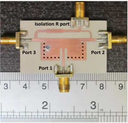
Fig.12. Photograph of the proposed structure.
Fig. 13 illustrates S11 and S12, Fig. 14 shows S22 and
S
23, and Fig. 15 and Fig. 16 indicate the simulated and measured results of the amplitude imbalance and phase imbalance, respectively. The slightly difference between the simulated and measured results may be introduced by the tolerances of dielectric constant and the insertion loss of SMA connectors. In the end, these results introduce a circuit with low cost, low loss, high Q-factor, high selectivity, compact size and integration capabilities with planar circuits. Moreover, this design is proper for high power applications.Fig.13. Simulated and measured S11, S12, and S13 of the
HMSIW PD/PC.
Fig.14. Simulated and measured S23, S22, and S33 of the
HMSIW PD/PC.
Fig.15. Simulated and measured amplitude imbalance of the HMSIW PD/PC.
Fig.16. Simulated and measured phase imbalance of the HMSIW PD/PC.
In Table II, a comparison between this work and the other previously works is summarized.
2 3 4 5 6 7 8 9 10
-40 -35 -30 -25 -20 -15 -10 -5 0 Frequency (GHz) S P a ra m e te r (d B ) S
11 Measured S
11 Simulated S
12 Measured S
12 Simulated S
13 Measured S
13 Simulated
2 3 4 5 6 7 8 9 10
-40 -35 -30 -25 -20 -15 -10 -5 0 Frequency (GHz) S P a ra m e te r (d B ) S
23 Measured S
23 Simulated S
22 Measured S
22 Simulated S
33 Measured S
33 Simulated
5.1 5.15 5.2 5.25 5.3 5.35 5.4
0.16 0.18 0.2 0.22 0.24 0.26 0.28 Frequency (GHz) A m p lit u d e I m b a la n c e ( d B ) Simulated Measured
5.1 5.15 5.2 5.25 5.3 5.35 5.4
TABLE II
COMPARISON WITH OTHER PREVIOUSLY WORKS
Isolation IL
(dB) 15 dB
Return loss
FBW (%) Size
(
g2) ReferenceNo <1 12
0.88 4.08 [21]
Yes <2
1.6 1.72 2.57
[22]
Yes <1.5 3.8
0.61 1.14 This work
5- CONCLUSION
In this paper, a filtering PD/PC with high isolation for high power applications based on HMSIW has been designed. It can be utilized in microwave and millimeter-wave systems. Also, this circuit has a compact size of
2
34.57 18.55 mm . This model has the excellences of integrate with planar circuits and small size than traditional waveguide PDs and it has the benefit of use for high power applications than SIW/HMSIW Wilkinson PDs.
REFRENCES
[1] Z. Hao, W. Hong, H. Li, H. Zhang, and K. Wu, “Multiway broadband substrate integrated waveguide (SIW) power divider”, In IEEE Antennas and Propagation Society Int. Symp., pp. 639-642, 2005.
[2] H. Uchimura, T. Takenoshita, and M. Fujii, “Development of a “laminated waveguide””, IEEE Trans. Microw. Theory Tech., vol. 46, no. 12, pp. 2438-2443, November, 1998.
[3] L. Yan, W. Hong, K. Wu, and T. J. Cui, “Investigations on the propagation characteristics of the substrate integrated waveguide based on the method of lines”, IET Microw. Antennas Prop., vol. 152, no. 1, pp. 35-42, February, 2005.
[4] M. Bozzi, A. Georgiadis, and K. Wu, “Review of substrate-integrated waveguide circuits and antennas”, IET Microw. Antennas Prop., vol. 5, no. 8, pp. 909-920, June, 2011.
[5] W. Hong, B. Liu, Y. Wang, Q. Lai, H. Tang, X. X. Yin, Y. D. Dong, Y. Zhang, and K. Wu, “Half mode substrate integrated waveguide: A new guided wave structure for microwave and millimeter wave application”, In Infrared Millimeter Waves and 14th International Conference on Teraherz Electronics, Shanghai, pp. 219-219, 2006.
[6] E. J. Wilkinson, “An N-way hybrid power divider”, IRE Trans. Microw. Theory Tech., vol. 8, no. 1, pp. 116-118, January, 1960.
[7] K. K. M. Cheng, and P. W. Li, “novel power-divider design with unequal power-dividing ratio and simple layout”, IEEE Trans. Microw. Theory Tech., vol. 57, no. 6, pp. 1589-1594, May, 2009.
[8] H. R. Ahn, and I. Wolff, “Ahn, H. R., & Wolff, I. (2001). General design equations, small-sized impedance transformers, and their application to small-sized three-port 3-dB power dividers”, IEEE Trans. Microw. Theory Tech., vol. 49, no. 7, pp. 1277-1288, July, 2001.
[9] M. J. Park, and B. Lee, “A dual-band Wilkinson power divider”, IEEE Microw. Wirel. Compon. Lett., Vol. 18, no. 2, pp. 85-87, February, 2008.
[10] U. H. Gysel, “A new N-way power divider/combiner suitable for high-power applications”, In IEEE Microw. Symposium, Palo Alton, CA, pp. 116-118, 1975.
[11] S. Y. Chen, D. S. Zhang, and Y. T. Yu, “Wideband SIW power divider with improved out-of-band rejection”, Electron. Lett., vol. 49, no. 15, pp. 943-944, July, 2013.
[12] T. Li, and W. Dou, “Broadband substrate-integrated waveguide T-junction with arbitrary power-dividing ratio”, Electron. Lett., vol. 51, no. 3, pp. 259-260, February, 2015.
[13] X. Zou, C. M. Tong, and D. W. Yu, “Y-junction power divider based on substrate integrated waveguide”, Electron. Lett., vol. 47, no. 25, pp. 1375-1376, December, 2011.
[14] N. Smith, and R. Abhari, “Compact substrate integrated waveguide Wilkinson power dividers”, In IEEE Antennas and Propagation Society Int. Symp., Charleston, SC, pp. 1-4, 2009.
[15] Z. Y. Zhang, and K. Wu, “Broadband half-mode substrate integrated waveguide (HMSIW) Wilkinson power divider”, In IEEE Microw. Symposium Digest, Atlanta, GA, pp. 879-882, 2008.
[16] D. M. Pozar, Microwave Engineering. Wiley, 2011.
[17] F. Xu, and K. Wu, “Guided-wave and leakage characteristics of substrate integrated waveguide”, IEEE Trans. Microw. Theory Tech., vol. 53, no. 1, pp. 66-73, January, 2005.
[18] J. E. Rayas-Sánchez, and V. Gutierrez-Ayala, “A general EM-based design procedure for single-layer substrate integrated waveguide interconnects with microstrip transitions”, In IEEE Microw. Symposium Digest, Atlanta, GA, pp. 983-986, 2008.
In Telecommunications in Modern Satellite, Cable and Broadcasting Service, pp. P-III, 2003.
[20] A. Abbosh, and B. Henin, “Planar wideband inphase power divider/combiner using modified Gysel structure”, IET Microw. Antennas Prop., Vol. 7, no. 10, pp. 783-787, July, 2013.
[21] J. N. Hui, W. J. Feng, and W. Q. Che, “Balun bandpass filter based on multilayer substrate integrated waveguide power divider”, Electron. Lett., vol. 48, no. 10, pp. 571-573, May, 2012.
![TABLE II [7]](https://thumb-us.123doks.com/thumbv2/123dok_us/17741.2001813/6.595.63.281.112.240/table-ii.webp)