Single DV-DXCCII Based Voltage Controlled First Order
All-Pass Filter with Inverting and Non-Inverting Responses
B. Chaturvedi* and J. Mohan*(C.A.)
Abstract: In this paper, a new voltage controlled first order all-pass filter is presented. The
proposed circuit employs a single Differential Voltage Dual-X second generation Current Conveyor (DV-DXCCII), a NMOS (n-type Metal Oxide Semiconductor) transistor operated in the triode region as an active resistor and a grounded capacitor. The proposed all-pass filter provides both inverting and non inverting voltage-mode outputs simultaneously from the same configuration without any matching constraint. Non-ideal analysis along with sensitivity analysis is investigated. The proposed circuit has low active and passive sensitivities. The Monte Carlo analysis is also done for showing good sensitivity performances of the proposed circuit. In addition, to utilize the feature of cascadability, an application of higher order filter is also given. Moreover, the use of grounded capacitor makes the proposed circuit particularly attractive for Integrated Circuit (IC) implementation point of view. The theoretical results are validated through PSPICE simulations with TSMC 0.18 µm Complementary Metal Oxide Semiconductor (CMOS) process parameters.
Keywords: All-Pass Filter, Dual-X Current Conveyor, First Order, Voltage-Mode.
1 Introduction1
All-pass filters are widely used to shift the phase of the signal while keeping its amplitude constant over the desired frequency range. Thus all-pass filters can correct the undesired change in phase during analog filtering operations. The literature survey shows that several first-order all-pass filter (APF) circuits using different types of active building blocks such as second generation current-controlled current conveyor (CCCII) [1], differential voltage current conveyor (DVCC) [2- 4, 7, 8, 10], inverting voltage buffer (IVB) [9], operational transconductance amplifier (OTA) [5, 6, 8, 11], second generation current conveyor (CCII) [13, 17, 25], third generation current conveyor (CCIII) [14], differential difference current conveyor (DDCC) [15, 29], dual-X second generation current conveyor (DXCCII) [19, 23], current conveyors (CC) [16], current differencing buffered amplifier (CDBA) [17], fully differential second generation current conveyor (FDCCII) [20, 30], universal voltage conveyor (UVC) [6, 22], voltage differencing inverting buffered amplifier (VDIBA) [24], Extra-X current controlled conveyor (EX-CCCII) [26],
Iranian Journal of Electrical & Electronic Engineering, 2015. Paper first received 23 Mar. 2015 and in revised form 30 Sep. 2015. * The Authors are with the Department of Electronics and Communication Engineering, Jaypee Institute of Information Technology, Noida-201304 (India).
E-mails: [email protected] and [email protected].
differential difference dual-X second generation current conveyor (DD-DXCCII) [27], current controlled conveyor transconductance amplifier (CCCTA) [28] have been reported. A study of some recently published first-order voltage mode all-pass filters based on single active element is presented in this section [11-30]. The filter circuits presented in [11-20, 22, 23, 25, 29, 30] require more than one passive components to realize first-order APF and few of them also require matching condition [11-14, 17, 19, 22, 25, 29]. However, the circuits presented in [11, 15, 16, 18, 20, 23, 30] are based on one active element and two passive components. The reported circuits do not require any matching condition. In order to add the tunability in the existing circuits, a resistorless realization can be implemented by replacing the resistor with a MOSFET based voltage controlled resistor. Recently, the resistorless voltage mode first-order all-pass filter based on single active element was presented in [21, 24, 26-28]. However, the circuit presented in [24, 27, 28] employs floating capacitor. It is well known fact that a floating capacitor can be realized as double poly layer. However the grounded IC capacitors have less parasitics compared to floating counterparts, which is significant from the performance point of view [33]. Table 1 presents a comparison of some of the reported first order voltage-mode all-pass filter based on single active element.
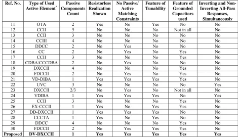
Table 1 Comparison study of the existing single active element based voltage-mode all pass filter circuits with the proposed circuit. Ref. No. Type of Used
Active Element*
Passive Components
Count
Resistorless Realization
Shown
No Passive/ Active Matching Constraints
Feature of Tunability
Feature of Grounded Capacitors
used
Inverting and Non-Inverting All-Pass
Responses, Simultaneously
11 OTA 2 Yes No Yes No No
12 CCII 5 No No No Not in all No
13 CCII 3 No No No No No
14 CCIII 4 No No No No No
15 DDCC 2 No Yes No No No
16 CC 2 No Yes No Yes No
17 CCII 3 No No No Yes No
18 CDBA/CCCDBA 2 No Yes No No No
19 DXCCII 4 No No No Yes No
20 FDCCII 2 No Yes No Yes No
21 VD-DIBA 1 Yes Yes Yes Yes No
22 UVC 3 No No No No Yes
23 DXCCII 2/3 No Yes No Not in all No
24 VDIBA 1 Yes Yes Yes No Yes
25 CCII 3 No No No Yes No
26 EX-CCCII 1 Yes No Yes Yes No
27 DD-DXCCII 1 Yes Yes Yes No No
28 CCCTA 1 Yes No Yes No No
29 DDCC 4 No No No Yes No
30 FDCCII 2 No Yes Yes Yes No
Proposed DV-DXCCII 1 Yes Yes Yes Yes Yes
* Abbreviations: OTA: Operational Transconductance Amplifier, CCII: Second Generation Current Conveyor, CCIII: Third Generation Current Conveyor, DDCC: Differential Difference Current Conveyor, CC: Current Conveyor, CDBA: Current Differencing Buffered Amplifier, CCCDBA: Current Controlled Current Differencing Buffered Amplifier, DXCCII: Dual-X Second Generation Current Conveyor, FDCCII: Fully Differential Second Generation Current Conveyor, VD-DIBA: Voltage Differencing Differential Input Buffered Amplifier, UVC: Universal Voltage Conveyor, VDIBA: Voltage Differencing Inverting Buffered Amplifier, EX-CCCII: Extra-X Current Controlled Conveyer, DD-DXCCII: Differential Difference Dual-X Second Generation Current Conveyor, CCCTA: Current Controlled Conveyor Transconductance Amplifier, DV-DXCCII: Differential Voltage Dual-X Second Generation Current Conveyor.
This paper presents a new voltage controlled first order all-pass filter (VC-APF) based on differential voltage dual-X second generation current conveyor (DV-DXCCII). The proposed circuit employs a single DV-DXCCII, a NMOS transistor operated in the triode region and a grounded capacitor. The proposed circuit provides both inverting and non-inverting all-pass responses simultaneously at two different terminals without any matching constraint. The feature of low output impedance at the one output terminal is also explored by realizing an nth order VC-APF. It can be
noticed from the comparison Table 1 that none of the reported circuits realized a tunable first order voltage mode all-pass filter with both inverting and non-inverting all-pass responses simultaneously from the same circuit by employing a single active element, an active resistor and a grounded capacitor.
2 Proposed Circuit
DV-DXCCII is a six terminal analogue building block which is characterized by the following port relations
⎥ ⎥ ⎥ ⎥
⎦ ⎤
⎢ ⎢ ⎢ ⎢
⎣ ⎡
⎥ ⎥ ⎥ ⎥ ⎥ ⎥ ⎥ ⎥
⎦ ⎤
⎢ ⎢ ⎢ ⎢ ⎢ ⎢ ⎢ ⎢
⎣ ⎡
− −
− =
⎥ ⎥ ⎥ ⎥ ⎥ ⎥ ⎥ ⎥
⎦ ⎤
⎢ ⎢ ⎢ ⎢ ⎢ ⎢ ⎢ ⎢
⎣ ⎡
− +
− + − +
X X Y Y
z z X X Y Y
I I V V
I I V V I I
2 1 2
1
1 0 0 0
0 1 0 0
0 0 1 1
0 0 1 1
0 0 0 0
0 0 0 0
(1)
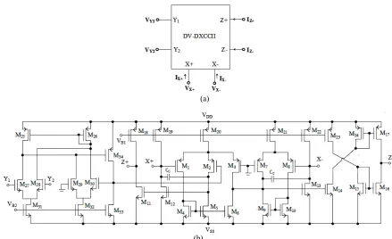
DV-DXCCII combines the advantages of the DVCC [31] and DXCCII [32]. The symbol and the CMOS implementation of DV-DXCCII is shown in Fig. 1(a) and Fig. 1(b), respectively. The CMOS implementation of Fig. 1(b) comprises of DVCC (M25–M34) with
unemployed Z-stages and DXCCII (M1–M24). In the
CMOS implementation of DV-DXCCII, the X-terminal (gate of M30) of DVCC drives the Y-terminal (gate of
M2) of the DXCCII.
The Z+ and Z- stages are realized from the drain of M11 and M16 transistors. The DV-DXCCII has two high
impedance input terminals (Y1 and Y2), two low
impedance terminals (X+ and X-) and two high impedance output terminals (Z+ and Z-).
(a)
(b)
Fig. 1 (a) Symbol of DV-DXCCII (b) CMOS implementation of DV-DXCCII.
The proposed voltage controlled first-order all-pass filter (VC-APF) is shown in Fig. 2. The proposed circuit consists of a single DV-DXCCII, an NMOS transistor biased in the triode region and a grounded capacitor. The proposed circuit is characterized by the following two transfer functions for inverting (Vout1) and
non-inverting (Vout2) filter responses.
⎟⎟ ⎠ ⎞ ⎜⎜
⎝ ⎛
+ − −
=
1 1
1
MOS MOS in
out
sCR sCR V
V (2)
⎟⎟ ⎠ ⎞ ⎜⎜
⎝ ⎛
+ − =
1 1
2
MOS MOS in
out
sCR sCR V
V (3)
where, RMOS is the resistance of the NMOS transistor in
Fig. 2 and is given by
(
)
⎥−1⎦ ⎤ ⎢
⎣ ⎡
− ⎟ ⎠ ⎞ ⎜ ⎝ ⎛
= ox G T
MOS C WL V V
R μ (4)
where, µn, Cox, VT, W and L are the surface mobility,
oxide capacitance, threshold voltage, channel width and the channel length of NMOS.
The phase responses of the transfer functions (Eqs. (2) and (3)) are to be found as
(
ωRMOSC)
φ 1
1=−2tan− (5)
(
ωRMOSC)
φ ο 1
2=180 −2tan− (6) From Eq. (2) and Eq. (3), the pole frequency can be expressed as
1/
o RMOSC
ω
= (7)Fig. 2 Proposed voltage controlled first-order all-pass filter.
From Eq. (7), it is evident that the pole frequency can be easily controlled by adjusting the gate voltage of the NMOS transistor.
3 Non-Ideal Analysis
Taking the non-idealities associated with the DV-DXCCII into account, the relationship of the terminal voltages and currents of the DV-DXCCII can be expressed as:
⎥ ⎥ ⎥ ⎥
⎦ ⎤
⎢ ⎢ ⎢ ⎢
⎣ ⎡
⎥ ⎥ ⎥ ⎥ ⎥ ⎥ ⎥ ⎥
⎦ ⎤
⎢ ⎢ ⎢ ⎢ ⎢ ⎢ ⎢ ⎢
⎣ ⎡
− −
− =
⎥ ⎥ ⎥ ⎥ ⎥ ⎥ ⎥ ⎥
⎦ ⎤
⎢ ⎢ ⎢ ⎢ ⎢ ⎢ ⎢ ⎢
⎣ ⎡
− +
− + − +
X X Y Y
z z X X Y Y
I I V V
I I V V I I
2 1
2 1 4 3
2 1 2
1
0 0 0
0 0
0
0 0
0 0
0 0 0 0
0 0 0 0
α α β β
β
β (8)
where, β1 and β2 are the voltage transfer gains from the
Y1 terminal to the X+ terminal and Y2 terminal to the
X+ terminal, respectively, β3 and β4 are the voltage
transfer gains from the Y1 terminal to the X- terminal
and Y2 terminal to the X- terminal, respectively. α1 is the
current transfer gain from the X+terminal to the Z+ terminal and α2 is the current transfer gain from the
X-terminal to the Z- X-terminal.
Using Eq. (8) ideal transfer functions of the proposed first order VC-APF will be modified as the following transfer functions.
1 3 2 4
2 4
out MOS
in MOS
V sCR
V sCR
β α β
α β
⎛ − ⎞
= −⎜ + ⎟
⎝ ⎠ (9)
2 1 2 1 4 2 2 3
2 4
(1 )
out MOS
in MOS
V sCR
V sCR
β α β β α β β
α β
⎛ + − + ⎞
= ⎜ + ⎟
⎝ ⎠ (10)
The phase responses of the transfer functions (Eq. (9) and Eq. (10)) are to be found as
⎟⎟ ⎠ ⎞ ⎜⎜
⎝ ⎛ − ⎟⎟ ⎠ ⎞ ⎜⎜
⎝ ⎛ −
= − −
4 2 1
4 2 3 1
1 tan tan α β
ω β
α ωβ
φ RMOSC RMOSC (11)
(
)
⎟⎟ ⎠ ⎞ ⎜⎜
⎝ ⎛ −
⎟⎟ ⎠ ⎞ ⎜⎜
⎝ ⎛
+ −
+ =
− −
4 2 1
3 2 2 4 1 2
1 1
2
tan 1 tan
180
β α ω
β β α β β α
ωβ
φ ο
C R C R
MOS MOS
(12)
From Eq. (9) and Eq. (10), the pole frequency can be expressed as
C RMOS o 2 4
β α
ω = (13)
The active and passive sensitivities with respect to
ωo are given as below
2 1
4
2 = =− =− =
o o
MOS o
o
C
R S
S S
Sαω βω ω ω (14)
The sensitivities of active and passive components with respect to pole frequency (ωo) are within unity in
magnitude. Thus, the new circuit of first order all-pass filter enjoys attractive active and passive sensitivity performance.
4 Simulation Results
The first order VC-APF of Fig. 2 is simulated using the CMOS implementation of DV-DXCCII with 0.18 µm device parameters, the supply voltages used were ± 0.9 V and VB1 = -0.37 V and VB2 = -0.6 V. The aspect
ratios of the MOS transistors used in the simulation are given in Table 2. The transistor aspect ratio for the MOS based active resistor (RMOS) is selected as
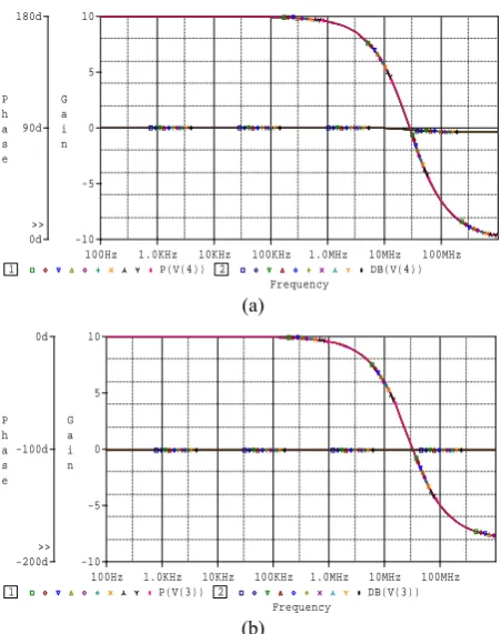
14.4µm/0.18µm. The proposed circuit was designed with C = 5 pF and gate control voltages (VG) as 0.62 V,
0.65 V and 0.71 V. The simulated gain and phase responses are shown in Fig. 3 which depicts the variation in pole frequency at different gate voltages.
Table 2 Aspect ratios of MOS transistors used for simulation.
Transistors W(µm)/L(µm)
M1-M2, M4-M5,M17-M26 1.44/0.18
M3, M6-M10 2.88/0.18
M11-M16 11.51/0.18
M27-M30 0.29/0.18
M31-M32 5.22/0.18
M33 16.19/0.18
M34 3.6/0.18
Frequency
100Hz 1.0KHz 10KHz 100KHz 1.0MHz 10MHz 100MHz 1 P(V(4)) 2 DB(V(4))
0d 90d 180d
P h a s e
>> -10
-5 0 5 10
G a i n
(a)
Frequency
100Hz 1.0KHz 10KHz 100KHz 1.0MHz 10MHz 100MHz 1 P(V(3)) 2 DB(V(3))
-200d -100d 0d
P h a s e
>> -10
-5 0 5 10
G a i n
(b)
Fig. 3 Simulated gain and phase responses of VC-APF (a)
Inverting (Vout1) (b) Non-Inverting (Vout2).
It has been observed from Fig. 3 that the pole frequencies at Vout1 are found to be 10.34 MHz, 15.02
MHz and 27.13 MHz and at Vout2 are found to be 10.23
MHz, 14.82 MHz and 27 MHz. Next to show the voltage swing capability and phase errors, the transient analysis is executed on the proposed circuit at 27 MHz. The simulated input and output waveforms are shown in Fig. 4. It is shown from the results that output waveforms are +900 and -900 phase shifted with the
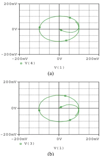
input waveform as expected. Fig. 5 shows the Fourier spectrum of the output waveforms at 27 MHz. In addition, the X–Y pattern (Lissajous pattern) for the two outputs with +900 and -900 phase shifts is also
illustrated in Fig. 6.
Time
0s 20ns 40ns 60ns 80ns 100ns V(1) V(4)
-200mV 0V 200mV
V o l t a g e
(a)
Time
0s 20ns 40ns 60ns 80ns 100ns V(1) V(3)
-200mV 0V 200mV
V o l t a g e
(b)
Fig. 4 Input/output waveforms for first-order VC-APF at 27
MHz (a) Inverting (Vout1) (b) Non-Inverting (Vout2).
Frequency
0Hz 50MHz 100MHz 150MHz 200MHz 250MHz V(1) V(4)
100uV 10mV 150mV
V o l t a g e
(a)
Frequency
0Hz 50MHz 100MHz 150MHz 200MHz 250MHz V(1) V(3)
100uV 10mV 150mV
V o l t a g e
(b)
Fig. 5 Fourier spectrum of input-output waveforms at 27 MHz
(a) Inverting (Vout1) (b) Non-Inverting (Vout2).
V(1)
-200mV 0V 200mV V(4)
-200mV 0V 200mV
(a)
V(1)
-200mV 0V 200mV V(3)
-200mV 0V 200mV
(b)
Fig. 6 X-Y pattern (a) showing +900 phase shift for Vout1 and
-900 phase shift for Vout2 against input voltage at 27MHz.
The input and output noise spectral densities for both responses with respect to frequency are shown in Fig. 7. The equivalent input/output noises are found to be 48.78/47.56 nV/√Hz for Vout1 and 48.97/48.61
nV/√Hz for Vout2, respectively.
Frequency
100KHz 1.0MHz 10MHz 100MHz V(INOISE) V(ONOISE)
44nV 48nV 52nV
(a)
Frequency
100KHz 1.0MHz 10MHz 100MHz V(INOISE) V(ONOISE)
44nV 48nV 52nV
(b)
Fig. 7 Input and output noise variations against frequency for (a) Inverting (Vout1) (b) Non-Inverting (Vout2).
Frequency
100Hz 1.0KHz 10KHz 100KHz 1.0MHz 10MHz 100MHz 1 P(V(4)) 2 DB(V(4))
0d 90d 180d
P h a s e
-10 -5 0 5 10
G a i n
>>
(a)
Frequency
100Hz 1.0KHz 10KHz 100KHz 1.0MHz 10MHz 100MHz 1 P(V(3)) 2 DB(V(3))
-200d -100d 0d
P h a s e
-10 -5 0 5 10
G a i n
>>
(b)
Fig. 8 Frequency responses at different operating temperatures (a) Inverting (Vout1) (b) Non-Inverting (Vout2).
Next, study on the proposed first-order VC-APF is carried out on its temperature performance, the simulated frequency responses at operating temperature range i.e. -40o C to 120o C are shown in Figs. 8(a) and
8(b) for Vout1, and Vout2. Figs. 8(a) and 8(b) shows that
the phase shift is found to vary with frequency while the magnitudes remain almost invariable.
In addition, the Monte Carlo analysis of the proposed circuit of Fig. 2 is done for multiple runs while parameters (the threshold voltage, VT0 and the
process transconductance parameter, K'n) are varied. The Monte Carlo simulation can be done for a Uniform or Gaussian probability distribution. VT0 and K'n are
endorsed to follow a Gaussian deviation of 15% for nominal 10 runs, each varying independently. The gain and phase responses of proposed VC-APF with Monte Carlo analysis with the variations in VT0 are shown in
Fig. 9. Also, Fig. 10 shows the variation in the gain and phase responses with the deviation in K'n. As depicted from the outcomes of Monte-Carlo analysis, the proposed VC-APF has good sensitivity performances.
5 nth Order Voltage Controlled All-Pass Filter
All-pass filters have a unit magnitude response over all the frequencies with the phase change. Therefore, they can be used to realize an nth order all-pass filter
which can be used as an analog group delay equalizers for the video and communication applications [34]-[35].
Frequency
100Hz 1.0KHz 10KHz 100KHz 1.0MHz 10MHz 100MHz 1 DB(V(4)) 2 P(V(4))
-10 -5 0 5 10
G a i n
>> 0d 90d 180d
P h a s e
(a)
Frequency
100Hz 1.0KHz 10KHz 100KHz 1.0MHz 10MHz 100MHz 1 DB(V(3)) 2 P(V(3))
-10 -5 0 5 10
G a i n
>> -200d -100d 0d
P h a s e
(b)
Fig. 9 Monte Carlo analysis with the variations in VT0 showing
all-pass response (a) Inverting (Vout1) (b) Non-Inverting (Vout2).
Frequency
100Hz 1.0KHz 10KHz 100KHz 1.0MHz 10MHz 100MHz 1 P(V(4)) 2 DB(V(4))
0d 90d 180d
P h a s e
>> -10
-5 0 5 10
G a i n
(a)
Frequency
100Hz 1.0KHz 10KHz 100KHz 1.0MHz 10MHz 100MHz 1 P(V(3)) 2 DB(V(3))
-200d -100d 0d
P h a s e
>> -10
-5 0 5 10
G a i n
(b)
Fig. 10 Monte Carlo analysis with the variations in K'n
showing all-pass response (a) Inverting (Vout1) (b) Non-Inverting (Vout2).
The nth order all-pass filter is realized by connecting
the n-number of first-order all-pass filters in cascade [36]. By exploiting the feature of the first-order VC-APF i.e. the availability of one output Vout2 at low
output impedance terminal, an nth order filter is further
realized as shown in Fig. 11. The proposed nth order
VC-APF employs n-stages of DV-DXCCII, n-NMOS transistor biased in the triode region and n-grounded capacitors.
Analysis of the proposed circuit of Fig. 11 yields the following two transfer functions.
( )
( )
1 1 1 2 2
1 1 2 2
1 1
1
1 1
1 1
n
out n MOS MOS
in MOS MOS
n MOSn
n MOSn
V sC R sC R
V sC R sC R
sC R sC R
⎛ − ⎞ ⎛ − ⎞
= − ⎜ ⎟ ⎜× ⎟×
+ +
⎝ ⎠ ⎝ ⎠
⎛ − ⎞
×⎜ + ⎟
⎝ ⎠
""
(15)
2( ) 1 1 2 2
1 1 2 2
1 1
1 1
1 1
out n MOS MOS
in MOS MOS
n MOSn
n MOSn
V sC R sC R
V sC R sC R
sC R sC R
⎛ − ⎞ ⎛ − ⎞
=⎜ ⎟ ⎜× ⎟×
+ +
⎝ ⎠ ⎝ ⎠
⎛ − ⎞
×⎜ + ⎟
⎝ ⎠
""
(16)
The angular resonance frequency (ωo(n)) can be
expressed as
( )
1
1 2 1 2
1
( ... ) ( ... )
n
o n
n MOS MOS MOSn
C C C R R R
ω = ⎜⎛ × ⎞⎟
⎝ ⎠ (17)
To illustrate the utility of the proposed nth order
VC-APF, a third-order all-pass filter circuit is implemented with n = 3 (three DV-DXCCII, three NMOS transistors
and three grounded capacitors). Putting n = 3 in Eq. (15) and Eq. (16), the two transfer functions are modified as
( )
( )
31 3 1 1 2 2
1 1 2 2
3 3
3 3
1 1
1
1 1
1 1
out MOS MOS
in MOS MOS
MOS
MOS
V sC R sC R
V sC R sC R
sC R sC R
⎛ − ⎞ ⎛ − ⎞
= − ⎜ ⎟ ⎜× ⎟
+ +
⎝ ⎠ ⎝ ⎠
⎛ − ⎞
×⎜ + ⎟
⎝ ⎠
(18)
2(3) 1 1 2 2
1 1 2 2
3 3
3 3
1 1
1 1
1 1
out MOS MOS
in MOS MOS
MOS
MOS
V sC R sC R
V sC R sC R
sC R sC R
⎛ − ⎞ ⎛ − ⎞
=⎜ ⎟ ⎜× ⎟
+ +
⎝ ⎠ ⎝ ⎠
⎛ − ⎞
×⎜ + ⎟
⎝ ⎠
(19)
Equation (18) and (19) are the third-order inverting and non-inverting all-pass transfer functions. The angular resonance frequency ωo(3) by putting n = 3 in eq.
(17) is given by
( )
1 3 3
1 2 3 1 2 3
1
( ) ( )
o
MOS MOS MOS
C C C R R R
ω = ⎜⎛ ⎞⎟
×
⎝ ⎠ (20)
The third-order all-pass circuit is designed by taking C1 = C2 = C3 = 5 pF and gate control voltage VG1 = VG2
= VG3 = 0.62 V, 0.71 V and 0.8 V. The simulated gain
and phase responses are shown in Fig. 12 which shows the variation in angular resonant frequency at different gate voltages. It can be seen that the pole frequency at
Vout1(3) are found to be 10.32 MHz, 14.97 MHz and
27.02 MHz and at Vout2(3) are found to be 10.13 MHz,
14.62 MHz and 26.92 MHz.
Fig. 11 nth-order voltage controlled all-pass filter.
Frequency
100Hz 1.0KHz 10KHz 100KHz 1.0MHz 10MHz 100MHz 1.0GHz 1 P(V(24)) 2 DB(V(24))
-387d -193d -0d 180d
P h a s e
-10 -5 0 5 10
G a i n
>>
Frequency
100Hz 1.0KHz 10KHz 100KHz 1.0MHz 10MHz 100MHz 1.0GHz 1 P(V(23)) 2 DB(V(23))
-600d -400d -200d 0d
P h a s e
-10 -5 0 5 10
G a i n
>>
(a) (b)
Fig. 12 Simulated gain and phase responses of third order VC-APF (a) Inverting (Vout1(3)) (b) Non-Inverting (Vout2(3)).
6 Conclusion
A new voltage controlled first order all-pass filter, employing single DV-DXCCII as active component, one NMOS transistor biased in triode region and one grounded capacitor as passive component is proposed. The given circuit enjoys the features of resistorless structure, use of grounded capacitor, use of single active element, minimum components requirement for first order all-pass filter, inverting and non-inverting all-pass responses simultaneously and controlling of filter pole frequency through external voltage. Non-ideal analysis is also discussed. As an application, an nth order all-pass
filter employing the proposed filter connected in cascade is also presented. The circuits are found to show good frequency performance, which makes them superior to existing works. Simulations results are given to confirm the presented theory.
References
[1] S. Minaei and O. Çiçekoglu, “A Resistorless realization of the first-order all-pass filter”, International Journal of Electronics, Vol. 93, No. 3, pp. 177-183, 2006.
[2] S. Maheshwari, “High input impedance VM-APSs with grounded passive elements”, IET Circuits, Devices and Systems, Vol. 1, No. 1, pp. 72-78, 2007.
[3] S. Maheshwari, “A canonical voltage-controlled VM-APS with grounded capacitor”, Circuits, Systems and Signal Processing, Vol. 27, No. 1, pp. 123-132, 2008.
[4] S. Maheshwari, “High input impedance voltage-mode first-order all-pass sections”, International Journal of Circuit Theory and Applications, Vol. 36, No. 4, pp. 511-522, 2008.
[5] A. U. Keskin, K. Pal and E. Hancioglu, “Resistorless first order all-pass filter with electronic tuning”, AEU-International Journal of Electronics and Communications, Vol. 62, No. 4, pp. 304-306, 2008.
[6] N. Herencsar, J. Koton, and K. Vrba, “A new electronically tunable voltage-mode active-C phase shifter using UVC and OTA”, IEICE Electronics Express, Vol. 6, No. 17, pp. 1212-1218, 2009.
[7] S. Minaei and E. Yuce, “Novel voltage-mode all-pass filter based on using DVCCs”, Circuits, Systems, and Signal Processing, Vol. 29, No. 3, pp. 391-402, 2010.
[8] T. Tsukutani, H. Tsunetsugu, Y. Sumi, and N. Yabuki, “Electronically tunable first-order all-pass circuit employing DVCC and OTA”, International Journal of Electronics, Vol. 97, No. 3, pp. 285-293, 2010.
[9] S. Minaei, and E. Yuce, “High input impedance NMOS based phase shifter with minimum number of passive elements”, Circuits, Systems,
and Signal Processing, Vol. 31, No. 1, pp. 51-60, 2012.
[10] S. Maheshwari, J. Mohan, and D. S. Chauhan, “Novel voltage-mode cascadable all-pass sections employing grounded passive components”, Journal of Circuits, Systems, and Computers, Vol. 22, Article ID 1250065, 2013.
[11] I. A. Khan and M. T. Ahmed, “Electronically tunable first-order OTA-capacitor filter sections”, International Journal of Electronics, Vol. 61, No. 2, pp. 233-237, 1986.
[12] A. M. Soliman, “Generation of current conveyor-based all-pass filters from op amp-conveyor-based circuits”, IEEE Transactions on Circuits and Systems II: Analog and Digital Signal Processing, Vol. 44, No. 4, pp. 324-330, 1997.
[13] A. Toker, S. Özcan, H. Kuntman and O. Çiçekoglu, “Supplementary all-pass sections with reduced number of passive elements using a single current conveyor”, International Journal of Electronics, Vol. 88, No. 9, pp. 969-976, 2001. [14] S. Maheshwari and I. A. Khan, “Novel first order
all-pass sections using a single CCIII”, International Journal of Electronics, Vol. 88, No. 7, pp. 773-778, 2001.
[15] M. A. Ibrahim, H. Kuntman, and O. Çiçekoglu, “First-order all-pass filter canonical in the number of resistors and capacitors employing a single DDCC”, Circuits, Systems, and Signal Processing, Vol. 22, No. 5, pp. 525-536, 2003. [16] H. P. Chen and K. H. Wu, “Grounded-capacitor
first-order filter using minimum components”, IEICE Transactions of Fundamentals, Vol. E89- A, pp. 3730-3731, 2006.
[17] M. A. Ibrahim, H. Kuntman, S. Ozcan, O. Suvak, and O. Çiçekoglu, “New first-order inverting-type second-generation current conveyor-based all-pass sections including canonical forms”, Electrical Engineering, Vol. 86, No. 5, pp. 299-301, 2004.
[18] S. Maheshwari, “Voltage-mode all-pass filters including minimum component count circuits”, Active and Passive Electronic Components, Vol. 2007, Article ID 79159, 5 pages, 2007.
[19] S. Minaei and E. Yuce, “Unity/variable-gain voltage-mode/current-mode first-order all-pass filters using single dual-X second-generation current conveyor”, IETE Journal of Research, Vol. 56, No. 6, pp. 305-312, 2010.
[20] S. Maheshwari, J. Mohan and D. S. Chauhan, “Voltage-mode cascadable all-pass sections with two grounded passive components and one active element”, IET Circuits, Devices and Systems, Vol. 4, No. 2, pp. 113-122, 2010.
[21] D. Biolek and V. Biolkova, “First-order voltage-mode all-pass filter employing one active element and one grounded capacitor”, Analog Integrated
Circuits and Signal Processing, Vol. 65, No. 1, pp. 123-129, 2010.
[22] N. Herencsar, J. Koton, J. Jerabek, K. Vrba and O. Çiçekoglu, “Voltage-mode all-pass filters using universal voltage conveyor and MOSFET-based electronic Resistors”, Radioengineering, Vol. 20, No. 1, pp. 10-18, 2011.
[23] S. Maheshwari and B. Chaturvedi, “High-input low-output impedance all-pass filters using one active element”, IET Circuits, Devices and Systems, Vol. 6, No. 2, pp. 103-110, 2012.
[24] N. Herencsar, S. Minaei, J. Koton, E. Yuce and K. Vrba, “New resistorless and electronically tunable realization of dual-output VM all-pass filter using VDIBA”, Analog Integrated Circuits and Signal Processing, Vol. 74, No. 1, pp. 141-154, 2013.
[25] F. Yucel and E. Yuce, “CCII based more tunable voltage-mode all-pass filters and their quadrature oscillator applications”, International Journal of Electronics and Communication (AEÜ), Vol. 68, No. 1, pp. 1-9, 2014.
[26] S. Maheshwari and D. Agrawal, “High performance voltage-mode tunable all-pass section”, Journal of Circuits, Systems, and Computers, Vol. 24, No. 6, (12 pages), 2015. [27] P. Beg, “Tunable first-order resistorless all-pass
filter with low output impedance”, The Scientific World Journal, article ID 219453, 2014 (6 pages). [28] W. Tangsrirat, J. Budboonchu and T. Pukkalanun, “Resistorless voltage-mode first-order allpass section using single current-controlled conveyor transconductance amplifier”, Indian Journal of Pure & Applied Physics, Vol. 53, No. 5, pp. 335-340, 2015.
[29] J. W. Horng, C. M. Wu and N. Herencsar, “Fully differential first-order allpass filters using a DDCC”, Indian Journal of Engineering and Materials Sciences, Vol. 21, No. 4, pp. 345-350, 2014.
[30] J. Mohan and S. Maheshwari, “Additional high-Input low-output impedance voltage-mode all pass section”, Journal of Circuits, Systems, and Computers, Vol. 23, No. 6, 2014 (14 pages). [31] H. O. Elwan and A. M. Soliman, “Novel CMOS
differential voltage current conveyor and its applications”, IEE Proceeding Circuits Devices and Systems, Vol. 144, No. 3, pp. 195-200, 1997. [32] S. Minaei, and E. Yuce, “A new full-wave
rectifier circuit employing single dual-X current conveyor”, International Journal of Electronics, Vol. 95, No. 8, pp. 777-784, 2008.
[33] M. Bhusan and R. W. Newcomb, “Grounding of Capacitors in Integrated Circuits”, Electronics Letters, Vol. 3, No. 4, pp. 148-149, 1967. [34] E. G. Cristal, “Theory and design of transmission
line all-pass equalizers”, IEEE Transactions on Microwave Theory and Techniques, Vol. 17, No. 1, pp. 28-38, 1969.
[35] S. Abielmona, S. Gupta and C. Caloz, “Compressive receiver using a CRLH based dispersive delay line for analog signal processing”, IEEE Transactions on Microwave Theory and Techniques, Vol. 57, No. 11, pp. 2617-2626, 2009.
[36] D. Biolek, J. Cajka, K. Vrba and V. Zeman, “nth
-order all-pass filters using current conveyors”, Journal of Electrical Engineering, Vol. 53, No. 1-2, pp. 50–53, 2002.
Bhartendu Chaturvedi received B. Tech. degree in Electronics & Communication Engineering in 2005 and M.Sc. Tech. degree in Electronics Engineering, with specialization in Electronic Circuits and System Design in 2008. He has completed his Ph.D. in Electronics Engineering from Department of Electronics Engineering of Aligarh Muslim University, Aligarh, India in 2014. He is currently working as Assistant Professor in the Department of Electronics and Communication Engineering of Jaypee Institute of Information Technology, Noida, India. His research interests include Analog Signal Processing, Circuits & Systems. He has published around 30 research papers in reputed international journals & conferences and also authored 1 book chapter.
Jitendra Mohan obtained his B. Tech.
degree from S. R. T. M. University, Nanded in 2001. He got his M.Tech degree from Aligarh Muslim University in 2005 and Ph.D. degree from Uttarakhand Technical University in 2011. He is currently working as an Assistant Professor in the Department of Electronics and Communication Engineering at Jaypee Institute of Information Technology, Noida (India). His main areas of interest are current-mode circuits and analog signal processing applications. He has guided 01 Master’s Dissertation and 13 projects. He has more than 45 International Journal and conference papers.