Volume 8, Number 4, pp. 373–385.http://www.scpe.org 2007 SWPS
PERFORMANCE OF A LU DECOMPOSITION ON A MULTI-FPGA SYSTEM COMPARED TO A LOW POWER COMMODITY MICROPROCESSOR SYSTEM∗
T. HAUSER†, A. DASU‡, A. SUDARSANAM‡ , AND S. YOUNG‡
Abstract. Lower/Upper triangular (LU) factorization plays an important role in scientific and high performance computing. This paper presents an implementation of the LU decomposition algorithm for double precision complex numbers on a star topology based multi-FPGA platform. The out of core implementation moves data through multiple levels of a hierarchical memory system (hard disk, DDR SDRAMs and FPGA block RAMS) using completely pipelined data paths in all steps of the algorithm. Detailed performance numbers for all phases of the algorithm are presented and compared to a highly optimized implementation for a low power microprocessor based system. We also compare the performance/Watt for the FPGA and the microprocessor system. Finally, recommendations will be given on how improvements of the FPGA design would increase the performance of the double precision complex LU factorization on the FPGA based system.
Key words. LU factorization, multi-FPGA system, benchmarking
1. Introduction. High-performance reconfigurable computers (HPRC) [20, 5] based on conventional pro-cessors and field-programmable gate arrays (FPGAs) [31] promise better performance, especially when taking the power consumption into account. Recently, HPRCs have shown orders of magnitude improvements in performance, e.g. power and speed, over conventional high-performance computers (HPCs) in some compute intensive integer applications but showing similar success on floating point based problems has been limited [32]. Scientific computing applications demand double-precision arithmetic because of numerical stability and large dynamic range requirements. Solving linear systems and linear algebra plays an important role in scientific and high performance computing. The LAPACK library [1, 2, 10, 12, 13, 36, 3, 7] is a high quality library of linear equation solvers and considerable work has been done to achieve very good performance on different high performance computing platforms. The introduction of hierarchical memory systems, which feature multiple levels of cache storage with different sizes and access speeds, has tended to degrade the performance of these linear algebra routines compared to the peak performance. Obtaining good performance with such systems required the formulation of those algorithms in terms of operations on blocks, so that cache misses could be minimized [16].
The goal of this paper is to benchmark and compare the performance of a block based algorithm on a HPRC platform to a highly optimized implementation on a commodity microprocessor. and provide suggestions for the improvement of the FPGA platform to better support floating point linear algebra algorithms. Our work is based on the algorithms described in [10] which is adapted to a specific class of HPRCs. Hardware-based matrix operator implementation has been addressed by several researchers. Ahmed El-Amawy [15] proposes a systolic array architecture consisting of (2N2−N) processing elements which computes the inverse in O(N) time, whereN is the order of the matrix. However, there are no results to show that the large increase in area (for large values ofN) is compensated by the speed of this implementation.
Power efficiency is a critical issue in current high performance computing facilities and a critical issue for developing cost effective small-footprint clusters [22] as it directly influences the cooling requirements of each cluster node and of the overall cluster rack and server room layout. A 48 core, low power cluster [29], designed to run on 20 Amp electric circuit, is an example of per-node low power requirements. Each of our quad-core processor nodes consumes approximately 78 Watts during normal operation under our group’s cluster workloads. We describe the design and implementation of the LU factorization algorithm for a double precision complex matrix on a HPRC system and compare it to a highly tuned implementation for a commodity microprocessor. The matrices considered for the factorization are so large that the factorization has to be performed out of core on the FPGA system. In addition to comparing the wall clock times, power efficiency of the FPGA versus the microprocessor using the millions of floating point operations per Watt (MFlops/Watt) metric is provided.
The paper is structured as follows. Section 2 describes the general multi-FPGA system architecture the algorithm is designed for and the details of the Starbridge HC-62 system. Section 3 presents an overview of the
∗This work was support in part by Lockheed Martin Corp.
†Center for High Performance Computing, Utah State University, 4175 Old Main Hill, Logan, UT, 84322-4175
‡Department of Electrical and Computer Engineering, Logan, UT, 4120 Old Main Hill, Logan, UT, 84322-4120
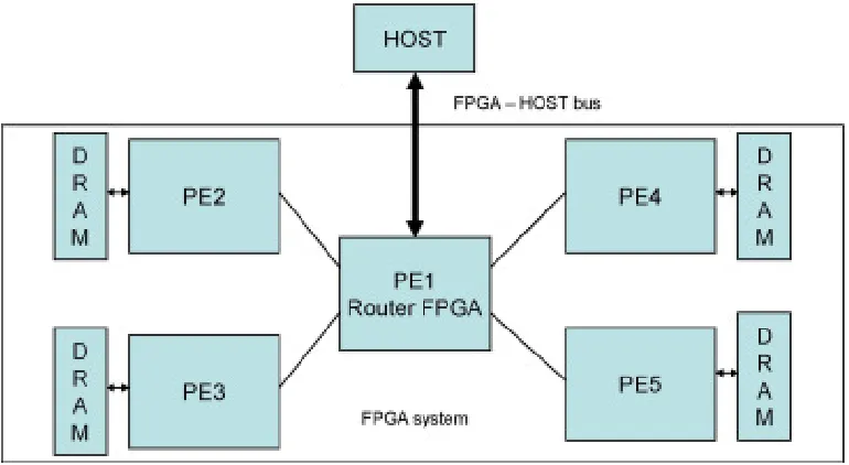
Fig. 2.1.Star topology based multi-FPGA system with four FPGAs
algorithm used and how it is mapped on the HPRC architecture. In Sections 4 and 5 we discuss the benchmark results and compare it to the commodity microprocessor implementation. Section 6 presents an overview over related work for floating point computation on HPRC architectures and Section 7 provides the lessons learned from this implementation.
2. Multi-FPGA system architecture.
2.1. Star networked FPGAs with external storage. The hardware system topology we have con-sidered for analysis and mapping of the LU factorization algorithm is the Star Network Topology. We assume that in this topology, multiple FPGA devices can communicate to a central host microprocessor through a concentrator/router FPGA. In addition, each FPGA is assumed to have its own local external storage such as DRAM chips. We refer to this structure henceforth as “Star Networked FPGAs with Local Storage” or SNFLS topology. Figure 2.1 shows a SNFLS systems with four compute FPGAs (PE2-PE5) with locally attached DRAM, one router FPGA and the host system. Several variations in the topology, such as the manner how physical memory devices are distributed across FPGAs, how the accelerator FPGA board is connected to a host system, etc. can have impacts on the performance of a system.
2.2. Starbridge HC-62 system. The system used for the implementation and benchmarks contains a HC-64 board from Starbridge systems, consisting of eight programmable FPGAs, attached to a host PC with an Intel x86 processor. There are two FPGA chips that are used for interface functions. The first is an Xpoint switch chip, and the second is a primary function chip, PE1. The Xpoint FPGA provides a link between the other FPGAs and the PCI bus. It provides a 256-bit fully populated synchronous cross-point router with each of the four FPGA elements PE2 through PE5 at 82.4 Gigabits/second. The four FPGAs are connected through a 128-bit data bus to the Xpoint and PE1 chips, and each contain two 128-bit serial multiplier objects. A group of four FPGA connected together with 50-bit parallel lines is called a quad group. Each quad group is internally connected with a 50-bit exclusive chip to chip bus at 96.6 gigabits per second. The memory chips attached to each PE are arranged in four banks around the chip. The main memory is made up of 8-72 Gigabytes SDRAM modules, with a bandwidth of 95 Gigabytes with 36 independent 64 bit ports. Each PE is a Xilinx Virtex-II chip. It consists of 33,792 slices, with each slice consisting of 2 Flip-Flops (FFs) and 2 Look-Up Tables (LUTs). The chip also contains 144 18x18 ASIC multipliers and 144 Block RAMs (BRAMS) and each RAM contains 18K bits of memory.
3. Matrix Factorization implementation for a multi-FPGA system.
permutation matrix is not necessary, since all matrices from the problem addressed are diagonally dominant and the condition number of our matrices is ofO(1). Lis a unit lower triangular matrix with 1’s on the main diagonal,U is an upper triangular matrix. Our algorithm is applied recursively by partitioning the matrixA(k),
which is an×nsubmatrix of sizen=N−(k−1)·nbat thek-th step into four blocks, wherenb is our blocking size.
A(k)=L(k)U(k)= A
(k) 11 A
(k) 12 A(21k) A(22k)
!
(3.1)
= L
(k) 11 0 L(21k) L(22k)
!
U11(k) U12(k)
0 U22(k)
!
(3.2)
= L
(k) 11U
(k)
11 L
(k) 11U
(k) 12 L(21k)U
(k) 11 L
(k) 21U
(k) 12 +L
(k) 22U
(k) 22
!
where the dimensions of the blockA(11k)arenb×nb, ofA(21k)arenb×(n−nb),ofA21(k)are (n−nb)×nb, and
ofA(22k)are (n−nb)×(n−nb). The block partitioned algorithm at thek-th recursion step is performed in four steps:
1. A(11k) is factored intoU11(k)andL(11k). 2. A(21k) is factored intoL(21k).
3. U12(k)is computed by solving the triangular system
L(11k)U (k) 12 =A
(k)
12 (3.3)
in our implementationU12(k)is computed using the inverse ofL(11k)
U12(k)←L(k)
11
−1
A(12k) (3.4)
The use of the inverse ofL(11k)is more efficient according to Ditkowski [11], since the condition number of our matrices is always ofO(1).
4. Update the remaining blockAe(22k), which then becomes the matrixAk for the next iterationk+ 1.
e
A(22k)←A(k)
22 −L (k) 21U
(k) 12 =L
(k) 22U
(k)
22 (3.5)
The LU factorization is completed when the matrixA(k) becomes so small that only step 1 is left to
compute.
3.2. Mapping of the LU algorithm onto a multi-FPGA system. The SNFLS architecture as shown in Figure 2.1 is particularly suited for the block-based dense matrix LU factorization, as this algorithm has no need for inter-block communication in any of the sub-steps. Input data can be loaded into each of the DRAMs and processed and written back to the host. By analyzing the algorithm, it can be observed that there is data re-use at both the intra-block as well at the inter-block level. Therefore, a set of blocks can be initially loaded onto the DRAMs from PC memory and one block can be loaded onto an FPGA’s BRAM for execution. We assume that most of the data resides on the hard disk of the host microprocessor, and these storage devices are slow, since they need to communicate with FPGA DRAMs through the PCI-X bus. The data is first transferred from hard disk to host processor memory. Then it is routed through the host-FPGA bus and saved on each FPGA’s DRAM.
The top level control flow can be handled by the host processor which will split the matrix into multiple parts for each step. On-chip memory of the host processor can be used as a buffer to handle the difference in the speed of data transfer between Host’s-Hard Disk and an FPGA. Data transfer between off-chip DRAM and the FPGA is modeled as a sequence of I/O operations. During a single I/O operation, a block of data can be transferred from off-chip DRAM to the FPGA. This block is of sizenb×nb, wherenbis the block size in the LU
too small, nor too large. A too small value of nb is wasting opportunities for parallelism whereas a too large
value will exceed the capacity of the DRAM.
When data is transferred from host memory to DRAM, one of the factors that can limit the amount of data transferred per I/O operation is the DRAM size. Information about the latency of transferring data from host memory to DRAM should be used while scheduling the various operations.
The proposed design outlines the order in which the various blocks of data are transferred from/to the host memory to/from the FPGA board. The number of blocks transferred will depend on the DRAM size associated with each FPGA. The following sequence of control steps determines the order of their access.
For the case of a single-FPGA accelerated system, a basic block of sizenb×nb forms the input and the
module corresponding to the algorithm in which a single block is processed needs to be realized in FPGA hardware. In the proposed approach, data path units found inside the inner-most loop are identified and these units are replicated as many times as possible on a given FPGA device. The number of parallel instances is limited by resource availability of a single FPGA, as the proposed design limits the processing of a single block of data to be performed within a single FPGA. This constraint is added so that the data transfer logic can be localized to a single FPGA permitting easy scalability if more FPGAs are added to the system, but topology is retained.
From preliminary investigation, it was concluded that a single moderate size FPGA (such as a Xilinx Virtex 2-6000) can provide some amount of data path parallelism if the data types are single precision and real. But even these expensive devices do not have sufficient resources to support data path parallelism within a chip if the data types are complex and double precision floating point. In such cases since intra-block parallelism is limited, there is a need to extract inter-block parallelism by using multiple FPGAs to execute several blocks in parallel. For effective use of all three levels of memory in the system, initial data is assumed to be stored in the hard disk that is connected to the host processor. Each FPGA contains block RAMs (BRAMS) that form the first level of the memory hierarchy and provide seamless bandwidth to computation modules on the device. Resource utilization of BRAMs depends on multiple factors that include block size, amount of parallelism required, data type etc and is limited by the amount of on-chip memory available. Off-chip DRAMs form the second level of memory hierarchy and bandwidth between compute engine and DRAM is limited by the interconnection between FPGA and DRAM. Hard disks (connected via the host computer) form the third level in memory hierarchy.
Since the matrices generally are so big that computing the LU decomposition on a single PE is prohibitively expensive, the different steps are distributed onto several FPGAs so don’t processing can take part in parallel. Steps 1 is processed on the host PC since it is only computed once and then the result is distributed to the different FPGAs. Figure 3.1a shows how steps 2 and 3 can be mapped to multiple FPGAs. Half of the FPGAs are assigned to process the submatrix A(21k). This matrix is than partitioned in as many parts as FPGAs are
available for processing. The same approach is taken to processA(12k). Figure 3.1b shows how the matrixA(22k)is distributed to multiple PEs. Together with the part ofA(22k) that is assigned to a PE, the corresponding parts ofA(21k) andA12(k) necessary to compute the resultsAe(22k) are also copied to the PE.
4. Benchmarking results of a double-precision complex LU decomposition. We implemented the algorithm described in Section 3 using Viva 3.0. Viva, developed by Starbridge systems, is a graphic-based hard-ware design tool to generate and synthesize the hardhard-ware designs for the LU decomposition algorithm. Xilinx mapping and place-and-route tools were used to generate the bit streams for the designs that then were loaded onto the target hardware platform. Our implementation was benchmarked on a Starbridge Hypercomputer board HC-36 (see Section 2.2). Although the IP cores for individual arithmetic units can be clocked at 100MHz or higher, the vendor caps the board to run only at 66MHz. Matrix sizes varied from 1000x1000, 2000x2000, 4000x4000 and 8000x8000. Each element in once of the matrices is a 64-bit double precision (52- mantissa; 11-exponent; 1-sign) complex number. In the discussion of the performance result the following four phases in the computation are differentiated:
1. Reconfiguration: The FPGA needs to be reconfigured for each of the four steps of the LU factorization. 2. FPGA processing: This time includes the transfer from DRAM to BRAM and all computational
pro-cessing on the FPGA and the transfer back to DRAM.
3. PC to DRAM: This time describes the time takes to transfer data from the host PC to the DRAM of the FPGA accelerator.
(a) Step 2 and Step 3 mapping to multiple FPGAs (b) Step 4 mapping to multiple FPGAs
Fig. 3.1.Mapping of different steps of the algorithm to multiple FPGAs
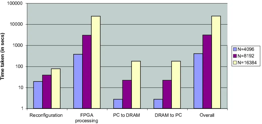
Fig. 4.1. Wall clock times for the different phases of the LU implementation for increasing problem sizes N on one FPGA
shown on a log scale (nb= 1)
4.1. Performance depending on problem size. In Figure 4.1, run-times for several problem sizes are compared for each of the different phases of the algorithm. The run times are displayed on a logarithmic scale because otherwise it would be difficult to recognize the small contributions of the reconfiguration, PC to DRAM transfer and DRAM to PC phases to the overall time of the algorithm.
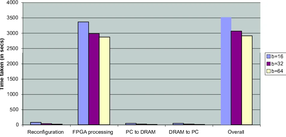
4.2. Performance Depending on Block Size. The block size nb is an important parameter of the
block partitioned LU factorization algorithm. This parameter determines how big the pieces are the FPGA can process on. In Figure 4.2, the influence of different block sizesnb on the performance is shown.
Fig. 4.2.Wall clock times of different phases of the LU implementation for increasing block sizenbon one FPGA (N= 8192)
The block sizenbcannot be increased above 64 because of the limitation on the number of block RAMs on
the used FPGA. Increasing the block size increases the performance of the algorithm not only in the compute engine but it also reduces the number of blocks transferred and the number of reconfigurations. These are overhead operations which do not contribute to the overall progress of the computation but are necessary for the implementation of the algorithm.
4.3. Performance depending on number of FPGAs. In Figure 4.3 the wall clock times for the different phases of the LU algorithm are presented, when the number of FPGAs is increased.
Similar to figure 4.1, the dominating time is the processing time in the FPGA. The memory transfer time stays constant because of the the star topology of the hardware. All data has to go through the PCI bus to the DRAM of the individual FPGA. Therefor no speedup can be achieved for the memory transfer. The reconfiguration time actually increases when the number of FPGAs is increased.
The speedupS, defined as
S= Ts
Tn p
, (4.1)
is given in table 4.1. Tsis the time on a system with one FPGA andTpnis the time of the parallel algorithm
onn FPGAs. The result show that the overall speedup does not scale linearly with increasing the number of FPGAs. While performance on each FPGA is highly deterministic, one can and correctly expect a linear scaling in speedup if only FPGA processing times are inspected. But because of the overhead of the data transfer and reconfiguration the speedup is reduced significantly.
Table 4.1
Speedup computed from increasing the number of FPGAs for block size 64, matrix size 8192
1 FPGA 2 FPGAs 4 FPGAs
Overall time 3870.24 2484.06 1862.41
Fig. 4.3.Wall clock times of the LU decomposition using 1, 2 and 4 FPGAs for processing in log scale
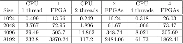
Table 5.1
Comparison of wall clock time between Intel®Xeon®X3210 microprocessor and FPGA implementation with block size = 64
CPU 1 CPU 2 CPU 4
Size 1 thread FPGA 2 threads FPGAs 4 threads FPGAs
1024 0.499 13.56 0.249 16.24 0.318 26.03
2048 3.767 72.95 1.896 61.67 1.066 73.47
4096 29.49 505.7 14.862 348.74 8.021 305.69
8192 232.8 3870.24 117.2 2484.06 61.73 1862.41
5. Performance comparison to a commodity microprocessor.
5.1. Microprocessor based system architecture and LU implementation. For comparison the per-formance and power consumption was measured on a low power commodity CPU cluster which was specifically designed to run on a single 20A 110V circuit [29]. Since the problem sizes considered are relatively small a single compute node of this cluster was used to get the performance numbers for the microprocessor based system. The compute node consists of the following components:
• Quad-Core Intel®Xeon®X3210 processors • 8 Gigabytes RAM
• 4 Gigabit ports • No Hard Drive
The implementation of the LU decomposition on the cluster node uses the Intel®MKL library version 9.1 [23], specifically the LAPACK routine “zgetrf”. This library is highly optimized for Intel®processors and provides highly scalable implementations for multiple threads.
5.2. Wall clock time comparison between FPGA and microprocessor based system. The bench-mark results are summarized in Table 5.1.
These results show that the microprocessor has a performance advantage of about 30 times. The perfor-mance of the FPGA implementation could be improved by a factor of two by switching from the floating point objects provided by VIVA to Xilinx Coregen IP cores (see also section 5.3).
Fig. 5.1.LU timing results for Virtex-II 6000 and Virtex-4 LX160 from our performance model
for any FPGA from their respective data-sheets. Hence, our model can be extended to support any multi-FPGA platform. Here we compare the performance model result for a Xilinx Virtex-4 LX160 FPGA with the overall timing results from our benchmark platform using Xilinx Virtex-II 6000 FPGAs. For each target FPGA the number of data paths,P, is set such that the resource utilization of the FPGA is maximum. We foundP = 5 for the Virtex-4 and P = 1 for the Virtex-1 device. In addition we included the effect of switching from the floating point objects provided by the Viva Corelib to the Xilinx IP Coregen library in our performance model results.
Figure 5.1 shows the comparative results for the two target platforms for different values of the problem size,N and a blocking size ofb= 16. It is seen that the Virtex-4 implementation is almost four times faster than the Virtex-II implementation. There is a two-fold increase. One is due to the larger slice count available and the other is use of a better design library.
5.4. Power consumption.
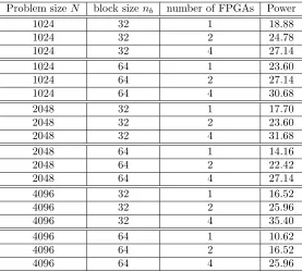
5.4.1. Power consumption of FPGA board. Table 5.2 shows the power consumption of the FPGA board alone. It shows that there is an increase of power consumption with the number of FPGAs used in the computation and the block size.
5.4.2. Power consumption of FPGA system. The overall system, consisting of the host PC and the FPGA board, has a power consumption profile as shown in Table 5.3. An interesting observation is the power consumption for larger problem sizes which seems to go down with the block sizenb. Especially for the largest
test case of 4096×4096 elements the increase in block size shows a reduction in power by ten Watts.
Table 5.2
FPGA board power consumption
Problem sizeN block sizenb number of FPGAs Power
1024 32 1 1.23
1024 32 2 2.70
1024 32 4 6.19
1024 64 1 1.28
1024 64 2 2.85
1024 64 4 6.24
2048 32 1 1.82
2048 32 2 3.04
2048 32 4 6.68
2048 64 1 1.67
2048 64 2 3.29
2048 64 4 6.97
4096 32 1 2.01
4096 32 2 3.73
4096 32 4 7.07
4096 64 1 1.87
4096 64 2 3.63
4096 64 4 7.27
Table 5.3
The Hypercomputer HC System power consumption.
Problem sizeN block sizenb number of FPGAs Power
1024 32 1 18.88
1024 32 2 24.78
1024 32 4 27.14
1024 64 1 23.60
1024 64 2 27.14
1024 64 4 30.68
2048 32 1 17.70
2048 32 2 23.60
2048 32 4 31.68
2048 64 1 14.16
2048 64 2 22.42
2048 64 4 27.14
4096 32 1 16.52
4096 32 2 25.96
4096 32 4 35.40
4096 64 1 10.62
4096 64 2 16.52
4096 64 4 25.96
5.5. Performance per Watt comparison between FPGA and microprocessor based system.
Table 5.4
The Hypercomputer HC System power consumption.
Operating conditions of compute node Power (Watts)
idle 75.5
boot up 131
1 thread benchmark run 113.5
2 thread benchmark run 138.5
4 thread benchmark run 176.5
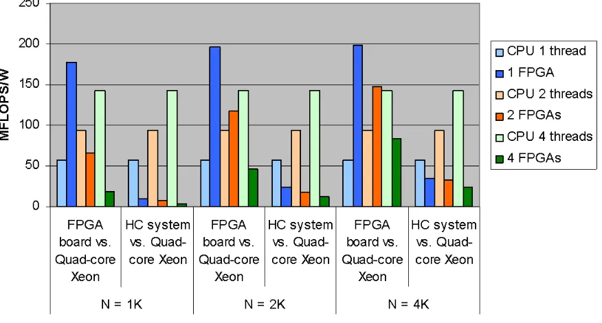
Fig. 5.2. Performance/watt comparison of FPGA board and FPGA system with respect to a low power Quad core Xeon system for various matrix sizes
superior compared to the Quad core system. This can be attributed to the extremely low power consumption of the FPGA devices. These results show that even for a cluster which was specifically designed for low power usage the FPGA system has a clear power advantage.
6. Related and complementary work. Hardware-based matrix operator implementation has been ad-dressed by several researchers. Ahmed-El Amawy [15] proposes a systolic array architecture consisting of (2N2−N) processing elements which computes the inverse inO(N) time, whereN is the order of the matrix. However, there are no results to show that the large increase in area (for large values ofN) is compensated for by the benefits obtained in speed by this implementation.
Lau et. al [25] attempt to find the inverse of sparse, symmetric and positive definite matrices using designs based on Single Instruction Multiple Data (SIMD) and Multiple Instruction Multiple Data (MIMD) architec-tures. This method is limited to a very specific sub-set of matrices and not applicable for a generic matrix and hence has limited practical utility. Edman and Owall [14] also targeted only triangular matrices.
Data et. al [9] propose a single and double precision floating point LU decomposition implementation based on a systolic array architecture described in [8]. The systolic array architecture is a highly parallel realization and requires only a limited communication bandwidth. However, every element in the systolic array needs to have local memory and a control unit in addition to a computation unit, which adds significant overhead.
Wang and Ziavras [34] propose a novel algorithm to compute a LU decomposition for sparse matrices. This algorithm partitions the matrix into smaller parts and computes LU decomposition for each of them. The algorithm to combine the results makes use of the fact that most of the sub-blocks of the matrix would be zero blocks. However, this method cannot be extended to find LU decomposition for dense matrices.
Research efforts towards parallel implementations of LU decomposition largely deal with sparse linear systems. In some cases these implementations make use of a software package called SuperLU DIST, which may be run on parallel distributed memory platforms [26, 30]. Other work using similar software package routines are found in [17]. A common platform that has been used for sparse matrix systems involving LU factorizations is the hypercube [4, 6]. Other implementations involving parallel LU linear system factorization and solutions may be found in [18, 24, 34, 35].
As the number of logic elements available on FPGAs increase, FPGA based platforms are becoming more popular for use with linear algebra operations [19, 33, 37]. FPGA platforms offer either a distributed memory system or a shared memory system with large amounts of design flexibility. One such design, presented in [19], utilizes FPGA based architecture with the goal of minimizing power requirements.
Any application implemented on an FPGA that uses external memory must provide some means of control-ling the memory structure to store/access memory in an efficient manner. A common application that requires control of external memory is image processing. One group from Braunschweig, Germany has designed an SDRAM controller for a high-end image processor. This controller provides fixed address pattern access for stream applications and random address pattern access for events like a cache miss [28]. Another image process-ing application beprocess-ing worked on by a group from Tsprocess-inghua University in Beijprocess-ing utilizes a memory controller specifically designed to reduce the latency associated with random access of off chip memory [27]. A design made to handle multiple streams of data was made by a group from the University of Southern California and the Information Sciences Institute. In this design each port in the data path as a FIFO queue attached to it. These data paths are also bound to an address generation unit used to generate a stream of consecutive addresses for the data stream [21].
The design presented in this paper is similar to the above mentioned work in the fact that it must both fetch and write data to an external memory device. However, in terms of complexity, the design in this paper is much simpler in that it provides specific streams of data at specific times for the LU processing engine. In such light it is not very flexible. However, simplicity has worked to the advantage that the design is easily replicated across multiple processing nodes. Another advantage that comes with simplicity is the low resource count the memory controllers take - roughly 13% of the available FPGA slices. This leaves much more room for the LU processing engine than a more complex design would.
7. Conclusion. In this paper we have presented detail performance numbers of a block based LU factor-ization algorithm on a multi FPGA system and compared the performance to a low power cluster compute node. The benchmarking results show that measured by raw compute performance the commodity microprocessor out performs the FPGA system by a factor of 30 for the current implementation and by 15 by moving to Xilinx Coregen IP cores. This is definitely an effect of the higher clock frequency and the floating point hardware on the microprocessor.
The performance picture changes when comparing the performance/Watts metric. Comparing the MFlops/ Watt for the FPGA board, the FPGA board outperforms the low power microprocessor. This is similarly and effect of the lower clock frequency of the FPGA components. In the case of the complete HC system, which was not designed for low power usage, the host microprocessor system consumes most of the power and the power advantage of the FPGA board is lost. This shows that for a low power system the host system has to be a very low power system. This can be done since the host system does not have to perform any expensive computational tasks, but only needs to interface to disks and the FPGA board. Therefore, a really low power system could be used which would improve the performance of the FPGA based system dramatically.
• Single precision and double precision embedded ASICs in an FPGA system could increase the perfor-mance of FPGAs for scientific computing dramatically.
• Parallel access to BRAMs would enable better performance of the LU algorithm.
• Increasing the block sizenb in our implementation is limited by number of BRAMs on the FPGA chip, but the performance benchmarks show that increasing the block size, increases the performance of the compute intensive part of the algorithm. Therefore, increasing the number of BRAMs on the FPGA would increase the performance for our LU implementation.
Acknowledgment. The authors wish to thank Starbridge Systems for hardware and software support. This work was funded in part by Lockheed Martin.
REFERENCES
[1] E. Anderson and J. Dongarra,Performance of lapack: a portable library of numerical linear algebra routines, Proceedings of the IEEE, 81 (1993), pp. 1094–1102.
[2] E. Angerson, Z. Bai, J. Dongarra, A. Greenbaum, A. McKenney, J. Du Croz, S. Hammarling, J. Demmel, C. Bischof, and D. Sorensen,Lapack: A portable linear algebra library for high-performance computers, in Supercomputing ’90. Proceedings of, 12-16 Nov. 1990, pp. 2–11.
[3] ,LAPACK: A portable linear algebra library for high-performance computers, in Supercomputing 1990, 1990, pp. 2–11. [4] K. Balasubramanya Murthy and C. Siva Ram Murthy,A new parallel algorithm for solving sparse linear systems, in Circuits and Systems, 1995. ISCAS ’95., 1995 IEEE International Symposium on, vol. 2, 28 April-3 May 1995, pp. 1416– 1419vol.2.
[5] D. Buell, J. Arnold, and W. Kleinfelder,Splash 2: FPGAs in a Custom Computing Machine, IEEE Computer Society Press, 1996.
[6] K. W. Chan,Parallel algorithms for direct solution of large sparse power system matrix equations, in IEEE Conference on Generation, Transmission and Distribution, vol. 148, 2001, pp. 615–622.
[7] Z. Chen, J. Dongarra, P. Luszczek, and K. Roche, The LAPACK for clusters project: an example of self adapting numerical software, in 37th Annual Hawaii International Conference on System Sciences, 2004, p. 10.
[8] S. Choi and V. Prasanna,Time and energy efficient matrix factorization using fpgas, in 13th International Conference on Field Programmable Logic and Applications (FPL 2003), 2003.
[9] V. Daga, G. Govindu, V. Prasanna, S. Gangadharapalli, and V. Sridhar,Efficient floating-point based block lu de-composition on fpgas, in International Conference on Engineering of Reconfigurable Systems and Algorithms, Las Vegas, 2004, pp. 21–24.
[10] E. D’Azevedo and J. Dongarra,The design and implementation of the parallel out-of-core ScaLAPACK LU, QR, and Cholesky factorization routines, Concurrency Practice and Experience, 12 (2000), pp. 1481–1493.
[11] A. Ditkowski, G. Fibich, and N. Gavish,Efficient solution of ax(k)
=b(k)
using a−1, Journal of Scientific Computing,
(2006).
[12] J. Dongarra,Constructing numerical software libraries for hpcc environments, in High Performance Distributed Computing, 1994., Proceedings of the Third IEEE International Symposium on, 2-5 Aug. 1994, p. 4.
[13] J. Dongarra, R. Pozo, and D. Walker,Scalapack++: an object oriented linear algebra library for scalable systems, in Scalable Parallel Libraries Conference, 1993., Proceedings of the, 6-8 Oct. 1993, pp. 216–223.
[14] F. Edman and V. Owall,Implementation of a scalable matrix inversion architecture for triangular matrices, in Personal, Indoor and Mobile Radio Communications, 2003. PIMRC 2003. 14th IEEE Proceedings on, vol. 3, 7-10 Sept. 2003, pp. 2558–2562vol.3.
[15] A. El-Amawy,A systolic architecture for fast dense matrix inversion, IEEE Transactions on Computers, 38 (1989), pp. 449– 455.
[16] E. Elmroth, F. Gustavson, I. Jonsson, and B. Kgstrom, Recursive blocked algorithms and hybrid data structures for dense matrix library software, SIAM Review, 46 (2004), pp. 3–45.
[17] K. Forsman, W. Gropp, L. Kettunen, D. Levine, and J. Salonen,Solution of dense systems of linear equations arising from integral-equation formulations, Antennas and Propagation Magazine, IEEE, 37 (1995), pp. 96–100.
[18] Y. Fung, W. Cheung, M. Singh, and M. Ercan,A PC based parallel LU decomposition algorithm for sparse matrices, in IEEE Pacific Rim Conference on Communications, Computers and Signal Processing, vol. 2, 2003, pp. 776–779. [19] G. Govindu, S. Choi, V. Prasanna, V. Daga, S. Gangadharpalli, and V. Sridhar,A high-performance and
energy-efficient architecture for floating-point based lu decomposition on fpgas, in Parallel and Distributed Processing Symposium, 2004. Proceedings. 18th International, 26-30 April 2004, p. 149.
[20] P. Graham and M. Gokhale,Reconfigurable Computing: Accelerating Computation with Field-Programmable Gate Arrays, Springer, 2005.
[21] S. Heithecker, A. do Carmo Lucas, and R. Ernst,A mixed qos sdram controller for fpga-based high-end image processing, in Signal Processing Systems, 2003. SIPS 2003. IEEE Workshop on, 27-29 Aug. 2003, pp. 322–327.
[22] C. hsing Hsu and W. chun Feng,A feasibility analysis of power awareness in commodity-based high-performance clusters, in IEEE International Conference on Cluster Computing (Cluster 2005), Boston, MA, September 2005.
[23] Intel,Intel Math Kernel Library for Linux, http://developer.intel.com, document number: 314774-003us ed., April 2007. [24] S. Kratzer,Massively parallel sparse lu factorization, in Fourth Symposium on the Frontiers of Massively Parallel
[25] K. Lau, M. Kumar, and R. Venkatesh,Parallel matrix inversion techniques, in IEEE Second International Conference on Algorithms and Architectures for Parallel Processing, 1996, pp. 515 – 521.
[26] X. S. Li and J. Demmel,Superlu dist: A scalable distributed-memory sparse direct solver for unsymmetric linear systems, ACM Transactions on Mathematical Software (TOMS), 29 (2003), pp. 110–140.
[27] Z. Liu, K. Zheng, and B. Liu,Fpga implementation of hierarchical memory architecture for network processors, in Field-Programmable Technology, 2004. Proceedings. 2004 IEEE International Conference on, 2004, pp. 295–298.
[28] J. Park and P. Diniz,Synthesis and estimation of memory interfaces for fpga-based reconfigurable computing engines, in Field-Programmable Custom Computing Machines, 2003. FCCM 2003. 11th Annual IEEE Symposium on, 9-11 April 2003, pp. 297–299.
[29] M. Perl and T. Hauser,Processing high-speed stereo particle image velocimetry data with an integrated cluster supercom-puter, in 45th AIAA Aerospace Sciences Meeting and Exhibit, no. AIAA-2007-51, Reno, NV, January 8-11 2007, AIAA. Tracking number 67826.
[30] X.-Q. Sheng and E. Kai-Ning Yung,Implementation and experiments of a hybrid algorithm of the mlfma-enhanced fe-bi method for open-region inhomogeneous electromagnetic problems, Antennas and Propagation, IEEE Transactions on, 50 (2002), pp. 163–167.
[31] S. Trimberger,Field-Programmable Gate Array Technology, Springer, 1994.
[32] K. Underwood, FPGAs vs. CPUs: trends in peak floating-point performance, in FPGA ’04: Proceedings of the 2004 ACM/SIGDA 12th international symposium on Field programmable gate arrays, New York, NY, USA, 2004, ACM Press, pp. 171–180.
[33] X. Wang and S. Ziavras,Performance optimization of an FPGA-based configurable multiprocessor for matrix operations, in IEEE International Conference on Field-Programmable Technology (FPT), 2003, pp. 303–306.
[34] X. Wang and S. Ziavras,A configurable multiprocessor and dynamic load balancing for parallel lu factorization, in Parallel and Distributed Processing Symposium, 2004. Proceedings. 18th International, 26-30 April 2004, p. 234.
[35] J. Q. Wu and A. Bose,Parallel solution of large sparse matrix equations and parallel power flow, Power Systems, IEEE Transactions on, 10 (1995), pp. 1343–1349.
[36] C. Xuebin, L. Yucheng, S. Jiachang, Z. Yunquan, and Z. Peng,Developing high performance blas, lapack and scalapack on hitachi sr8000, in High Performance Computing in the Asia-Pacific Region, 2000. Proceedings. The Fourth International Conference/Exhibition on, vol. 2, 14-17 May 2000, pp. 993–997vol.2.
[37] L. Zhuo and V. Prasanna,Scalable hybrid designs for linear algebra on reconfigurable computing systems, in Parallel and Distributed Systems, 2006. ICPADS 2006. 12th International Conference on, vol. 1, 12-15 July 2006, p. 9pp.