178
Copyright © 2017. Vandana Publications. All Rights Reserved.
Volume-7, Issue-5, September-October 2017
International Journal of Engineering and Management Research
Page Number: 178-190
Technique for Designing High Speed Noise Immune CMOS Domino
High Fan-in Circuits
A.Chaitanya Lakshmi1, Saba Nausheen2, M.Renuka3
1,2,3
Assistant Professor, ECE Department, Vidya Jyothi Institute of Technology, JNTU, Hyderabad, INDIA
ABSTRACT
Dynamic logic circuits provide more compact designs with faster switching speeds and low power consumption compared with the other CMOS design styles. Domino logic overcomes the difficulties in dynamic circuits such as charge sharing and cascading. In this paper we are proposing a wide fan-in circuit with increased switching speed and noise immunity. Speed is achieved by quickly removing the charge on the dynamic node during evaluation phase, compared to the other circuits. The design also offers less Power Delay Product (PDP). The design is exercised for 20% variation in supply voltage. The design shows a 1.83% improvement in Average Noise Threshold Energy (ANTE). Using the proposed technique an Octal-to-binary encoder is designed and simulated.
Keywords-- CMOS design, Power Delay Product,
Average Noise Threshold Energy
I.
INTRODUCTION
The rapid advancements in the field of VLSI is due to the increased use of battery operated devices such as laptops, PDAs, mobiles etc., advancements in wireless communications and computations are the urge for low power budgets and compactness. To achieve this, the transistor size has been continually scaled down and to have proper operation of the device, the supply voltages have also been scaled. As the technology aggressively scales down, the density on the chip has increased and hence the interconnection density, which increased the coupling capacitance of the circuit. This lead to increased interaction between the connections and thereby increasing crosstalk and system failures. On the other hand with the decrease in supply, the gate threshold is decreased to preserve system throughput and so leakage currents have increased. And therefore the noise margins of the gate reduced.
Dynamic logic circuits found their wide application in high speed, low power areas such as microprocessors, digital signal processing, dynamic memories etc., because of their low device count, high speed, short circuit power free and glitch free operation [2]. On the other hand it is also possible to design a
dynamic logic unit that is smaller than its static counterpart. Dynamic logic consists of pull down network realizing the logic. From the basic theory of dynamic logic the circuit is pre-charged and evaluated at every clock cycle. Due to high clock frequency amount of noise gets induced and power consumption increases. The main draw backs in dynamic logic are charge sharing and cascading. To overcome these problems domino logic is used. When a dynamic gate is cascaded by a static inverter, it is called Domino logic. Domino gates runs faster than the static gates as they present much lower input capacitance for the same output current and a lower switching threshold.
The leakage immunity is of more concern in high fan-in circuits because of larger leakage due to more parallel evaluation paths. Since the leakage current is proportional to the fan-in, the noise immunity decreases with increase in fan-in. Leakage and noise immunity are major issues for the high fan-in domino logic circuits, because the evaluation transistor are all in parallel, leaking the charge from pre-charge node. In this paper we are proposing a technique to reduce power and increase speed and noise immunity of a high fan-in domino gate.
II.
PROBLEM STATEMENT
179
Copyright © 2017. Vandana Publications. All Rights Reserved.
dynamic node may get discharged to logic 0 and output may rise to logic 1. During evaluation phase when all the inputs are at logic 0, dynamic node should be at logic 1, but the pull down network leaks the charge stored on the dynamic node due to sub threshold leakage.
This is again compensated by P-MOS keeper (Fig.2), which aims to restore the charge on the dynamic node. But when a noise pulse occurs at any of the input such that pull down network provides a direct path to ground, the keeper may not be able to retain the charge on the dynamic node and the node gets wrongly discharged. As the noise in Domino gates is becoming more important than area, power and delay issues in the sub micro meter regime , recently several techniques have been proposed [6],[7] to reduce noise in domino circuits. All the techniques have aimed at reducing the noise effect, but have several drawbacks related to area, power and delay.
III.
IMPACT ON POWER
CONSUMPTION
Power Consumption Is One Of The Most Important Constraints In The Designing Of Any Dynamic Logic Circuit. Domino Cmos Logic Circuit Family Finds A Wide Variety Of Applications In Microprocessors, Digital Signal Processors, And Dynamic Memory Due To Their High Speed And Low Device Count. However, There Are Inevitable Problems That Degrade The Noise Immunity Of This Family; They Are The Inevitable Leakage Current And The Charge Sharing. Added To The Drawbacks Is The Relatively Large Power Consumption, Especially If Compared To The Static Complementary Cmos Logic Family. To Make The Matter Worse, These Drawbacks Are More Tactile With The Scaling Of Cmos Technology From One Generation To The Next. In This Chapter, The Impact Of Cmos Technology Scaling On The Performance Of Domino Cmos Logic Has Been Investigated.
A simple AND gate is designed using Domino-logic and it is simulated at different technologies.
180
Copyright © 2017. Vandana Publications. All Rights Reserved.
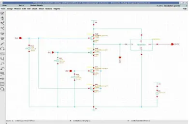
Fig. 3.3 Basic domino AND gate schematic simulation.181
Copyright © 2017. Vandana Publications. All Rights Reserved.
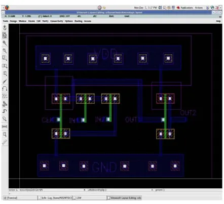
Fig. 3.5 Basic domino AND gate-Extraction of Layout.182
Copyright © 2017. Vandana Publications. All Rights Reserved.
After simulating this circuit at different technologies the following observations were made.
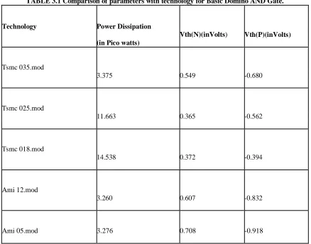
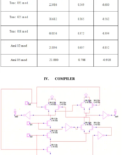
TABLE 3.1 Comparison of parameters with technology for Basic Domino AND Gate.
Technology Power Dissipation
Vth(N)(inVolts) Vth(P)(inVolts) (in Pico watts)
Tsmc 035.mod
3.375 0.549 -0.680
Tsmc 025.mod
11.663 0.365 -0.562
Tsmc 018.mod
14.538 0.372 -0.394
Ami 12.mod
3.260 0.607 -0.832
Ami 05.mod 3.276 0.708 -0.918
From the above table it is observed that with the down scaling of technology, more power is consumed. Specifically, the need to decrease the dynamic power consumption forces us to use a lower power-supply voltage. This in turn necessitates the reduction of threshold voltage to maintain the performance with the associated increase in sub threshold leakage current. So, a properly sized PMOS keeper must be used to compensate for this leakage. It will be found that the speed, which is the major advantage of domino logic compared to other logic styles, will degrade with CMOS technology scaling due to the contention current of the keeper
3.2 PMOS Keeper To Compensate Charge Lost:
However, it has been assumed in the previous paragraph that there is no leakage of the charge stored on the dynamic node capacitor, CL. In practice, however, there are various sources of leakage during the evaluation
183
Copyright © 2017. Vandana Publications. All Rights Reserved.
Fig. 2.9 Basic domino AND gate-using PMOS-keeper schematic implementation.
184
Copyright © 2017. Vandana Publications. All Rights Reserved.
After simulating this circuit at different technologies the following observations were made.
TABLE 3.2 Comparison of parameters with technology for Basic Domino AND Gate using PMOS Keeper.
IV.
COMPILER
185
Copyright © 2017. Vandana Publications. All Rights Reserved.
Domino NOR and OR gates186
Copyright © 2017. Vandana Publications. All Rights Reserved.
4.2.Domino logic 4 input OR gateOutput waveform of Domino logic 4 input OR gate
187
Copyright © 2017. Vandana Publications. All Rights Reserved.
Domino diode footed OR gate output waveform4.4 Domino scheme 8 OR logic
188
Copyright © 2017. Vandana Publications. All Rights Reserved.
4.5. Proposed scheme OR logic189
Copyright © 2017. Vandana Publications. All Rights Reserved.
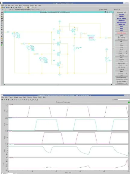
Domino Octal to binary encoderDomino Octal to binary encoder output waveform
V.
CONCLUSION AND FUTURE
SCOPE
In this paper we have proposed high speed low PDP domino logic circuit, which exhibits some noise tolerance at the output node. Simulations are done using
190
Copyright © 2017. Vandana Publications. All Rights Reserved.
binary encoder is designed and simulated with proposed technique.
REFERENCES
[1] John P. Uyemura “CMOS Logic circuit
Design”Springer International Edition, 2005.
[2] H.L. Yeager et al, “Domino Circuit Topology”, U. S. Patent 6784695,Aug. 31, 2004.
[3] Krambeck, R.H., Lee.C.M., and Stephen Law.H.F., “High- speed compact circuits with CMOS”, IEEE J. Solid-State Circuits , 1982, 17, (3), pp 614-619.
[4] Oklobdzija, V.G., and Montoye, R.K., “Design performance tradeoffs in CMOS domino logic “.Proc. IEEE Conf. on Custom Integrated Circiuts, May 1985, pp.334-337.
[5] Oklobdzija, V.G., and Montoye, R.K., “Design performance tradeoffs in CMOS domino logic “., IEEE J. Solid-State Circuits 1986, 21,(2), pp 304-306.
[6] Mohmoodi-Meimand H, Roy K., “ Diode-footed domino: a leakage tolerant high fan-in dynamic circuit design style” , IEEE Trans. Very Large Scalr Integr. Syst., 2004, 51, (3), pp. 495-503.
[7] Frustaci F.,Corsonellop., Cocorullo G., “A new noise tolerant dynamic logic circuit design”, IEEE Ph.D. Research in Microelectronics and Electronics, PRIME 2007, Bordeaux, France, July 2007, pp 61-64.
[8] Preetisudha Meher, Kamala Kanta Mahapatra, “A technique to increase noise tolerance in dynamic digital circuits”, Asia Pacific conference in post graduate Research in Microelectronics and Electronics (PRIMEASIA), December 2012, pp229-233
[9] F. Mendoza-Hernandez, "Design techniques to enhance noise tolerance in cmos digital dynamic circuits," Phd Thesis, INAOE, Puebla, Mexico,Aug. 2003.