Doctoral School in Materials, Mechatronics and Systems Engineering
Flash Sintering of Alumina-based Ceramics
Mattia Biesuz
April 2017
XXI
X
c
y
c
F
LASH
S
INTERING OF
A
LUMINA
-
BASED
C
ERAMICS
Name
E-mail: [email protected]
Approved by:
Prof. Vincenzo M. Sglavo, Advisor Department of Industrial Engineering University of Trento, Italy
Ph.D. Commission:
Prof. Giandomenico Sorarù, Department of Industrial Engineering University of Trento, Italy.
Prof. Rodrigo Moreno, Instituto de Ceramica y Vidrio Spain.
Prof. Enrico Bernardo,
Department of Industrial Engineering University of Padova, Country.
University of Trento,
Department of Industrial Engineering
University of Trento - Department of Industrial Engineering
Doctoral Thesis
Mattia Biesuz - 2017
Abstract
Flash sintering is an electrical field-assisted
consolidation technology and represents a very novel technique for producing ceramic materials, which allows to decrease sensibly both processing temperature and time. Starting from 2010, when flash sintering was discovered, different ceramic materials with a wide range of electrical properties have been successfully densified.
Up to date, the research on flash sintering has been mainly focused on ionic and electronic conductors and on semiconductor ceramics. In the present work, we studied the flash sintering behavior of a resistive technical ceramic like alumina also in the presence of magnesia silicate glass phase typically used for activating liquid phase sintering. The materials were studied by using different combinations of electric field and current density. Physical, structural and microstructural properties of sintered samples were extensively investigated
by Archimedes’ method, SEM, XRD, XPS and pholuminescence
spectroscopy. Light emission and electrical behavior during the flash process were studied,as well.
The results point out the applicability of flash sintering to alumina and glass-containing alumina using electrical-field in excess of 500 V/cm, allowing an almost complete densification at temperatures lower than 1000°C. Different densification mechanisms were pointed out in the two systems, namely “solid state flash sintering” and “liquid phase flash sintering” for pure alumina and glass containing alumina, respectively. The glass addition allows a significant reduction of the current and power dissipation needed for densification, by promoting liquid phase sintering.
gets partially reduced during DC-flash sintering experiments is supported by several experimental findings.
Finally, strong affinities between flash sintering and other physical processes, like dielectric breakdown, were pointed out.
Table of contents
Abstract ... i
Table of contents ... iii
1 Introduction ... 9
1.1 Sintering of ceramics ... 9
1.2 Flash sintering principles ... 11
1.3 Proposed mechanisms for flash sintering ... 18
1.4 Flash sintering: Phenomenology ... 22
1.4.1 Thermal runaway and Joule heating ... 22
1.4.2 Sintering and microstructures ... 33
1.4.3 Electrical behavior ... 40
1.4.4 Light emission ... 42
1.4.5 Textures and new phases ... 44
1.5 Materials densified by flash sintering ... 45
1.6 Flash sintering and related technologies... 48
1.6.1 Flash sintering of tape casted layers ... 48
1.6.2 Travelling electrodes ... 49
1.6.3 Hyper-flash and double flash ... 49
1.6.4 Contactless Flash Sintering (CFS) ... 50
1.6.5 Flash Spark Plasma Sintering (FSPS) ... 51
1.6.6 Field-Assisted Sintering Technique (FAST) ... 53
1.6.7 Flash reactions ... 54
2 Aim of the work ... 56
3 Experimental procedures ... 57
3.1 Materials and samples preparation ... 57
3.2 Experimental set-up n. 1 ... 59
3.3 Experimental set-up n. 2 ... 60
3.4 Conventional Sintering ... 62
3.5 Characterization ... 62
3.5.1 Microstructure ... 62
3.5.2 Phase analysis ... 62
3.5.4 XPS 63
3.5.5 Photoluminescence spectroscopy ... 63
4 Results and Discussion ... 64
4.1 Flash sintering of alumina ... 64
4.1.1 Densification behavior and microstructural evolution ... 64
4.1.2 Electrical behavior ... 78
4.1.3 Photoemission during Flash Sintering ... 106
4.1.4 Flash Sintering and Dielectric Breakdown ... 115
4.1.5 Electrode Material Effect ... 123
4.2 Flash sintering of glass-containing alumina... 130
4.2.1 Densification behavior and Microstructural Evolution ... 130
4.2.2 Electrical behavior and onset for flash sintering ... 141
5 Conclusions ... 157
6 Future Perspectives ... 159
List of abbreviation and acronyms ... 160
References ... 161
Scientific Production ... 175
Participation to Congresses, Schools and Workshops ... 177
1 Introduction
1.1 Sintering of ceramics
Ceramics are inorganic, non-metallic materials characterized by unique combination of physical, mechanical, thermal and functional properties. In general, they are lighter and harder than metals, more resistant at high temperatures, to creep, to wear and to corrosion. Despite their inherent brittleness, they can be toughened and are characterized by high stiffness and mechanical strength, finding many structural applications, from buildings to refractories, from aerospace industry to cutting tools etc.. In the last decades great interest has also been risen by functional ceramics for they outstanding piezoelectric, electrical, magnetic and biological properties[1,2]. Different processing routes have been developed for obtaining ceramic materials; for example, coatings can be obtained via CVD, PVD, TRD, sputtering methods; porous ceramics can be processed from sol-gel, xerogel, aerogel techniques. However, the production of bulk ceramic is much more complicated. In fact, ceramics are brittle, hard and characterized by high melting temperature thus they can not be casted (with the exception of some ZAS refractories) or easily machined by plastic deformation of cheap removal. For all these reasons, ceramic materials manufacturing involves powder shaping and a high temperature powder consolidation process, called sintering[3]. The firing process is crucial when discussing about ceramics; in fact, controlling the firing parameters (time, temperature, atmosphere) it is possible to change the final properties of the sintered body: relative density, mechanical strength, toughness, grain size, electrical, magnetic and functional properties[2,3].
Sintering is a process based on diffusion, and therefore needs high temperatures and quite long time (in the order of hours) [3]. Indeed, the firing temperature depends from the composition of the material; it ranges between 800 - 1300°C for traditional ceramics (bricks, porcelain, earthenware…) but could reach temperature up to 1900°C for several advanced ceramics. Therefore, sintering is characterized by high costs, which are both economic and environmental.
consumption for different class of ceramics is summarized. In all the cases, some MJ are needed for each kg of final product as shown in Table I. One should consider that the main part of the energy is consumed during the sintering process; i.e. considering the production of MgO refractory 3.0-6.3 MJ/kg are needed only for firing, while the overall energy consumption lays between 3.5-7.15 MJ/kg [4]. Today the larger part of energy required for the firing process is provided by the combustion of “natural gas, liquefied petroleum gas (propane and butane) and fuel oil EL …; while heavy fuel oil, liquefied natural gas (LNG), biogas/biomass, electricity and solid fuels (e.g. coal, petroleum coke) can also play a role as energy sources for burners”[4]. The energy cost of natural gas is around 0.1 €/kWh, that means that the firing process requires 0.05 - 0.2 € for kg of ceramic. These values seems to be quite low but one should consider that only in Italy the refractory production in 2011 was 486,336 tons and the production of tableware was 13,200 [5]. Hence, the energy cost for refractory production in Italy can be estimated in the order of several millions of euros. This value is only referred to the energy cost, the actual cost of the firing process should account also for plant cost and maintenance. Typically the price of a tunnel kiln for porcelain/tableware is in the order of 500,000-1,000,000 €.
Therefore, it is crucial, both for economic and environmental reasons, to explore new ways for reducing sintering time and temperature of ceramics. Among the different possibilities field-assisted sintering in general, and flash sintering in particular, represents a very promising route.
Table I: Energy consumption for manufacturing different class of ceramics
[4].
Material Energy Consumption [MJ/kg]
Roof Tiles 1.90 - 2.95
Masonry Bricks 1.50 - 2.50
Porcelain Tableware 4.50 - 7.00
Vitrified Clay Pipes 6.19 - 7.86
1.2 Flash sintering principles
Flash Sintering (FS) is a consolidation technology which allows to reduce the temperature needed for densifying ceramics by hundreds of degrees [6,7]. In some cases the reduction of the firing temperature approaches 1000°C[8,9]. Additionally, in FS experiments the densification occurs in few seconds (or minutes) much more quickly than in the conventional processes, which usually require hours. The reduction of the processing times and temperature by FS is, in general, larger than what can be obtained using other innovative sintering technologies, like SPS or hot press (Figure 1).
Figure 1: Typical time and temperature for sintering YSZ using different technologies. Taken from [10].
cannot be obtained via conventional processes. Additionally, the short treating time allows to obtain dense ceramics with very limited grain coarsening.
Flash sintering is a very novel sintering technique, the first paper on this argument having been published in 2010 by Cologna et al.[6]. FS belongs to the family of Field-assisted Sintering Technology (FAST), where the combination of electric field/current application and temperature allows a rapid densification.
FS presents some peculiar characteristic when compared with other field-assisted routes like Spark Plasma Sintering (SPS). The main difference is that in FS process the current is forced to flow within the specimen whereas in SPS the sample is contained in a graphite die which, being usually more conductive than the ceramic, is responsible for the current flow. Hence, the heat generation mechanism is pretty different in FS and SPS. In SPS the die is heated by Joule effect, then the sample is heated by radiation/conduction from the die. Conversely, heat generation within the green specimen takes place in FS, as a result of the current flow. For this reason the heating rate involved in the two processes are pretty different,up to 103 °C/min for SPS, in the order of 104 °C/min for FS [13]. Actually, the current flow within the specimen during sintering can not be considered the only discriminant characteristic for defining flash sintering. In fact, also in many SPS processes of metal powder the current mainly flow within the metal (often more conductive than the graphite die). Therefore, we need to improve the definition of FS.
An accurate analysis of the scientific literature on this topic allows to define flash sintering as a very rapid sintering phenomenon (few seconds/minutes) accompanied by a current flow within the sample and by the so called “flash event”.
The flash event is characterized by three phenomenological effects:
i. The sample is quickly heated by an internal Joule effect[13–15]; ii. The material shows a transition from insulator to conductor-like[6–8,16]; iii. The sample starts to emit light[17–20].
The flash event is not strictly related to sintering and it can be observed also in dense specimens. FE has been reproduced also in different pre-sintered materials with different level of densification (SiC [23], LSCF[24], YSZ [9,25] …). Of course, we can not talk of flash sintering in this case since the material is already dense. Nevertheless, if FE is reproduced on a green body, a very rapid densification occurs and the process can be identified as flash sintering.
Therefore, we can state that ”Flash sintering is a field assisted sintering technique, characterized by a current flow within the specimen and showing a very rapid densification, a drop of electrical resistivity, a quick internal heating of the specimen by Joule effect and a strong light emission”.
The experimental set up for flash sintering is not complex and expensive; it is usually constituted by four main parts(Figure 2):
i. Electrical furnace; ii. Power source; iii. Multimeter;
iv. Displacement sensor.
monitored by measuring the sintering shrinkage using a displacement sensor (like an LVDT[26]) or making a video with a CCD camera (Figure 2).
Different sample shapes have been employed in FS experiments. The specimens used in the first FS experiments were characterized by a dog bone shape with two holes at the opposite side of the specimen. The electrodes are forced within these holes. This shape is quite complex and find limited technological applications; nevertheless, this is the best choice for studying the process. In fact, the dog bone shape reduces many problems observed during FS like current concentrations. So, the samples result homogeneous in their cross-section and the conductivity evolution can be easily studied. The second geometry used in flash experiment is bar-like. In this case the metallic wire is wrapped around the external part of the green specimen. The third used geometry corresponds to cylindrical pellets. The electrodes are often constituted by metallic disks or grids pushed in contact with the pellet faces. Also in this case the application of a conductive paste can be very effective for reducing sparkling at metal/electrode interface or for improving the homogeneity of the sintered body. Nevertheless, especially if stocky geometry are used (high diameter/height ratio) current concentrations are very likely to be formed leading to a non-homogeneous sintering process[27].
Figure 2: Two possible experimental set up for flash sintering experiments: the sintering can be monitored by a CCD camera (a) or by an LVDT sensor (b).
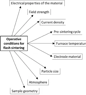
Figure 4: Process parameters that influence the flash sintering behavior.
Flash sintering experiments can be carried out applying the main process parameters (T, E, J) in different ways. The two most common experiments are reported in Figure 5.
current flow also increases the specific power dissipation (w) within the ceramic that can be calculated as:
(1)
Now, since the system during the incubation is working in current control, we can calculate was:
(2)
where ρ is the electrical resistivity of the material. Since, in many ceramics ρ is decreasing with temperature (following an Arrhenius-like behavior), during the incubation of FS the power slowly increases. Exceptions are represented by metallic like ceramics, among them WC, HfB2, MAX phases et cetera.
At a certain onset temperature an abrupt drop of electrical resistivity is observed and the current rises. The system switches from voltage to current control, reaching the maximum power dissipation. This is referred as the flash event or II stage of flash sintering[19]. During this stage the highest power dissipation are reached and the sample undergo to a thermal runaway of Joule heating. In this stage the densification starts and extremely higher sintering rates are obtained. It is to underline that the onset temperature for FS is in almost all the cases much lower than the conventional sintering temperature; thus, resulting in an anticipate sintering phenomenon. After that the system reaches the current limit, the field decreases reaching an equilibrium condition. When the field is stabilized the III stage or steady stage of FS begins[19]. Now the system is working in current control; therefore, the specific power dissipation (w) can be written as:
. (3)
Figure 5: Electric field (E) and current (J) evolution during constant heating rate (a) and constant furnace temperature, Tf, (b) flash sintering experiments.
Figure 5(b) shows the second most used experimental set up for FS. In this case the furnace is at a constant temperature. Once that the power supply is switched on the current start to flow and, even if the furnace temperature is constant, J progressively increases with time. This behavior can be observed only if appropriate field strength is used: if the field is too low J remains constant. Also in this case an abrupt drop in electrical resistivity is observed and the flash event takes place. Therefore, it is possible to define again three stages: first the system works in voltage control and the current slowly increases, then the flash event is observed, finally the system reaches a new equilibrium in current control. When the isothermal flash experiments are conducted the most significant parameter to define the material behavior is the incubation time, which is the time needed for the system to switch from voltage to current control. The incubation time is of course related to furnace temperature and applied field [28], this will be discussed in the next sections.
1.3 Proposed mechanisms for flash sintering
interest are mainly technology-driven; an industrial application of FS would allow a drastic reduction of sintering costs, energy consumption and CO2 emissions. Nevertheless, being the process very “rich” and multidisciplinary (involving sintering, light emission, electrical properties, new phase formation, textures, non-conventional microstructures…) also a lot of scientific interest has been risen with the aim to interpret and explain the phenomenon. With this purpose different mechanisms for flash sintering have been proposed.
All mechanisms start from the assumption that for explaining flash sintering one should explain both charge and mass transport. Charge transport can be either ionic or electronic, depending from the structure of the material, its purity or from temperature. However, it seems reasonable that the extremely high heating rates obtained during the flash event are unlikely to be due to ionic conduction alone. Probably, a dominant electronic contribution to Joule heating can be pointed out, as a result of a massive electronic scattering. Conversely, mass transport involves diffusion and atoms movement from the surface with positive to negative curvature. Probably, the simplest explanation for flash sintering is based just on Joule heating: the sample is heated by the current flow and for this reason both electric conduction and diffusion are enhanced. At this point the question is: “Is the real sample temperature upon FS high enough for justifying a such rapid densification? Is the sample temperature enough high for justifying the drop of electrical resistivity?” These are still opened questions and will be more in detail discussed point by point in the next sessions.
stress would be ~ 27 MPa [30], this stress is indeed higher than the sintering stresses and comparable to the load usually applied during SPS processes. This would provide an additional driving force for densification.
The formation of a local liquid film or temperature gradient between GB and bulk are a very attractive hypothesis. In fact, they could also explain some microstructures obtained via flash sintering: the ceramic can be sintered up to nearly full density with submicrometric grain size[6,32–34]. In addition, previous works have shown that in monolithic YSZ specimen the application of a weak DC electric field results in a retarded grain coalescence[35]. Ghosh et al. have proposed that if the grain boundary is hotter than the surrounding region this would lead to a minimum of the interfacial energy ( ). This could be explained considering the Gibbs energy
associated to the grain boundary:
(4)
where and the excess of enthalpy and entropy associated to the GB. Thus, if the temperature is higher at the GB a minimum in the interfacial energy is achieved. If the grain boundary moves, towards colder region would increase in
this reduces the driving force for grain growth.
The effect of a liquid film formation on grain coalescence was studied by Narayan [36]. He demonstrated that in case of selective melting of the grain boundary the driving force for grain growth is reduced almost to zero. This should inhibit all grain coalescence phenomena.
differences between grain boundary and bulk are not the crucial mechanism behind flash sintering.
The third mechanism involves the formation of Frenkel pairs within the grains during the flash event[6,38–40]. Also, a thereof model based on nucleation theory has been developed in order to explain the incubation time in isothermal FS experiments. In this model embryos of material with high dielectric constant are thought to be formed under E field application, as a result of dipoles vacancy/interstitial associated with Frenkel defects [41]. In this way the electric field provides the driving force for nucleation and a critical radius for the embryos, above which nucleus can growth, can be calculated in nanometric – submicrometric scale [41].
In the next sections we are going to describe more in detail the different phenomenological effects observed during flash sintering are described in detail and links with the proposed mechanisms are provided and discussed.
1.4 Flash sintering: Phenomenology
1.4.1 Thermal runaway and Joule heating
The thermal runaway is always occurring during the flash event and allowing an abrupt heating of the ceramic due to internal heat generation. It was calculated that during the flash event the heating rate could approach 104 °C/min [13]; nevertheless, this value depends on the maximum specific power dissipation set during the experiments, the material specific heat and other process parameters (sample shape, mass…).
line represents the power dissipated by Joule effect as a function of the sample temperature ( ). This curve is rising with temperature; in fact, being the system in voltage control during the incubation of FS the electrical power dissipation ( ), assuming Arrhenius conduction and an homogeneous sample temperature, is:
( ) (5)
where W is the power dissipation, V the sample volume, the pre-exponential constant for resistivity, Q the activation energy for conduction, R the universal gas constant.
The blue lines represent the heat dissipated from the sample by radiation (Wout) at different furnace temperatures (TF). Indeed, also this curve rises with TS; in fact, higher the temperature difference between the sample and the atmosphere higher will be the heat exchange. If the temperature is enough high one can assume that all the heat is exchanged by radiation and so it is possible to write:
( ) (6)
where S is the sample surface, the Stefan-Boltzmann constant and the emissivity. According to Eq. 6 ramping the furnace temperature the curve moves to the right in the plot in Figure 6(a). If the furnace temperature is low (dashed line in figure) and curves presents an intersection which represent an equilibrium condition and FS cannot be reproduced. However, increasing TF the two curves becomes tangent; in this case the power that is consumed by Joule effect cannot be dissipated by the sample (being plot always above ) and this represent the onset for FS. Therefore, the sample undergo to an uncontrolled heating process, which is at the base of the flash event. The relation between the onset field/temperature in constant heating rate experiments results monotonical; being the sample treated with larger field flash sintered at lower temperatures[8,57]. This is due to the fact by increasing E the in
temperature. The experimental relation between onset temperature for FS and electric field is reported in Figure 7(a) for 8YSZ. One can observe that, by increasing E, a drastic reduction of sintering temperature can be obtained.
Similar consideration can be done for isothermal flash experiments. In this case
plot do not change its position (being the furnace temperature constant); but increasing E the curve moves upward and so, once again, an onset condition can be determined. Indeed, the incubation time depends from the applied field and furnace temperature, as shown in Figure 7(b). Increasing E the area between and becomes larger and this means that the net power absorbed by the sample rises. Therefore, increasing E the sample would undergo to a more rapid heating, reducing the incubation time. An analogous behavior can be obtained increasing the furnace temperature at which the experiments are carried out: increasing TF it becomes more “difficult” to dissipate the internal heat generated by Joule effect.
Figure 7: Relation between onset flash sintering temperature and electric field (a) [8]and between incubation time an the applied field for different furnace temperature (b) for YSZ[28].
The onset condition for thermal runaway is not only depending on the applied field but it is also a function of the electrical properties of the tested material, the more conductive specimens being flash sintered at lower temperatures. This behavior is quite well known from the early flash sintering experiments and it can be demonstrated just comparing the flash temperature for different materials [6,33,39,58–60]. Such relation is due to the fact that the more conductive specimens during the incubation of FS are characterized by higher power dissipation (the system is working in voltage control); in this way, the red curve in Figure 6 would shift upward and the onset condition can be easily reached.
More recently, Pereira da Silva et al.[52] and Dong et al. [53,54] developed more sophisticated models for the thermal runaway. In particular Dong et al. calculated the relation between the onset field and temperature as [54]:
(
)
(7)
where Q is the activation energy for conduction, Ton the onset temperature for flash sintering at a given field (E) and A is a constant depending from the sample geometry/heat exchange and can be empirically calculated. Eq. 7 has been proved to provide a quite good approximation of the many experimental results obtained in constant heating rate flash sintering experiments[54].
environment, but significant heat loss could take place by conduction through the metallic electrodes. They calculated the heating rate of the specimen as:
( ( ) ( )) (8)
where C is the sample heat capacity for unit of volume, r the sample radius, h the specimen height, and are the are the heat transfer coefficients at the flat surface (in contact with the electrode) and side surface, respectively.
The key point that deserve to be underlined from Eq.8 is that the heating rate obtained during the incubation of the flash event is dependent from sample geometry; i.e. larger samples (high value of r of h) being characterized by higher heating rate using the same field strength. This result is in perfect agreement with many experimental findings. In fact, it has been shown that the flash event can be reproduced using lower incubation times in large specimens (Figure 8(a)) [56]. Additionally, it was demonstrate that, when working with very thin samples (in the order of few mm), the onset temperature for FS could increase of hundreds of degrees with respect to the traditional dog bone geometries[61].
The strong relation provided by the thermal runaway model between sample conductivity and onset condition (field/temperature) for flash sintering can explain also other experimental results:
ii. Although flash sintering is mainly a pressure-less technique flash-sinterforging experiments have also been carried out. Francis et al. showed that an external pressure application (1.5 - 12.0 MPa) can reduce the onset temperature for the flash event(Figure 8 (c)) [63]. They explained this effect as a result of local field enhancement due to electro-chemo-mechanical effect. However, an external pressure application could enhance the quality of the particle/particle contact and reduce the temperature needed for particle welding; thus, allowing an increase in electrical conductivity and reducing the onset temperature for FS. iii. The sintering atmosphere (oxygen partial pressure, reducing potential…)
can change the defect population in oxide ceramics. This has an influence on electrical conductivity and so also on the onset condition for flash sintering. The atmosphere effect on flash sintering on ZnO was studied by Zhang et al. [64]. They showed that the onset condition for FS can be reduced of hundreds of °C using Ar or Ar/H2 atmosphere when compared with air (Figure 8(d)).They attributed this behavior to an higher conductivity showed by ZnO in reducing atmosphere[64]. Nevertheless, the ionization potential of Ar is much lower than air (N2/O2). Therefore, it is also possible to suggest a partial contribution of an interparticle plasma formation, which rises electrical conductivity. Further experiments in inert and high dielectric strength atmosphere (i.e. N2) would be needed for an accurate and definitive understanding of atmosphere effect on flash sintering.
Figure 8: Sample length effect on incubation time for FS in Al2O3/YSZ composites (a)[56]. Effect of particle size (b)[62] and applied pressure on onset FS temperature for YSZ[63]. Onset temperature dependence from sintering atmosphere in ZnO (d) [64].
Figure 9: Relation between onset temperature for FS and applied field for 8YSZ in AC and DC treatments.[57]
So far we analyzed Joule heating as a trigger for the flash event and we focused our analysis on what is happening when the system is working in voltage control. Now, we describes what is going on when the current limit is reached. At this point, the power dissipation peak is observed and it is equal to the voltage limit times the current limit. The product of these two values gives the maximum power dissipation that can be obtained and so it is strictly related to the maximum heating rate achievable by the system. Then, being the system in current control, the power dissipated by Joule effect can be written as:
( ).
(9)
condition when the electrical power is equal to the heat dissipated by radiation toward the environment (Figure 10).
This new equilibrium is reached at a sample temperature higher than that at which the power peak is observed. Therefore, also after the current limit reaching the sample is still heated. This is due to the fact that after the power peak the still is higher than . Nevertheless, the difference between the two power decreases with sample temperature (TS), so the heating rate progressively decreases and the temperature approaches the equilibrium one. As a result of this heating process after the current limit reaching the resistivity of the material decreases and it is responsible for the decrease of E as reported in Figure 5. When E is stabilized and the equilibrium temperature is reached the third stage of FS, also known as steady stage begins.
Figure 10: Qualitative power dissipation plot during the different stages of flash sintering.
A correct estimation of the real sample temperature during the steady stage of flash sintering is crucial: it would allow to clarify if the temperature increase due to Joule effect is or not the only reason at the base of a so rapid densification and electrical resistivity drop.
A first analytical attempt to determine the sample temperature during FS was carried out by Raj [65] . He provided an analytical expression for calculate the sample temperature assuming an homogeneous power dissipation in sample gage section and that the heat is only exchanged by radiation. This allows to write that:
( )
(10)
where S is the sample surface area and can be easily measured by multimeter. Being this relation referred the heat exchanged from the surface by radiation it allows to calculate the surface sample temperature and do not give direct information of the temperature in the core. Although Eq. 10 is based on some approximations and the value of the emissivity (ε) should be a priori estimated, this has provided in many cases a good approximation of the real sample temperature during FS of dog bone specimens. In fact, the results obtained using Eq. 10 were successfully compared with sample temperature measurement by experimental technique[17,19,63]. Different experimental attempts were for measuring the specimen temperature during the steady stage of flash sintering:
i. Park et al. measured the sample temperature by in situ impedance spectroscopy[66]. However, this method is based on the assumption that during the flash event no unconventional conduction mechanisms are activated; hence, it would be possible to compare the impedance measured during the flash with the conductivity extrapolated in conventional conditions.
this kind of measure, especially assuming that often the emissivity could change with temperature[70].
iii. Probably the more accurate measure of sample temperature during FS has been done by XRD[17,71]. In fact, the XRD peak position depends from the cell parameter which, with an appropriate calibration can be related to the ceramic temperature.
iv. When reproducing the flash event on dense specimen the sample temperature can be estimated from the thermal expansion[72]. This method is not working for flash sintering, where the sintering shrinkage would hide the thermal expansion.
The last point that deserves to be discussed about Joule heating regards the temperature distribution homogeneity within the specimen. If we assume that heat is exchanged by radiation from the surface it would be reasonable that the hearth of the specimen was hotter than the surface. Nevertheless, no microstructural evidences of such e phenomenon (i.e. densification or grain size gradients) have been reported for dog-bone specimen. Lebrun et al. investigated the temperature distribution in dog bone geometry (cross section: 1.3x0.65 mm2) via XRD[71]. They observed in YSZ that a broadening of diffraction peak width related to temperature gradients can be observed only if the power peak exceeds 1000 mW/mm3; this value is higher than what usually needed for FS of zirconia ~ 500 - 1000 mW/ mm3. If the
considering both temperature gradients in radial and axial direction due to the heat loss through sample surface and metal electrodes, respectively. Their analytical solutions have suggested that some temperature gradients can be present during the steady stage of flash sintering of cylindrical pellets[74].
1.4.2 Sintering and microstructures
The sintering process is conventionally divided into three main stages. According to Rahaman[3], in the first stage the particles get welded together via interparticle neck formation. This stage is activated at relatively low temperature and it is usually based on surface diffusion or evaporation/condensation mechanisms. At such temperatures a very moderate densification can be achieved and the distance between particles center remains substantially constant. It is assumed that the stage finishes when a relative density of ~65% is reached, or when the radius of the interparticle necks
reaches 40-50% of the particle radius.
At higher temperature bulk and grain boundary diffusion get activated and the second stage of sintering starts, leading to densification up to ~90%. The
densification is accompanied by a strong shrinkage of the material based on the fact that the particle centers get closer. In this stage the pores are still quite continuous and they reaches their equilibrium shape forming the dihedral angles. When the pores get isolated at the grain corners the third stage of sintering begins, allowing an additional densification and shrinkage.
Therefore, when we discuss of the electric field effect on sintering we can divide the argument in two main parts:
i. First, we can analyses the field effect on neck formation (I stage of sintering)
ii. Second, we can analyses the field effect on densification (II-III stage of sintering)
diffusion. For these reasons it seems that FS can be more correctly classified as Electric Current-Assisted Sintering (ECAS) rather than a Field-Assisted Sintering. Conversely, a very huge effect of electric field/current application can be observed when the flash event is reproduced, allowing a very rapid densification (few seconds) at very low furnace temperature[6–8,24,68,76]. Therefore, the electric field/current effect on the I stage of sintering is in general very moderate, while it becomes more relevant when describing the II and II stage. In fact, until a relevant current density is reached the field effect are limited.
At this point a good question is: “Is the Joule heating observed during the flash event enough for justifying a so rapid densification?”. A definitive answer regarding this point has not been achieved and unanimously accepted yet by the scientific community, also considering how difficult is to obtain a precise measure of sample temperature during the flash event.
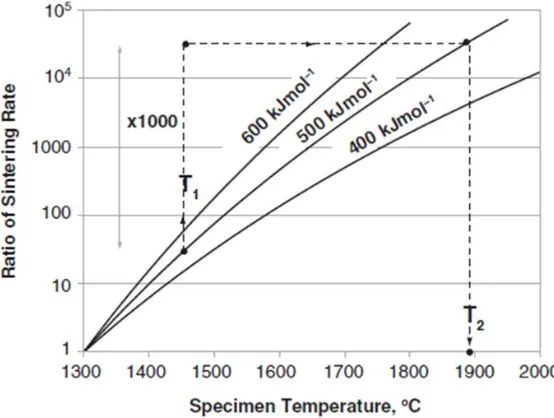
What is pretty sure is that at least a partial contribution of Joule effect on densification can be pointed out. However, Raj showed that the temperature reached during flash sintering are much lower when compared with what would be expected from the measured sintering rate during flash sintering[65]. In particular he showed that 3YSZ during FS is densified in ~3.6 s, while conventional sintering processes
requires soaking time of ~1 h (3600 s) at 1450°C. This means that during the flash
event the sintering rate is ~1000 times higher than in conventional processes.
Figure 11: Sintering rate as a function of sample temperature using different activation energy for densification. T1 is the specimen temperature estimated using Eq.10; T2 is the temperature needed for justifying the observed sintering rates[65].
On these bases, being the sintering rate proportional to the defect population, a mechanism based on field-induced Frenkel pairs formation was developed[6,38– 41,62]. However, up to now quite poor experimental evidences have been recorded supporting this theory. Additionally, what it seems is that the enhanced sintering rates are more current-induced than field-induced. In fact, until the current is low there are no significant field effect on sintering, like it has been pointed out by Cologna et al. in the early stages of FS[75]. Whereas, during the flash event when the current starts to flow, and the field decreases, differences between the conventional sintering and flash sintering can be pointed out, even considering Joule heating [65].
using DC field. The possibility of the formation of a partially reduced oxide during DC flash sintering experiments has been for the first time pointed out by Muccillo et al. in 2011[47] and it has been in detail discussed by Down in 2013 [9]. Narayan states that the partial reduction of the oxide would lead to the formation of discharged oxygen vacancies; that are characterized by a lower activation energy for diffusion[29]. Additionally the reduction of the oxidation state of cations can influence their mobility during flash sintering[48,49]; the result is coherent also with grain growth enhancement measured in reducing atmosphere [50,51].
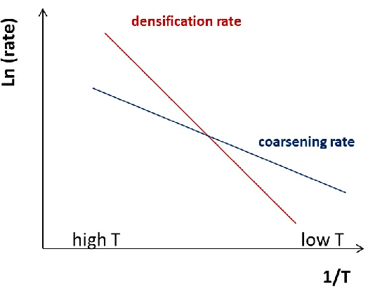
One last point deserves to be analyzed when discussing about densification during flash sintering. This point is focused on the concept that the sintering rate during flash sintering cannot be easily compared with conventional processes. This is due to the fact that the heating rates are completely different: according to Grasso et al. the heating rate during the flash event could reach 104 °C/min[13], ~ 3 order of magnitude higher than in conventional process.
Figure 12: Qualitative behavior for sintering rate and grain coarsening under the assumption that the activation energy for the latter is lower. One can observe that at high temperature densification is enhanced, while at low temperature grain coarsening is more fast. In this case we assume that the sample temperature is homogeneous (grain boundary and grain core are at the same temperature).
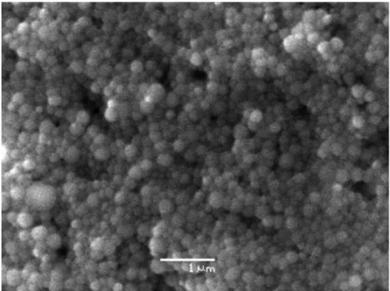
Figure 13: SEM micrograph of a dense flash sintered GDC specimen with sub-micrometric grain size. Taken from [34].
Conversely, Naik et al. studied the effect of a prolonged dwelling time in the III stage of FS on the microstructure evolution of alumina, zirconia and composites [82]. They suggested that during the flash event the activation energy for grain growth do not change significantly; nevertheless, the grain growth is enhanced compared with conventional sintering. Thus, they suggested that this could be related to an increase of defect population. Also other authors observed abnormal grain growth in field-assisted processes [83].
oxidation state of the cations. This would decrease the energy barrier for diffusion and enhance, locally, grain boundary mobility[48,49].
Figure 14: SEM micrograph on a 8YSZ flash sintered specimen showing a strong microstructure asymmetry (24 h at 1250°C, 50 A/cm2). Taken from
[49].
Surprisingly, completely different results were reported by Zhang et al. [15] who observed abnormal grain growth at the anode when working with ZnO [15]. They explained such a behavior assuming that cation vacancies could be formed at the anode according to:
→
(11)
→
(12)
These reactions increase the cation vacancy population at the anode and, being cation diffusion controlling grain growth rate, this results in a faster grain coarsening. However, in a recent work carried out on flash sintered zinc oxide it has been shown, via catholuminescence, that the main defect introduced by flash sintering in the crystal structure are anionic vacancies [84]. Zhang and co-workers also reported that this asymmetry is much reduced when a liquid phase is added for promoting sintering[15].
spectroscopy. However, the reported data are contradictory. Du et al. reported that both bulk and grain boundary impedance response are similar in conventional and flash sintered specimens[85]. M’Peko et al. suggested that in flash sintered sample the grain boundary thickness is lower and characterized by higher defect concentration than in conventional materials [86]. Finally, they have shown that the specific grain boundary conductivity is higher in flash sintered specimen. Results consistent with those provided by M’Peko were observed also by Liu and coworkers[87]. These results could be explained based on the theory of Frenkel pairs nucleation. However, the partial reduction of the oxide, increasing oxygen vacancy population, is also coherent and probably it provides a better explanation. In fact, Du et al. have carried out FS using AC field which do not lead to any reduction, so they have found strong affinities between flash sintered and conventionally sintered YSZ. Conversely, M’Peko, Liu and coworkers carried out a DC flash sintering experiment; which lead, even in short treating time to a modification of the material structure.
1.4.3 Electrical behavior
The electrical resistivity drop is one of the main characteristic of the flash event. This results in a non-Arrhenius behavior when plotting conductivity or electrical power dissipation vs. the inverse of furnace temperature. This behavior was been observed on different materials as shown in Figure 15.
The Arrhenius behavior in Figure 15 is represented by the region where the power dissipation follows a straight line (low temperature, right side of the plots); however, when the onset condition for flash sintering is reached, an abrupt increase in power dissipation is observed and electrical conductivity rises.
sample temperature, which is not yet possible. In addition, a general conclusion cannot be drawn because in each material different conduction mechanisms are activated. Nevertheless, some attempts were done; but the published results are not in agreement each other’s.
Figure 15: Power dissipation as a function of the inverse of furnace temperature for different materials. The furnace heating rate was 10°C/min and the sample geometry was dog bone-like, the span between electrode was 20 mm and the cross section approximately 3x 1.6 mm2. Taken from [88].
Yoshida et al. studied the conductivity of Y2O3 during the DC flash experiment using a pyrometer for measuring the sample temperature[69]. They pointed out that the activation energy for conduction remains unchanged during the flash, suggesting that no different conduction mechanisms get activated. However, they have also observed that during FS the conductivity rises more than what would be expected from the temperature measurements (the difference is in the order of a factor ~ 3).
much higher than the measured value for activation energy [89–91]. Jha et al. reported a decrease of the activation energy for conduction in titania from 1.6 eV to 0.6 eV, before and after a DC flash, respectively. They have also concluded that this decrease is due to the activation of electronic conduction in the flash state. Du et al. measured the electrical behavior of 8YZS during the steady stage of FS in AC, taking in account also of the porosity evolution during the process. They have found that the material, even in the flash state, does not deviate significantly form the expected Arrhenius behavior. So, they have concluded that FS is process mainly driven by Joule heating.
Literature results on this point are often controversial. What it is possible to suggest, at least in DC is that a partial reduction of the material can take place rising electronic conductivity and lowering the activation energy for conduction. A reduction of Q, increasing the conductivity with respect to the stoichiometric oxide, has already been observed in partially reduced YSZ[43]. The fact that Du et al. observed a more conventional behavior can be due to the application of a AC field, which do not lead to oxide reduction.
1.4.4 Light emission
material; thus, we would expect that different materials generate different spectra. This has not yet been observed during flash sintering.
Figure 16: UV/VIS photoemission spectra obtained on YSZ using different current limit (a)[18] and on strontium titanate, potassium niobate and teir composites (b) [20].
Also NIR light emission was measured during flash sintering of YSZ[17]. The authors highlighted the presence of two luminesce peak at ~1175 and ~2250 nm, as shown
was measured during flash sintering of YSZ is just a result of the combination of BBR and a spectral-dependent emissivity. The spectra in Figure 17(a) can be also compared with the Nernst glower emission; however, very poor correspondence can be find with the Nernst lamp spectra reported in [96].
Finally we can observe, from Figure 17(a) that the relative intensity of the two peak changes with the estimated sample temperature: the spectra obtained at low temperature present a relatively stronger signal at ~2250 nm, whereas those
obtained at higher temperature show a stronger peak at ~1175 nm. This would be
coherent with the BBR theory: increasing sample temperature the radiation at low wavelength would grow faster.
A definitive conclusion on this point can not be drawn; however, it seems that the effect of BBR on photoemission during FS is much stronger than what until now considered.
Figure 17: NIR light emission during flash sintering of 3YSZ (a)[17]; spectral emissivity of 13.5YSZ 1 mm thck single crystal (100) at 1000°C (b)[95].
1.4.5 Textures and new phases
titania[21]. They reported that when the field was switched on the relative intensity of the diffraction peaks immediately changes, and quickly disappears when the field was switched off. The fact that the transformation is not time dependent suggest that it is not based on diffusion, but it is likelly related to local atoms displacement from their original position. The results were explained assuming that field-induced crystal defects get formed and they segregate forming clusters on preferential crystallographic orientations.
Lebrun et al. have studied the formation of a new pseudo-cubic second phase during the III stage of flash sintering of YSZ[22]. They concluded that this phase formation can not be due to the Joule heating. In this case the formation of the new phase is time dependent, suggesting that it is based on nucleation and growth phenomena and on atomic diffusion. If the flash experiments are repeated the peak of this new phase gets stronger, this being probably related to some residual effect of the flashes on the structure (like crystallographic defects or nuclei of the pseudo-cubic phase)[22]. The interpretation of such results is still not completely clarified. For instance it would be interesting to understand if these effects are field or current induced. In our opinion this point is yet not clear being the phenomena observed in the III stage of FS when a significant current flows in the system. Additionally, a comparison with AC flash sintering could shade some light on the process.
1.5 Materials densified by flash sintering
Starting from 2010, different ceramic materials have been subjected to flash sintering (Table II). These materials are characterized by a wide range of electrical properties: ionic conductors, protonic, cationic and electronic conductors, insulators, composites, semiconductors. Both oxide and covalent ceramics, have been successfully densified by FS.
Table II: Flash sintered ceramics.
3YZS [6,13,14,17,18,22,28,48,62,63,71,86,87,97], 8YZS [7,8,47,66,72,73,85,92],
Al2O3/TZP composite [41,56,82], Al2O3-Y3 Al5O12-ZrO2 eutectic ceramic [98], BaCe0.8Gd0.2O3-δ [99],
β-Al2O3 [100], BaTiO3 [81,101],
BaZr0.1Ce0.7Y0.1Yb0.1O3 [102] , CaCu3Ti4O12 [103],
Co2MnO4[24,60,68], GDC [32–34,59], HA [104], K0.5Na0.5NbO3 [31], K5NbO3 [12,20], K5NbO3 / SrTiO3[20], (La,Sr)(Co,Fe)O3[24,76], MgO-doped Al2O3 [39], Mn(Co,Fe)2O4 [61], Ni2+-doped Y2O3[67]
NiO/YSZ - YSZ multilayer for SOFC [38], N and V-doped TiO2 [105],
SDC [59],
SiC whiskers reinforced ZrO2 [106], SnO2 [83],
SrTiO3 [20,58], TiO2 [21,107], TiO2 / Al2O3 [108] Y2O3[69],
ZnO [15,64,84,109], ZnO / Bi2O3 [15].
α-SiC [110–112], B4C[113,114],
β-SiC [110,111],
β-SiC / B4C [110,114],
β-SiC/YAG[115], MoSi2 [11], SiC [23,116], SiC / Al2O3 - Y2O3 [23], SiC / Al - B4C - C[23], ZrB2 [11,117,118], ZrB2 / MoSi2 [11].
i. The material should have a negative resistivity temperature coefficient. This allows an increase of current flow when the specimen is heated, triggering the thermal runaway.
ii. The material should be enough conductive in order to generate the power dissipation needed for triggering flash sintering.
Recently, this technology was extended to glasses. McLaren et al.[119] have shown that the flash event can be generated in alkali-silicate glasses, with strong photoemission, resistivity drop and Joule heating. In this case an abrupt drop in glass viscosity is also observed (Figure 18); therefore, they named the process “electric field-induced softening”.
Such result is very interesting and it has opened new application fields for field-assisted processes. In fact, it deserves to be pointed out that a large variety of advanced ceramics and almost all traditional ones are sintered with the addition of a glassy phase, which provides a liquid at high temperature, responsible for liquid phase sintering mechanisms. The combined effect of electric field-induced softening and flash sintering can be a new research field for ceramists.
Figure 18: Electric field-induced softening in a sodium-silicate glass using different field strength. Taken from [119].
1.6 Flash sintering and related technologies
In this section the application of flash sintering to geometries different from those usually studied are analyzed (Figure 3) together with other technologies based on similar processes.
1.6.1 Flash sintering of tape casted layers
Flash sintering was applied to tape casted ceramic layers, with possible application in the field of solid oxide fuel cells (SOFC). In particular, nanograined GDC tape was densified by flash sintering[34]. The material resulted well densified with grain size well below 1 μm.
was dense with limited closed porosity, whereas the anode was still porous. Such microstructure is the ideal one for this kind of application.
Additionally, they showed that flash sintering obviate the problems related to constrained sintering, consistently with other experimental findings [108]. The result were attributed to the Frenkel pairs generation within the grains that would allow a faster relaxation of the shear stresses. For details see [108]. Nevertheless, one can also suggest a partial contribution of creep stress relaxation due to the very limited grain size obtained during the densification by flash sintering.
1.6.2 Travelling electrodes
Probably, current concentration along preferential paths is one of the main problems observed in flash sintering experiments. In fact, current concentration is responsible for inhomogeneous microstructure [27]. This is indeed limiting an industrial application of this technology.
Today, continuous flash sintering systems are being developed. These involve rolling or sliding electrodes moving with respect to the green specimen. In this case the contact between the ceramic and the electrode is virtually reduced to a line. The motion of this line on the specimen, where FS takes place, allows the densification of quite large pieces. A possible problem related to this technology consists in the fact that an interface between a sintered (shrunk) and a not sintered (not shrunk) part is formed; thus, the differential deformation could produce damages in the green body. However, in May 2015 a first industrial application of FS has been demonstrated by the UK company Lucideon: they were able to sinter a whiteware floor tile 15 x 15 cm2 at a temperature ~500°C lower than the conventional one[57].
1.6.3 Hyper-flash and double flash
process is defined as double-flash and it has been proven to easily lead to full densification in 8YZS[73].
1.6.4 Contactless Flash Sintering (CFS)
In 2015, Saunders and co-workers developed the so called Contactless Flash Sintering (CFS)[114]. This technology allows to reproduce flash sintering using electrodes that are not in touch with the ceramic specimen. For this purpose plasma electrodes were used as shown in the sketch in Figure 19. The arc plasma carries the current, through electrons and ion motion, form the electrodes to the specimen. Being the sample in series with the arcs in Figure 19, the current is also forced to flow within the ceramic, reproducing the flash event. Therefore, the ceramic is heated both for the contact with the hot plasma and for an internal heat generation by Joule effect. The obtained heating rates in CFS are extremely high, approaching 20,000°C/min[114].
This technology was applied to SiC, B4C and SiC/ B4C composites. The results have shown an optimal densification for B4C and SiC/B4C composites in few seconds (~ 3
sec). Conversely, pure SiC has reached lower density. This has been attributed to sublimation/condensation of SiC close to the pores (T > 2000°C)[114]. The formation of SiC vapours, constitute by Si, Si2C, SiC2, leads also to the growth of particular oriented structures. In fact, platelets SiC crystals have been observed in contactless flash sintered specimens; their growth has been attributed to physical vapor transport mechanisms[112].
Figure 19: Experimental set-up for contactless flash sintering (a) and a picture of the used system (b). Taken from[114].
1.6.5 Flash Spark Plasma Sintering (FSPS)
Several attempts have been done for bridging the gap between flash sintering and other field-assisted technology like SPS. In particular, some papers have been focused on the possibility to use SPS machines for reproducing the flash event. In this way it would be possible to couple flash sintering with pulsed current and pressure application.
conventional FS experiments, FSPS is a pressure-assisted technology. For this reason, the specimens are usually pre sintered in order to ensure a sufficient mechanical strength.
FSPS is a very attractive technology basically for two reasons:
i. It allows to produce quite large (tens of grams) crack and defect free samples[117]. The sample dimension is actually one of the main limitation of FS, that is at least partially overcame by FSPS.
ii. It allows a drastic reduction of processing time (98%) and energy consumption (95%) with respect to conventional SPS[117].
In the last two years many papers have shown the applicability of FSPS at different materials: ZrB2 [117], SiC[111][116], magnetic materials [122] ,B4C [123], YSZ[97], TiB2 [121], Mg2Si [121]. Particular interest has been risen about flash SPS of SiC-based materials. In fact, it has been shown that during the process strongly oriented microstructures are formed Figure 20, as a result of the high temperature gradients formed between the core of the specimen and the graphite punches[110]. These gradients allow crystals growth via Physical Vapor Transport: SiC sublimate where the temperature is higher and condensate where the material is colder.
Figure 20: Textured SiC obtained by flash spark plasma sintering. Taken from [110].
1.6.6 Field-Assisted Sintering Technique (FAST)
FAST is a sintering technology where the sintering process takes place under an electric field application. Also, SPS is a kind of FAST. Nevertheless, when dealing with flash sintering experiments it is usually referred to a sintering regime that do not show the flash event. Therefore, in FAST regime the field is too low for reproducing the power needed for the thermal runaway.
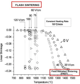
Although, FS is not observed and Joule heating is substantially negligible the field application enhances the densification. In Figure 21 the two sintering regime are highlighted. If the field exceed 60 V/cm FS is observed with an almost instantaneous densification. In the case of lower field strength FAST takes place[6]. In FAST regime the densification can be anticipated of ~200°C with respect to conventional
Figure 21: FS and FAST regime in YSZ upon constant heating rate experiments (10°C/min). Modified from [6].
1.6.7 Flash reactions
2 Aim of the work
Up to date, the research on flash sintering has been mainly focused on ionic and electronic conductors and on semiconductors. Only one work has investigated the flash sintering behavior of insulating materials like high purity and MgO-doped alumina [39]. Nevertheless, many technical ceramics (i.e. refractories, high temperature materials…) are resistive. This represents an evident lack in the scientific knowledge of this process.
Another point that has not been deeply investigated yet is the flash sintering behavior of materials constituted by the simultaneous presence of a crystalline and glassy phase. Such materials represents the larger part of ceramics market: many advanced ceramics are sintered with the addition of a glass for promoting liquid phase sintering, while all the traditional ceramics are characterized by a vitrification process upon sintering. Additionally, the recent findings on Electric Field-Induced Softening has increased the scientific interest on this topic.
In the present work, we tried to fill part of these two gaps. At first, we studied the flash sintering behavior of a resistive technical ceramic like alumina, which is widely used in many applications as pointed out by the huge world production exceeding 50 million tons per year[127]. Flash sintering experiments were carried out on commercially pure alumina CT3000SG (99.8% pure), manufactured by ALCOA. Then, we extended our analysis to a common mixed system containing both crystalline (alumina) and glassy (magnesia silicate glass) phase. The experimental and analytical activity was carried out with the aim to clarify and understand some of the several mechanisms behind flash sintering.
3 Experimental procedures
3.1 Materials and samples preparation
In this work, low soda reactive α-alumina from ALMATIS - CT3000SG, 99.8% pure, was used. The nominal composition of the powder is reported in Table III. The powder is characterized by d50 = 600 nm and a specific surface area of 7.8 m2/g. Such alumina powder is commercially available and widely used because of its good sinterability. At the same time it seems suitable for flash sintering experiments because of the presence of several impurities, which may enhance electrical conductivity. Higher purity alumina has already been subjected to FS experiments pointing out that they are too resistive for triggering the flash event[39]. A more detailed discussion of the material composition and its effect on flash sintering, compared with previous experimental results [39], is reported in “4.1.1 Densification behavior and microstructural evolution”.
Table III: Nominal composition of the alumina powder used in in this work.
[wt%]
Al2O3 99.8
Na2O 0.03
Fe2O3 0.015
SiO2 0.015
MgO 0.040
CaO 0.015
milled in isopropyl alcohol using alumina spheres for 3 h. The suspension was then dried and calcined in a muffle furnace (Nabertherm P180) under static air atmosphere using heating rate of 10°C/min up to 750°C and dwell time of 30 min. The nominal composition of the obtained material was: 90 wt% Al2O3, 8wt% SiO2 and 2 wt% MgO. Hence, the glass load in the material was 10 wt% and the composition was 80 wt% silica and 20 wt% magnesia.
For comparison, following the same procedures, also high purity silica glass was obtained and added to alumina. In this case the nominal composition of the material was 90 wt% Al2O3, 10 wt% SiO2.
The three different powder (pure alumina, magnesia-silicate and pure silica-containing alumina) were then mixed with some water as a binder (6 – 7 wt%). The specimens were shaped by uniaxial pressing in dog bone shape at 120 MPa, using the geometry reported in Figure 22. The sample thickness varies from 2.8 to 3.3 mm. The chosen geometry was substantially the same of that used in many flash sintering experiments like those reported in Figure 15; unless the sample thickness used in the present work was slightly higher.
Figure 22: Specimen geometry used for flash sintering experiments (quote in mm).
The platinum electrodes were connected to a DC power supply (Glassman EW series 5 kV–120 mA) and to a digital multimeter (Keithley 2100). In this way it has been possible to record voltage and current at 1 Hz.
3.2 Experimental set-up n. 1
Figure 23: Experimental set-up for constant heating rate experiments.
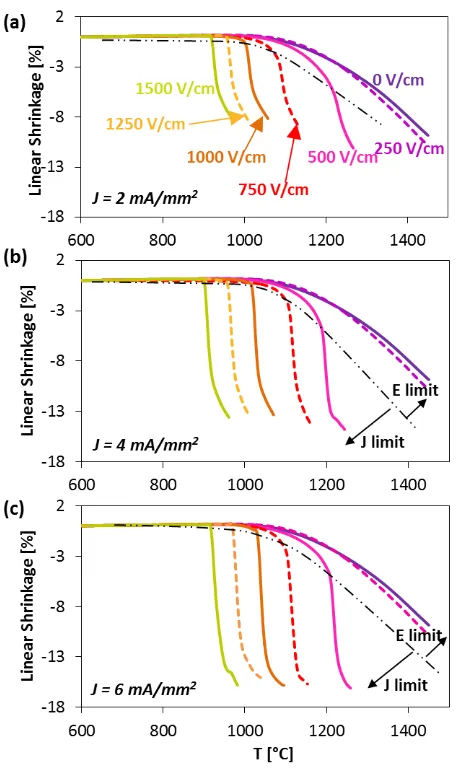
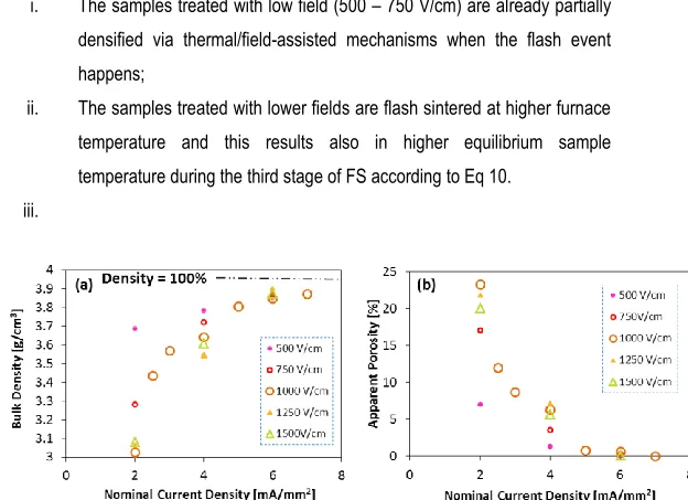
The system starts to work in voltage control in the range 250 – 1500 V/cm. After the flash event the system switches in current control and the current was let to flow in the specimen for 2 min. After that the power supply and the furnace were shut down. Currents in the range 0.6 – 7 mA/mm2 were used for the experiments.
The electrical parameters (current and tension) were recorded using a digital multimeter (Keithley 2100). Current density, field and specific power dissipation were calculated taking in account of the actual sample size (assuming isotropic shrinkage). If these values are calculated with respect the green body dimension they are defined in the text as “nominal”.
3.3 Experimental set-up n. 2
After pre sintering, the specimens were connected by two platinum wires to a DC power supply (Glassman EW series 5 kV–120 mA) and to a digital multimeter (Keithley 2100). The specimen was then introduced in a pre-heated tubular furnace (Nabertherm P330) at 1200°C and subjected to flash sintering using different combination of E and J.
An optical fiber was placed on the bottom of the furnace for recording the optical emission spectra during the flash event. For this purpose two different spectrometer were used: NIR 512 and USB4000 for the NIR and UV/VIS region, respectively. The data in the UV/VIS were recorded using an integration time of 3.8 ms, whereas in the NIR the integration time was fixed in 10 ms. The optical response of the system was properly corrected using a calibration lamp (Avantes, HD2000).
Using this experimental set-up the electrical conductivity of alumina pre-sintered at different temperature was measured at 1200°C using field in the range 500-1500 V/cm.
![Figure 8: Sample length effect on incubation time for FS in Al2O3/YSZ composites (a)[56]](https://thumb-us.123doks.com/thumbv2/123dok_us/523092.2052075/30.420.72.357.42.258/figure-sample-length-effect-incubation-time-ysz-composites.webp)
![Figure 9: Relation between onset temperature for FS and applied field for 8YSZ in AC and DC treatments.[57]](https://thumb-us.123doks.com/thumbv2/123dok_us/523092.2052075/31.420.78.349.45.264/figure-relation-onset-temperature-applied-field-ysz-treatments.webp)
![Figure 20: Textured SiC obtained by flash spark plasma sintering. Taken from [110].](https://thumb-us.123doks.com/thumbv2/123dok_us/523092.2052075/55.420.80.333.42.255/figure-textured-obtained-flash-spark-plasma-sintering-taken.webp)