Adiabatic circuits: converter for static CMOS signals
J. Fischer, E. Amirante, A. Bargagli-Stoffi, and D. Schmitt-Landsiedel
Institute for Technical Electronics, Technical University Munich, Theresienstrasse 90, D-80290 Munich, Germany
Abstract. Ultra low power applications can take great ad-vantages from adiabatic circuitry. In this technique a mul-tiphase system is used which consists ideally of trapezoidal voltage signals. The input signals to be processed will often come from a function block realized in static CMOS. The static rectangular signals must be converted for the oscillat-ing multiphase system of the adiabatic circuitry. This work shows how to convert the input signals to the proposed pulse form which is synchronized to the appropriate supply volt-age.
By means of adder structures designed for a 0.13µm technology in a 4-phase system there will be demonstrated, which additional circuits are necessary for the conversion. It must be taken into account whether the data arrive in par-allel or serial form. Parpar-allel data are all in one phase and therefore it is advantageous to use an adder structure with a proper input stage, e.g. a Carry Lookahead Adder (CLA). With a serial input stage it is possible to read and to process four signals during one cycle due to the adiabatic 4-phase system. Therefore input signals with a frequency four times higher than the adiabatic clock frequency can be used. This reduces the disadvantage of the slow clock period typical for adiabatic circuits. By means of an 8 bit Ripple Carry Adder (8 bit RCA) the serial reading will be introduced. If the word width is larger than 4 bits the word can be divided in 4 bit words which are processed in parallel. This is the most ef-ficient way to minimize the number of input lines and pads. At the same time a high throughput is achieved.
1 Introduction
Adiabatic circuitry can save energy in the frequency domain up to about 100 MHz which is interesting for digital signal processing. The family considered in this work is the Pos-itive Feedback Adiabatic Logic (PFAL) (Vetuli et al., 1996; Blotti et al., 2000) because it has very low energy dissipation
Correspondence to: J. Fischer (juergen.fischer@ei.tum.de)
and shows the best performance at high frequencies. The needed signal waveforms are equivalent to the signals for Ef-ficient Charge Recovery Logic (ECRL) and 2N-2N2P (Moon et al., 1996; Kramer et al., 1995). These families use sym-metrical trapezoidal supply voltages and dual rail encoded input/output signals. A comparison of ECRL, 2N-2N2P and PFAL was performed in Amirante et al. (2001) regarding to the frequency dependent energy dissipation and the robust-ness against parameter variations. The energy dissipation can amount 13% or less than that of static CMOS which has the fundamental limit of12CVDD2 .
The goal of this paper is to present the integration of adia-batic function blocks in a standard CMOS environment. The important circuits for this matter are the converters. They consist not only of a stage which converts the signal into the right pulse shape and phase but also of a synchronizing cir-cuit. The design of the entire conversion stage is compara-ble to the one for static CMOS buffer stages. For synchro-nizing the incoming signal from the static CMOS block to the supply clock of the adiabatic circuits the 4-phase system will provide the timing information. Thus the benefits of this system will be explained first before the synchronized con-verter is presented. Adder structures vary in the way the data can be applied to their input. The Carry Lookahead Adder (CLA) which is the best choice for internal data (Amirante et al., 2002) needs parallel input data. That means the input data are driven by the same phase. The Ripple Carry Adder (RCA) with its cascaded full adders can also handle serial data. This is useful for off-chip data sources. The number of pads is often limited so that a serial input is necessary. By the right arrangement of the converters, the RCA can be used for the serial input without any additional buffer stages.
2 4-phase system
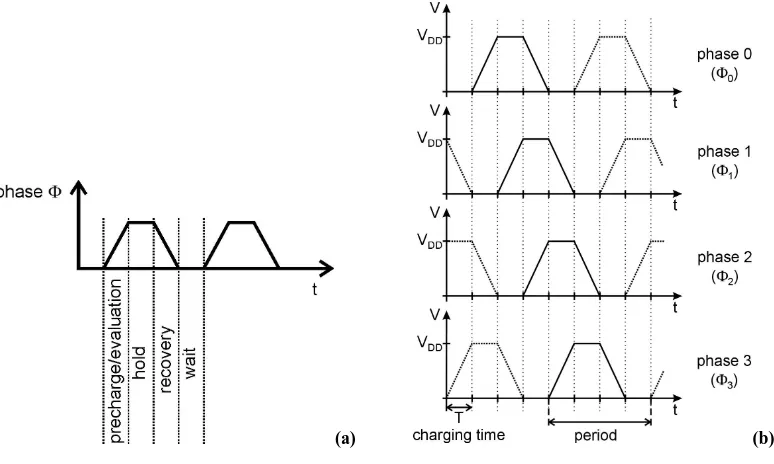
(a) (b)
Fig. 1. 4-phases system, (a) one phase with the four states: evaluation, hold, recovery and wait, (b) 4 phases and their 90 degree shift.
energy dissipation is low even at high frequencies. Because of the dual rail encoding the oscillator sees a constant load and the design of high efficiency oscillators has been sim-plified. A presentation of an oscillator design is given in Bargagli-Stoffi et al. (2002). The ideal waveform for the sup-ply voltage is shown in Fig. 1a. It can be divided in four states of equal length. The precharge/evaluation state is character-ized by the increasing voltage ramp, which allows to load the capacitance efficiently regarding to energy dissipation. Dur-ing the hold state the output value is valid and can be evalu-ated by the next stage. By decreasing the voltage a recovery of energy is achieved. During the wait state the supply volt-age is zero and no leakvolt-age current flows. As mentioned be-fore the evaluation of one stage and the holding of the former stage have to take place at the same time so that two subse-quent phases are shifted by 90 degrees (Fig. 1b). Altogether there are four phases, and during one period four functions can be executed. Thus the effective throughput rate can be up to four times higher than the adiabatic clock frequency. In or-der to reach the minimum energy dissipation the value of 90 degree shift should be achieved exactly by proper oscillator design . Because of this accurate relation between the phases the synchronization signal can be extracted from them.
3 Converter
3.1 Basic input converter without synchronization
The prerequisite of the presented converter is the presence of the supply clocks with their accurate trapezoidal wave-form. These signals will also act as supply for the intrinsic converter (Fig. 2a). Thus the pulse shaping will be provided by the oscillator and the static signals only need to control
switches. If the output node follows the supply clock it will be at a HIGH level in adiabatic circuitry. Otherwise if the output stays at ground the signal is at the LOW level. In or-der to generate an adiabatic high level a transmission gate is the best choice as pull-up tree. The provided trapezoidal supply clock can pass the transmission gate without distur-bances, such as voltage steps due to the threshold voltage. The dimensioning of the transmission gate should follow that for static CMOS. The equivalent resistance must fit the re-quirements. In adiabatic circuitry the delay of the stages is not important but the energy dissipation which is strongly dependent on the resistance. The dimensioning of the trans-mission gate or the minimization of the equivalent resistance is a tradeoff between area consumption and energy dissipa-tion. In order to avoid a deformation of the adiabatic sig-nal, the static CMOS input signal of the converter must not be switched during the whole precharge, hold and recov-ery states. Thus the static signal switches only during the wait state, when the supply clock is at ground. To generate an adiabatic low level, the output has just to be clamped at ground. Therefore a n-channel transistor is sufficient as pull-down tree. Because the resistance of the n-channel transistor does not influence the energy dissipation its dimension can be chosen minimal.
3.2 Input converter with synchronization
In order to produce a dual rail encoded trapezoidal signal with the phase81two basic converters are needed (Fig. 2b). They are driven by a static CMOS D-register generating the input and the inverted input signal. To avoid metastability cascaded registers are used. A comparator which compares the preceding supply voltage phase80with half ofVDD
Fig. 2. (a) Basic converter; a rectangular signal is converted into an inverted trapezoidal one by a trapezoidal adiabatic supply voltage, (b) converter with synchronization circuit to generate dual rail encoded trapezoidal signals.
(a) (b)
Fig. 3. (a) Timing diagram of a converter stage, the supply voltage80is compared toVDD/2 generating the clock for the registers, the
register switches only in the waiting state of the supply voltage81, (b) taking advantage from the 4-phase system, the serial reading can be
done with four times the frequency of the trapezoidal clock.
As mentioned above the static input signal must switch only during the wait state of the supply voltage. The syn-chronization is explained in Fig. 3a for an adiabatic signal having the phase81. To have a robust synchronization the switching point should be in the middle of the wait state of 81that is simultaneous to the precharge state of the preced-ing phase (80) . The clock signal can easily be generated by comparing80withVDD/2. The simplest comparator for this
use is a static CMOS buffer. Of course the delay of the buffer and the register must not exceed half of the wait state which is one eighth of the adiabatic clock period. In most cases, this is fulfilled even with minimal dimensioned gates because of the rather long adiabatic clock period. Because of the exact relation between two phases mentioned in Sect. 2, the whole margin amounts one eighth of the period. To improve the delay an inverter can be used instead of a buffer. But in this caseVDD/2 must be compared with the next stage82which is in the recovery stage or a negative edge-triggered register must be used.
The comparators generate clock signals with the same 90 degree shift as the oscillator (see Fig. 3b). An input bitstream applied to all these converters will be sampled by each stage at another specified time. Thus a 4bit word can be transmitted per adiabatic period and the input rate is increased by a factor of four. Of course every output bit of such a 4bit converter has its own phase. If all output data should have the same phase additional buffer stages must be inserted.
3.3 Output converter
Fig. 4. Schematic of an 32bit-carry lookahead adder (32-bit CLA) with input and output converters. The terms of the sum A and B are converted by the first stage into 64 dual rail encoded adiabatic signals. The output conversion is performed by D-registers.
4 Adder structures
Many adder structures for static CMOS are demonstrated in Weste, Eshraghian (1992). Most of them can be adapted for adiabatic circuitry. Adders realized in adiabatic circuitry are pipelined structures. Therefore it is possible to apply new data to the input every cycle although it can take longer than one period to get the result. Adiabatic adder structures differ mainly from static CMOS in how long it takes to perform the whole addition.
4.1 Carry Lookahead Adder (CLA)
The carry lookahead adder consists of three parts (Fig. 4). The first stage generates the ’propagate’ and the ’generate’ signals. These signals are used in the second part to cal-culate the carry information. In the last stage the sum is built. The important part is the carry generation because by a proper implementation the number of phases can be reduced. The algorithm shows its whole potential if the word width is larger than 8 bit especially for adiabatic circuits. In or-der to support the adiabatic system design the output signals should all have the same phase which can be evaluated by the subsequent input stage. Then you do not have to care about the phases and automatic placement will work like in static CMOS. Hence one function block should consist of a multiple of four stages. If the word width is smaller than 32 bit additional buffer stages must be integrated to have the proposed output phase. One addition of 32bit will take two adiabatic periods but in every period new data can be fed to the input stage because of the intrinsic pipelined structure of adiabatic circuitry. For internal addition of wide data words the CLA is the preferred choice.
In Fig. 4 also the integration of a CLA into a static CMOS environment is shown. The synchronized converters must provide the parallel input data with the phase83so that the first stage with the phase80can evaluate it. Therefore 32 converters per term of the sum are synchronized by the phase 82. The output signals have the phase83. If they should be converted to static signals positive edge triggered D-registers
are used whose clock signal is generated by a comparison of the subsequent phase80andVDD/2.
4.2 Ripple Carry Adder (RCA)
A ripple carry adder is built by cascading several full adders. Therefore the time needed for the addition is proportional to the word width, e.g. an 8 bit RCA consists of eight full adders and the addition will take two adiabatic periods. Like in the CLA in every period new data can be fed into the pipeline. So the response time between applying data to the input and receiving the sum at the output is a major drawback of adia-batic RCAs if the word width gets large.
The RCA is especially suitable with serial inputs. The 4bit word converters of Sect. 3.2 transform the data in 4 signals which can directly drive the input stage of the RCA without any additional buffer stages. The minimal number of pads is achieved if the data consists of one bitstream for each term of the sum (Fig. 5a). This bitstream is divided by an internal demultiplexer into 4 bit words which are converted by the 4 bit word converters. However, as long as the most significant bits (MSBs) are applied to the adder input no valid data are present at the input of the least significant bits (LSBs) and vice versa. Therefore, time which could have been used for processing is wasted and the throughput decreases with larger word width. In order to maximize the throughput the data must be partitionated into parallel bitstreams with forefield multiplexing. This results in two pads in the case of an 8bit RCA (Fig. 5b). First the 4 LSBs are applied to the first pad. During the next period the 4 MSBs appear at the second pad. Because of the pipelined structure of adiabatic circuitry the LSBs of the next term of the sum can drive the first pad. Of course this principle can be expanded for larger word width.
Fig. 5. Addition of 4 bit words with a 8 bit RCA, (a) minimizing number of pads by using internal demultiplexer and 4 bit word converter, (b) maximal throughput without internal demultiplexing.
minimized or avoided. The testchip has not been measured yet but simulations performed with extracted parasitics from the layout show that the presented converter principles will work at frequencies beyond 100 MHz. The interface between the static CMOS and the adiabatic circuits can be designed fast enough, and therefore robust enough, to meet the re-quirements in the frequency domain in which adiabatic cir-cuitry saves a large amount of energy.
5 Conclusion
In this work principles are presented which allow to inte-grate adiabatic function blocks into static CMOS circuits. A synchronized converter is used to generate the dual rail encoded trapezoidal signals which are necessary for the con-sidered adiabatic families PFAL, ECRL and 2N-2N2P. Inside the converter a comparator is used to extract the clock signal for synchronizing the input signal. This clock signal can be used for every timing issue between the two circuitries. The robustness of this signal is an issue of oscillator and com-parator design. The oscillator must provide the circuit with four phases which have an exact difference of 90 degrees, otherwise the energy dissipation increases. The compara-tor’s delay is well known and can be adjusted regarding to the timing conditions. By combining the serial input data to 4bit words, the input rate can be increased by a factor of four. This principle can be used to minimize pads at the input. It is also worth noticing that the throughput rate of adiabatic cir-cuits is up to four times higher than the adiabatic frequency because of the 4-phase system.
The embedding of adiabatic circuits into a static CMOS environment was a major concern for the use in real appli-cation. This issue has now been solved. Adiabatic circuits allow to save energy in a frequency range typical for digital signal processing applications. Therefore adiabatic circuitry can be a suitable ultra low power strategy for digital signal processing in the frequency domain up to hundreds of MHz.
Acknowledgements. The authors would like to thank Infineon
Tech-nologies AG, in particular Dr. C. Heer, Dr. J. Berthold und Dr. R. Nadal for their help with the design and for useful discussions and advices.
This work is funded by the German Research Foundation (DFG) under the grant SCHM 1478/1-2.
References
Amirante, E., Bargagli-Stoffi, A., Fischer, J., Iannaccone, G., and Schmitt-Landsiedel, D.: Variations of the Power Dissipation in Adiabatic Logic Gates, Proceedings of the 11th International Workshop on Power And Timing Modeling, Optimization and Simulation, PATMOS’01, Yverdon-les-Bains, Switzerland, pp. 9.1.1–9.1.10, September 2001.
Amirante, E., Bargagli-Stoffi, A., Fischer, J., Iannaccone, G., and Schmitt-Landsiedel, D.: Adiabatic 4-bit Adders: Comparison of Perfomance and Robustness against Technology Parameter Variations, 45th Midwest Symposium on Circuits and Systems, MWSCAS’02, Tulsa Oklahoma, USA, August 2002.
Bargagli-Stoffi, A., Amirante, E., Fischer, J., Iannaccone, G., and Schmitt-Landsiedel, D.: Resonant 90 Degree Shifter Generator for 4-Phase trapezoidal adiabatic logic, U.R.S.I. Kleinheubacher Tagung 2002, Miltenberg, Germany, 30 Sep–02 Oct 2002. Blotti, A., Di Pascoli, S., and Saletti, R.: Simple model for
positive-feedback adiabatic logic power consumption estimation, Elec-tronics Letters, 36, 2, 116–118, 2000.
Kramer, A., Denker, J. S., Flower, B., and Moroney, J.: 2nd order adiabatic computation with 2N-2P and 2N-2N2P logic circuits. Proceedings of the International Symposium on Low Power De-sign, 191–196, 1995.
Moon, Y. and Jeong, D.: An Efficient Charge Recovery Logic Cir-cuit. IEEE Journal of Solid-State Circuits, 31, 4, 514–522, 1996. Vetuli, A., Pascoli, S. D., and Reyneri, L. M.: Positive feedback in
adiabatic logic, Electronics Letters, 32, 20, 1867–1869, 1996. Weste, N. H. E. and Eshraghian, K.: Principles of CMOS VLSI