Adv. Radio Sci., 5, 297–304, 2007 www.adv-radio-sci.net/5/297/2007/ © Author(s) 2007. This work is licensed under a Creative Commons License.
Advances in
Radio Science
Design of UWB pulse radio transceiver using statistical correlation
technique in frequency domain
M. Anis and R. Tielert
Institute for Microelectronics, Technical University of Kaiserslautern, Germany
Abstract. In this paper, we propose a new technique to
ex-tract low power UWB pulse radio signals, near to noise level, using statistical correlation technique in frequency domain. The receiver consists of many narrow bandpass filters which extract energy either from transmitted UWB signal, interfer-ing channels or noise. Transmitted UWB data can be elim-inated by statistical correlation of multiple bandpass filter outputs. Super-regenerative oscillators, tuned within UWB spectrum, are designed as bandpass filters. Summers and comparators perform statistical correlation.
1 Introduction
In the last few years, UWB pulse radio has become attractive for low power and low cost short range applications, espe-cially in wireless body area networks. WBAN requires in-novative solutions to meet the energy consumption budget of the autonomous sensor nodes. Today’s low power radio sys-tems like Bluetooth and Zigbee do not meet these require-ments, but the pulse based UWB reaches the target. It is an effective technique to deliver short range communication, us-ing very short pulses and wide spectrum, enables coexistence with other narrow band radio systems. To mitigate the effects of interference to UWB from noise and other radio systems, we propose statistical correlation technique in frequency do-main.
This paper describes the design of the first UWB CMOS transceiver, having ability to extract the UWB signal from the noise level. Our proposed architecture is based on simple on-off keying for low and medium data rate UWB system. The transmitter generates a pseudo random pattern of UWB impulses in a sub nanosecond time scale. The receiver con-sists of many narrow band pass super regenerative oscillators Correspondence to: M. Anis
Filter @ f1
Filter @ f2
Filter @ f3
SUMMER Comparator for 1 s Ref. Volt
Vsum(t)
UWB Transmitter
1 0 1 UWB Data
+
Noise
+
Interference with in UWB spectrum
Fig. 1. OOK Low Data Rate UWB RF Front End Block Diagram
1
2σ
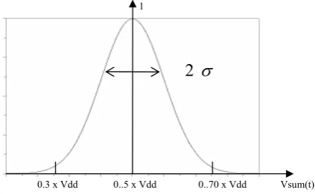
0.3 x Vdd 0..5 x Vdd 0..70 x Vdd Vsum(t)
Fig 2. The Probability distribution function of Vsum(t), in the absence of UWB data
Vsum(t) High S/N ratio High S/N ratio Low S/N ratio
1 PDF
0 0.5 x Vdd Vdd
Fig.3 Probability distribution function of Vsum(t), in the presence of UWB data
1s 0s
Fig. 1. OOK Low Data Rate UWB RF Front End Block Diagram.
Filter @ f1
Filter @ f2
Filter @ f3
SUMMER Comparator for 1 s Ref. Volt
Vsum(t)
UWB Transmitter
1 0 1 UWB Data
+
Noise
+
Interference with in UWB spectrum
Fig. 1. OOK Low Data Rate UWB RF Front End Block Diagram
1
2
σ
0.3 x Vdd 0..5 x Vdd 0..70 x Vdd Vsum(t)
Fig 2. The Probability distribution function of Vsum(t), in the absence of UWB data
Vsum(t) High S/N ratio
High S/N ratio Low S/N ratio
1 PDF
0 0.5 x Vdd Vdd
Fig.3 Probability distribution function of Vsum(t), in the presence of UWB data
1s 0s
Fig. 2. The Probability distribution function of Vsum(t), in the ab-sence of UWB data.
(SRO), tuned within UWB spectrum, acting as narrow band-pass filters. These SROs can be triggered either by the noise, interference or either by transmitted UWB data. Noise and interferences due to other radio channels are uncorrelated in all filter (SRO) outputs. UWB data are extracted after the sta-tistical correlation of multiple bandpass filter outputs. Statis-tical correlation is performed by summer and comparator.
298 M. Anis et al.: Design of UWB pulse radio transceiver using statistical correlation technique in frequency domain Filter @ f1
Filter @ f2
Filter @ f3
SUMMER Comparator for 1 s Ref. Volt
Vsum(t) UWB
Transmitter
1 0 1 UWB Data +
Noise +
Interference with in UWB spectrum
Fig. 1. OOK Low Data Rate UWB RF Front End Block Diagram
1
2
σ
0.3 x Vdd 0..5 x Vdd 0..70 x Vdd Vsum(t)
Fig 2. The Probability distribution function of Vsum(t), in the absence of UWB data
Vsum(t) High S/N ratio
High S/N ratio Low S/N ratio
1 PDF
0 0.5 x Vdd Vdd Fig.3 Probability distribution function of Vsum(t),
in the presence of UWB data
1s 0s
Fig. 3. Probability distribution function of Vsum(t), in the presence of UWB data.
Glitch generator State Machine 1 State Machine 2 Delay Stages UWB Pulse Shaper Data_In Astable
Multivibrator
Fig. 4 Block diagram of UWB transmitter
1
0 5 G 10G
Fig. 5a Normalize power density spectrum of periodic UWB impulses
1
0 5 G 10G
Fig. 5b Normalize power density spectrum of PN sequence of UWB impulses
Fig. 6 Astable multivibrator with additional switches and capacitors
Fig. 4. Block diagram of UWB transmitter.
2 System overveiw
The proposed architecture based on statistical correlation in frequency domain is designed to extract the UWB signals which are embedded into noise and interfering channels. The UWB transmitter generates the pseudo random pattern of UWB impulses during on time of on-off modulation keying. The maximum energy level of UWB signal is near to noise level.
Figure 1 shows the UWB receiver which consists of mul-tiple narrow band pass filters, tuned within the UWB spec-trum. These filter banks will extract energy either from UWB transmitted data, noise or interfering channels. Outputs of fil-ter banks due to noise are uncorrelated in each channel. Nar-row band interfering channels like WLAN can disturb one or two filter channels. When the transmitted UWB data with embedded noise and interfering channels are present at an-tenna, a majority of the filter bank outputs will be correlated due to UWB data. Filter banks of frequency range 6 GHz– 8.5 GHz are designed by super-regenerative oscillators. The SRO was invented in 1922 by Armstong, well suited for short range low power applications. The SRO is turned on and off by a quench signal. The start up time of the SRO depends on the matching of tuned LC tank frequency and signal
fre-Glitch generator State Machine 1 State Machine 2 Delay Stages UWB Pulse Shaper Data_In Astable
Multivibrator
Fig. 4 Block diagram of UWB transmitter
1
0
5 G 10G
Fig. 5a Normalize power density spectrum of periodic UWB impulses
1
0
5 G 10G
Fig. 5b Normalize power density spectrum of PN sequence of UWB impulses
Fig. 6 Astable multivibrator with additional switches and capacitors
Fig. 5a. Normalize power density spectrum of periodic UWB im-pulses. Glitch generator State Machine 1 State Machine 2 Delay Stages UWB Pulse Shaper Data_In Astable
Multivibrator
Fig. 4 Block diagram of UWB transmitter
1
0
5 G 10G
Fig. 5a Normalize power density spectrum of periodic UWB impulses
1
0
5 G 10G
Fig. 5b Normalize power density spectrum of PN sequence of UWB impulses
Fig. 6 Astable multivibrator with additional switches and capacitors
Fig. 5b. Normalize power density spectrum of PN sequence of UWB impulses
quency of received input. Twelve SROs, each using an LC filter tank have been integrated in our test structure. The out-put of every SRO is connected with envelop detectors, in or-der to get the output of each channel in digital form.
The most critical point is the biasing of SROs. The bias point of all SROs is adjusted so that average output voltage of each channel should be half of the supply voltage. In the absence of RF UWB signals, regulator increases the bias cur-rent of all SROs to make them sensitive to noise level, which means that every SRO has 50% probability to be triggered due to noise and the summation of all filter (SROs + envelop det.) outputs Vsum(t) has a Gaussian distribution, as shown in Fig. 2. When the modulated UWB data having energy level near to noise is radiated by transmitter, the probability to detect 1s increases in all channels. The regulator starts to decrease the bias current of all SROs, to maintain the average output voltage of each channel at the half of supply voltage. The UWB data can be extracted by comparing the summer output to the half of supply voltage.
Vsum(t ) >0.5×V dd⇒1
Vsum(t ) <0.5×V dd⇒0
Figure 3 shows the probability distribution function of Vsum(t) in the presence of UWB data. The distribution func-tions for detecting 1 s and 0 s move towards the 50% of sup-ply voltage for signals having small S/N ratios and move
M. Anis et al.: Design of UWB pulse radio transceiver using statistical correlation technique in frequency domain 299
Glitch generator
State Machine 1
State Machine 2
Delay Stages
UWB Pulse Shaper Data_In Astable
Multivibrator
Fig. 4 Block diagram of UWB transmitter
1
0
5 G 10G
Fig. 5a Normalize power density spectrum of periodic UWB impulses
1
0
5 G 10G
Fig. 5b Normalize power density spectrum of PN sequence of UWB impulses
Fig. 6 Astable multivibrator with additional switches and capacitors
Fig. 6. Astable multivibrator with additional switches and capaci-tors.
0
66n 67n 68n 69n 70n Æ t ns
1.5 V
Fig. 7a Pseudo random pattern at the output of astable multivibrator
66n 67n 68n 69n 70n Æ t ns 0
1.5 V
Fig. 7b Pseudo random pattern at the output of glitch generator
Fig. 8 Circuit diagram of basic glitch generator
Glitch generator output
Fig. 9 Delay Stages & UWB Pulse Shaper
Fig. 7a.Pseudo random pattern at the output of astable multivibrator.
away from the 50% of supply voltage for signals having high S/N ratios as shown in Fig. 3.
3 UWB transmitter
A fully integrated pulse generator for impulse based UWB system, covers the spectrum of 6–8.5 GHz, and was designed on 0.18µm CMOS technology. On/off modulation scheme is used. The basic structure consists of four parts, astable mul-tivibrator with state machines, glitch generator, delay stages and UWB pulse shaper, shown in Fig. 4. Astable multivi-brator (Baker et al., 1997) with state machines is used to generate the pseudo random (PN) pattern of UWB impulses. The periodic repetition of impulses generates the large spikes over the UWB spectrum. The PN sequence is used to flatten the UWB spectrum (Maggio et al., 2001). The simulation for power spectrum of periodic and PN sequence of impulses are shown in Figs. 5a, b.
The basic structure of astable multivibrator can generate periodic signals of pulse width t∼0.65 RC. Three switches (SData I n, S1, S2)and two capacitors (C2, C3) are added to
the astable multivibrator as shown in Fig. 6. Switch SDat a I n,
connected to input digital data, will turn the multivibrator on and off. On-off keying modulation is used to transmit UWB pattern. When the switch is closed, multivibrator will be off and UWB pulse shaper will not transmit the UWB impulse. When the switch is open, multivibrator generates the pattern
0
66n 67n 68n 69n 70n Æ t ns
1.5 V
Fig. 7a Pseudo random pattern at the output of astable multivibrator
66n 67n 68n 69n 70n Æ t ns
0
1.5 V
Fig. 7b Pseudo random pattern at the output of glitch generator
Fig. 8 Circuit diagram of basic glitch generator
Glitch generator output
Fig. 9 Delay Stages & UWB Pulse Shaper
Fig. 7b. Pseudo random pattern at the output of glitch generator.
0
66n 67n 68n 69n 70n Æ t ns
1.5 V
Fig. 7a Pseudo random pattern at the output of astable multivibrator
66n 67n 68n 69n 70n Æ t ns
0 1.5 V
Fig. 7b Pseudo random pattern at the output of glitch generator
Fig. 8 Circuit diagram of basic glitch generator
Glitch generator output
Fig. 9 Delay Stages & UWB Pulse Shaper
Fig. 8. Circuit diagram of basic glitch generator.
of pulse width t∼0.7 RCeq, where Ceqis the sum of
capaci-tances selected by state machines and parasitics of connected transistors. Initially the multivibrator generates a periodic rectangular pattern due to capacitor C2. The output of
multi-vibrator is connected to the clock signal of two different state machines. These state machines generate the defined pattern used to select and deselect the capacitors by switches S1 and S2. Due to the changing of Ceq pulse width of the
multivi-brator changes, resulting in different clock rates of the cycles which generates the pseudo random pattern at the output, as shown in Fig. 7a.
The UWB pulses require sharp rising and falling transi-tions. Due to the different rise and fall transition times of the multivibrator, two different pulse shapes and spectrum will be generated. In order to avoid this problem, very small glitches are generated on each rising edge of pattern. Fig-ure 7b shows the simulation results of the PN sequence at the output of the glitch generator. Figure 8 shows the cir-cuit diagram of basic glitch generator. The delay stages are designed by a chain of basic CMOS inverters (Jeong et al., 2004). Delay stages generate three delayed small glitches. The delays are adjusted by the W/L ratios of inverters. These delays in between the glitches are smaller than the widths of glitches. These three glitch stages are connected to a UWB pulse shaper, consisting of three LC resonators tuned within 6–8.5 GHz range. Chirped UWB pulses with flat spectrum of 6–8.5 GHz are achieved after mixing the outputs. Figure 9 shows the delay stages and UWB pulse shaper. Figure 10 shows the simulated pattern of UWB pulses at the load of 50.
300 M. Anis et al.: Design of UWB pulse radio transceiver using statistical correlation technique in frequency domain
Please correct the following points
1) On top right side of every paper you wrote
M.
Anis and R. Tieler:
Correct one is
M.Anis and R. Tielert
2) On page 2 , comments on of Fig 5a is wrong, you wrote
Fig. 5a Normalize power density spectrum of PN sequence of UWB
impulses
Correct one is
Fig. 5a Normalize power density spectrum of periodic UWB
impulses
3) on page 2, you wrote
Vsum(t) > 0.5 × V dd => 0
Vsum(t) < 0.5 × V dd => 1
Correct is
Vsum(t) > 0.5 × V dd => 1
Vsum(t) < 0.5 × V dd => 0
4) on page 4, line in middel of fig. 9. is wrong
Correct fig. is
Fig. 9. Delay stages and UWB Pulse Shaper.
5) on page 7, you wrote
6
UWB receiver
7
Conclusion
Correct on is
5.2
UWB receiver
6 Conclusion
Fig. 9. Delay Stages and UWB Pulse Shaper.
0 50n 100n 150n Æ time(s) 110n 120n 130n Æ time(s) 119n 120n 121n Æ time(s)
100m (V) 0 -25m 100m (V) 0 -25m 100m (V) 0 -25m
Fig.10 The simulated pattern of UWB pulses at the load of 50Ω
Fig. 10. The simulated pattern of UWB pulses at the load of 50.
4 UWB receiver
A fully integrated UWB pulse receiver covering the spectrum from 6–8.5 GHz has been implemented in 0.18µm CMOS technology. Figure 1 shows the block diagram of the receiver. The simple low power system consists of isolation amplifier, super regenerative oscillators, envelop detectors, data syn-chronizers and regulated current control units, as shown in Fig. 11. The RF UWB signal is first fed to the isolation am-plifier (IA). This common gate amam-plifier provides isolation of
Current Control Uniit SRO @ 6.1 GHz Envelop detector Data Sync. Current Control Uniit SRO @
6.3 GHz Envelop detector Sync. Data
Current Control Uniit
SRO @
6.5 GHz Envelop detector SyncData . IA Quench Signal Clock distribution unit IA IA S U M M E R
Fig.11 Block diagram of multiple narrow band filter banks
IA A
Selective network Quench Signal
Env. Det.
Fig 12. Block diagram of super-regenerative oscillator
Fig. 11. Block diagram of multiple narrow band filter banks.
Current Control Uniit SRO @ 6.1 GHz Envelop detector Data Sync. Current Control Uniit SRO @ 6.3 GHz Envelop detector Data Sync. Current Control Uniit SRO @ 6.5 GHz Envelop detector Data Sync. IA Quench Signal Clock distribution unit IA IA S U M M E R
Fig.11 Block diagram of multiple narrow band filter banks
IA
A
Selective network Quench Signal
Env. Det.
Fig 12. Block diagram of super-regenerative oscillator
Fig. 12. Block diagram of super-regenerative oscillator.
antenna and SROs. The signal then goes to SROs controlled by a feedback network as shown in Fig. 12. These oscillators are tuned within the range of the UWB signal spectrum 6– 8.5 GHz. All oscillators are turned on and off by one quench generator. The start up time of the individual oscillators de-pends on the received input power and its frequency. The oscillator will start early, when the received signal is near to the center frequency of the oscillator. Without any RF signal, the start up time of oscillators depends on the feedback gain and thermal noise (Moncunill et al., 2005). Figure 13 shows the simulation results of four different SROs with on –off modulation for UWB. Selectivity and sensitivity, frequency and shape of the quench signal, minimum and maximum lev-els of bias currents of oscillators are critical issues, require
M. Anis et al.: Design of UWB pulse radio transceiver using statistical correlation technique in frequency domain 301
UWB transmitted data
Quench Signal
Output of Super- regenerative osc. tuned @ 6.31GHz
Output of Super- regenerative osc. tuned @ 7.1 GHz
Output of Super- regenerative osc. tuned @ 7.9 GHz
Output of Super- regenerative osc. tuned @ 8.5 GHz
Fig.13 The simulation results at the output of four SROs with UWB data
C1 C2
Fig.14 The circuit diagram of isolation amplifier and super- regenerative oscillator
Vdd
M1 R1
R2
RL
IN
OUT C1
Fig.15 The circuit diagram of envelop detector
Fig. 13. The simulation results at the output of four SROs with UWB data.
UWB transmitted data
Quench Signal
Output of Super- regenerative osc. tuned @ 6.31GHz
Output of Super- regenerative osc. tuned @ 7.1 GHz
Output of Super- regenerative osc. tuned @ 7.9 GHz
Output of Super- regenerative osc. tuned @ 8.5 GHz
Fig.13 The simulation results at the output of four SROs with UWB data
C1 C2
Fig.14 The circuit diagram of isolation amplifier and super- regenerative oscillator
Vdd
M1 R1
R2
RL
IN
OUT C1
Fig.15 The circuit diagram of envelop detector
Fig. 14. The circuit diagram of isolation amplifier and super- regen-erative oscillator.
detailed analysis as presented in (Favre et al., 1998; Vouilloz et al., 1998). The adjustment of bias points of all oscillators and the slope of the quench signal during start up of oscil-lators has to be optimized, in order to meet the bandwidth requirements of the filters.
The bias point of the individual channels is adjusted by the regulator so that all oscillators are sensitive to the noise level. Due to the biasing, there is 50% chance that oscillators will start to oscillate or remain off during the turn on time of the quench signal. An envelop detector senses the magni-tude of the oscillations and provides the digital output. The transmitted UWB data is not synchronized with the quench signal. Data synchronizers as simple flip flops are used to
UWB transmitted data
Quench Signal
Output of Super- regenerative osc. tuned @ 6.31GHz
Output of Super- regenerative osc. tuned @ 7.1 GHz
Output of Super- regenerative osc. tuned @ 7.9 GHz
Output of Super- regenerative osc. tuned @ 8.5 GHz
Fig.13 The simulation results at the output of four SROs with UWB data
C1 C2
Fig.14 The circuit diagram of isolation amplifier and super- regenerative oscillator
Vdd
M1 R1
R2
RL
IN
OUT C1
Fig.15 The circuit diagram of envelop detector
Fig. 15. The circuit diagram of envelop detector.
Vdd
M1 M2 M3
M4 M5
M6
C Bias_n Bias_p Half_Vdd
Averge_SRR
Bias_Regulator
Fig.16 The circuit diagram of current control unit
Fig.17 Die photograph
Fig. 16. The circuit diagram of current control unit.
synchronize the outputs of all envelop detectors with the ref-erence clock, generated by the clock distribution unit. The average voltage at the output of data synchronizers should be half of the supply voltage. The current control unit regulates the bias currents of individual oscillators by comparing the average output voltage of data synchronizers with the half of supply voltage. In order to fulfill this condition, the input data coding of UWB modulation must contain equal number of ones and zeros, like in 8bit/10 bit coding.
The shape and frequency of quench signal has an effect on the performance of SROs. Detailed analysis of different types of quench signals is explained in (Joehl et al., 2001; Vouilloz et al., 2001). According to the nyquist criteria, the quench frequency must be two times or more than the trans-mitted UWB data rate. The quench signal is derived from
302 M. Anis et al.: Design of UWB pulse radio transceiver using statistical correlation technique in frequency domain Vdd
M1 M2
M3
M4 M5
M6
C Bias_n Bias_p Half_Vdd
Averge_SRR
Bias_Regulator
Fig.16 The circuit diagram of current control unit
Fig.17 Die photograph
Fig. 17. Die photograph.
the reference clock, having a fast low to high transition and a slow high to low transition. When the slope of the quench signal is low, SROs are sensitive in narrow frequency bands, consuming low power and allowing low data rate. When transition is fast during starting of oscillators, SROs will be sensitive in a wide frequency band, consuming high power and allowing high data rate (Moncunill et al., 2005; Feick and Rojas, 1997). The statistical correlation between mul-tiple channels requires a low bandwidth of the SROs in or-der to separate the frequency channels. The center frequen-cies and bandwidth of all SROs are designed in a way that cross coupling between adjacent channels is negligible. In the designed test chip, SROs of adjacent frequency bands are placed most far from each other to reduce the effect of cou-pling, as illustrated in Fig. 19
The schematic of SRO is shown in Fig. 14. The RF sig-nal of the UWB antenna goes to the source of transistors M2 and M3, which are common gate isolation amplifiers. M1 and M4 provide the bias currents for this IA. The outputs of IA are directly connected to the differential LC oscillator. Twelve integrated inductors are used to cover the 6–8.5 GHz range. The quench signal is connected to the gate of transis-tor M5, which turns the oscillatransis-tor on and off. Transistransis-tor M6 provides the regulated bias current of the oscillator. Fig. 15 shows the circuit diagram of an envelop detector. Capacitor C1 is used to remove the DC component from the oscillation. Resistors R1 and R2 are adjusted to keep the transistor M1 at its threshold voltage, hence transistor M1 acts as RF recti-fier. Figure 16 shows the circuit diagram of a current control unit. The circuit is comparing the average output voltage of data synchronizers with half of Vdd. Capacitor C is used to integrate the DC-free modulation.
The output of data synchronizers from all channels are added by the summer circuit. The summer output is con-nected to a clocked comparator. The reference voltage of the comparator is adjustable between 0 to Vdd, used to identify ones and zeros of transmitted data. If the UWB transmitter is off, the bias current of SROs will start to increase by reg-ulator to make them sensitive to noise level, which means
Fig 18 The measurement results for UWB transmitter at the load of 50Ω
7GHz 6GHz 6.75GHz 7.95GHz 7.1GHz 8.3GHz 6.9GHz 8.1GHz 7.37GHz 8.5GHz 6.31GHz 7.7GHz
Fig. 19 Die photograph for UWB receiver
Fig. 18. The measurement results for UWB transmitter at the load
of 50.
that the triggering of all channels is only due to noise, and summer output has Gaussian distribution as shown in Fig. 2. When the UWB transmitter radiates pseudo random pattern of pulse during on – off keying, the bias current of all SROs starts to decrease to make the all channels less sensitive, al-lowing for an improved S/N ratio. The maximum number of continuous ones and zeros in modulated UWB data is limited due to the RC time constant of regulator loop.
M. Anis et al.: Design of UWB pulse radio transceiver using statistical correlation technique in frequency domainFig 18 The measurement results for UWB transmitter at the 303
load of 50Ω
7GHz 6GHz 6.75GHz 7.95GHz 7.1GHz 8.3GHz 6.9GHz 8.1GHz 7.37GHz 8.5GHz 6.31GHz 7.7GHz
Fig. 19 Die photograph for UWB receiver
Fig. 19. Die photograph for UWB receiver.
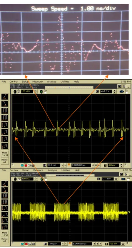
Fig. 20 The uncorrelated outputs of three adjacent channels
Data_In_Transmitter
Data_Out_Receiver
Fig. 21 The measured output at the receiver for radiated pattern from transmitter (data out is delayed and inverted)
Fig. 20. The uncorrelated outputs of three adjacent channels.
5 Experimental results
5.1 UWB transmitter
The UWB (6 GHz–8.5 GHz) transmitter has been imple-mented on 0.18µm CMOS technology, active area of 0.65 mm2. The power consumption is 0.6 m W for transmit-ting UWB pulses with on –off modulation keying at the data rate of 4 MHz. The die photo is shown in Fig. 17. The mea-surement of UWB transmitter, shown in Fig. 18, can be com-pared with the simulation results shown in Fig. 10
5.2 UWB receiver
The test structure has been implemented on 0.18µm CMOS technology, active area of 2.5 mm2. The UWB receiver, de-signed for maximum quench rate of 8 MHz, can receive max-imum data rate of 4MHz with power consumption of 2 mW
Fig. 20 The uncorrelated outputs of three adjacent channels
Data_In_Transmitter
Data_Out_Receiver
Fig. 21 The measured output at the receiver for radiated pattern from transmitter (data out is delayed and inverted)
Fig. 21. The measured output at the receiver for radiated pattern from transmitter (data out is delayed and inverted).
from 1.5 V supply. The die photograph is shown in Fig. 19. The adjacent frequency channels are placed far from each other to reduce the effect of coupling. The outputs of three adjacent channels, shown in Fig. 20, are uncorrelated to each other in the absence of UWB data, triggering only due to noise. Figure 21 shows the input data pattern to the trans-mitter. The transmitter generates pseudo random pattern of UWB pulses during low input level and off during is high in-put level. The peak voltage of these pulses is around 20 mV. The receiver input has been coupled to the UWB transmit-ter by a 60 dB attenuator. The output of UWB receiver aftransmit-ter statistical correlation of all channels is shown in Fig. 21.
6 Conclusions
The new architecture to receive the low power UWB pulse radio signals by statistical correlation of multiple channels has been proposed in this paper. The transmitter radiates pseudo random pattern of UWB pulse in the spectrum from 6–8.5 GHz. The receiver extracts the UWB pulses of energy level near to noise. Narrow band interfering transmitters are detected and eliminated by statistical correlation of twelve narrow bandpass SROs.
References
Baker,R. J., Li,H. W., and Boyce, D. E.: CMOS Circuit design, Layout, and Simulations, IEEE press series on Icroelectronics System, 1997.
Favre, P., Joehl, N., Vouilloz, A., Deval, P., Dehollain, C., and De-clerq, M.: A 2-V 600 uA 1GHz BiCMOS super-regenerative
304 M. Anis et al.: Design of UWB pulse radio transceiver using statistical correlation technique in frequency domain
ceiver for ISM applications, IEEE J. Solid- State Circuits, 33(12), 2186–2196, 1998.
Feick, R., Rojas, O., and Mackay, A.: Modeling and simulation of the super regenerative receiver, IEEE Trans. On Consumer Elec-tronics, 43(2), 92–102, 1997.
Jeong, Y., Jung, S., and Liu, J.: A CMOS impulse generator for UWB Wireless communication systems”, in proc. ISCAS, 129– 132 2004.
Joehl, N., Dehollain, C., Favre, P., Deval, P., and Declercq, M.: A low power 1-GHz super-regenerative transceiver with time-shared PLL control, IEEE J. Solid State Circuit, 36(7), 1025– 1031, 2001.
Moncunill-Geniz, F. X., P-Sch¨onw¨alder, P., and del Aguila- Lopez, F.: New superregenerative architectures for direct sequence spread spectrum communications, IEEE Trans. on Circuits and Systems-II Express Briefs, 52(7), 415–419, 2005.
Moncunill-Geniz, F. X.,P-Sch¨onw¨alder, P., and M-Casals, O.: A generic Approach to the theory of Super regenerative reception, IEEE Tran. on Circuits and Systems-I: Regular Paper, 52(1), 54– 70, 2005.
Maggio, G. M., Rulkov, N., and Reggiani, L.: Pseudo- chaotic time hopping for UWB impulse radio, IEEE Trans. On circuit and system-I, 48(12), 1025–1031, 2001.
Vouilloz, A., Declercq, M., and Dehllain, C.: A low power CMOS Super- Regenerative Receiver, IEEE J. Solid State Circuit, 36(3), 440–451, 2001.
Vouilloz, A., Declerq, M., and Dehollain, C.: Selectivity and sen-sitivity performance of super-regenerative receivers, in proc. IS-CAS’, 325–328 98.