Advances in Radio Science (2003) 1: 67–71 c
Copernicus GmbH 2003
Advances in
Radio Science
Modelling and characterization of a travelling-wave electro-optic
modulator on InP
W. Pascher1, J. H. den Besten2, D. Caprioli2, R. van Dijk3, X. J. M. Leijtens2, and M. K. Smit2 1Allg. und Theoretische Elektrotechnik, FernUniversit¨at, D-58084 Hagen, Germany
2Opto-Electronic Devices group, Eindhoven University of Technology, Eindhoven, The Netherlands 3TNO Physics and Electronics Laboratory, The Hague, The Netherlands
Abstract. A fast travelling-wave Mach-Zehnder modulator is modelled and designed using a rigorous vectorial analysis. In order to investigate propagation characteristics, velocity and microwave loss, the semiconductor layer stack and the lossy electrodes are modelled using the method of lines. The microwave field distribution is determined, design curves are derived and the cross-sectional dimensions of the modulator are optimized. The loss of the fabricated device agrees very well with small signal measurements up to 40 GHz and HFSS simulations.
1 Introduction
High speed modulators are of great interest for 40 Gb/s trans-mission systems and beyond. Travelling wave modulators (Walker, 1991) are not limited in frequency by the RC time constant. A Mach-Zehnder modulator has been realized, e.g., on GaAs (Walker, 1995) and on InP (M¨orl et al., 1999; Kr¨ahenb¨uhl, 1998). However, little is published about the microwave design considerations that are to be taken into account in the design of high-speed travelling wave Mach-Zehnder modulators on InP. Highly accurate design data are necessary for these devices because of the long and costly fabrication process. Hence a rigorous model is needed that includes the main limiting factors: the velocity mismatch be-tween the optical wave and the microwave as well as the mi-crowave loss.
The waveguide structure of the modulator considered here (Fig. 2) is composed of several semiconductor layers with a step index profile and lossy metallic electrodes. Conven-tional analyses use a model with homogeneous dielectric lay-ers and infinitely thin electrodes, which does not take the conductor losses into account. This yields an error in the mi-crowave phase velocity and an incorrect electric field. In this paper, the model used fully accounts for the microwave and
Correspondence to: W. Pascher
optical properties of the inhomogeneous layer stack. The loss in the modulating electrodes and in the semiconductor layers is considered by means of a complex dielectric constant.
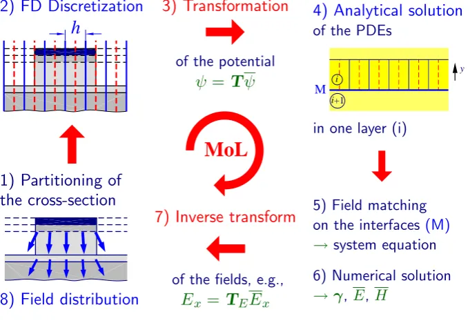
The model structure is analyzed by the method of lines (MoL), which has been efficiently used for the simulation of various planar waveguides for microwave integrated circuits and integrated optics (Pregla and Pascher, 1989; Rogge and Pregla, 1993; Pregla and Pascher, 1995). The MoL takes advantage of the planar layer stack by discretizing the wave equation in the direction parallel to the interfaces of the lay-ers, whereas an analytical solution is retained in the vertical direction. Thus highly accurate results are obtained at a com-paratively small numerical effort. In this paper, we present MoL simulations to optimize the electric field across the re-verse biased diode of the modulator. The results were con-firmed by HFSS (High-Frequency Structure Simulator) and by measurements.
1.1 Modulator layout and cross-section
Since a reverse bias is used and almost no current is flow-ing in InP-based Mach-Zehnder switches, they can operate at sub-nanosecond speed. If lumped metal contacts are used, i.e. on top of the interferometer arms and on the bottom of the chip, the optical bandwidth of the modulator is limited to a couple of GHz by the capacitance. In a travelling wave design, the capacitance is distributed along the line and is consequently no longer a bandwidth limiting factor. In an ideal design, the modulating microwaves are travelling along the phase-shifter with a low attenuation at the same speed as that of the optical waves.
68 W. Pascher et al.: Travelling-wave electro-optic modulator on InP MMI MMI +π in bar RF−out RF−in cross
Fig. 1. Top view of a travelling-wave electro-optic modulator. The
dashed line locates the cross-section of Fig. 2.
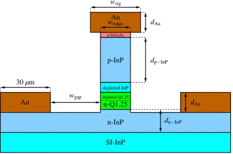
p-InP Au wsig dAu 30 µm wridge Au dAu dp InP dn InP wgap p-InGaAs n-InP SI-InP n-Q1.25 depleted-InP depleted-Q1.25
Fig. 2. Cross-section of a travelling-wave electro-optic modulator.
Therof InP/InGaAsP is 12.55 (the imaginary part is dependent on
the doping level).
p-doped layer. Due to the pin-structure of the optical wa-veguide, the microwave electric field needed for the electro-optic effect will be across the depleted region, which consists of the upper part of the film layer and the intrinsic layer.
2 Vectorial analysis by the method of lines
The analysis is based on the method of lines (MoL) as pre-sented in Pregla and Pascher (1989). The MoL is a semi-analytic approach with semi-analytic solution in one coordinate direction, namely perpendicular to the layers and a finite-difference discretization in the other direction. This ap-proach is very well suited for multilayered waveguides as, e.g., for the travelling wave modulator under consideration. The cross-section of a modulator (as in Fig. 2) is partitioned into an “arbitrary” number of layers. These layers are inho-mogeneous, also with permittivity steps (εr =εr(x)), dielec-tric loss (εr complex) and metallic loss (εr = −j
κ ωεo
). The wave equations are established using two scalar po-tentials ψe (electric) and ψh (magnetic). We obtain a Helmholtz- and Sturm-Liouville differential equation for each layer r(x) ∂ ∂x 1 r(x) ∂ψe ∂x +∂ 2ψ e ∂y2 +
r(x)k02−kz2
ψe=0 (1)
∂2ψh
∂x2 +
∂2ψh
∂y2 +
r(x)k02−k 2 z
ψh=0 (2)
where we have assumed wave propagation inzdirection ac-cording toψe,h∼exp(−j kzz).
The analysis steps of the method of lines for the electro-optic modulator are summarized in the flow chart (Fig. 3). We apply a finite difference discretization inxdirection in order to convert to partial differential equations to coupled ordinary ones. In this way we are able to obtain an analytical solution iny direction on discretization lines. Two sets of discretization lines are used, one for the electric potentialψe and the other for the magnetic oneψh. The first derivative with respect toxis expressed using finite differences and the following difference operatorD for the magnetic potential ψh ∂ψh ∂x
(i+1/2)h
≈ ψi+1−ψi
h or
h∂ψh
∂x → 1 −1 1
. .. . .. . .. . ..
−1 1
| {z }
D ψ1 ψ2 .. .
ψN−1
ψN
=Dψh (3)
The second derivative is given by
h2∂
2ψ h
∂x2 → −D tDψ
h= −Phψh
with tridiagonalPhand analogous for the electric potential ψe. This yields the discretized wave equation (a system of coupled ordinary differential equations)
d2 dy2ψh−
k2zI−εh+Ph
ψh =0 (4)
with a tridiagonal matrix Qh. In order to solve these equa-tions, we perform a diagonalization, namely by transforma-tion to principal axes:
T−1QT =02 (diagonal)
T−1ψ =ψ (5)
This constitutes two separate eigenvalue problems forψeand ψh. We end up with the transformed Helmholtz equation
d2 dy2ψ−0
2ψ =0 (6)
which is decoupled and has an analytical solution in each individual layer
ψ =exp(−0y)A+exp(0y)B (7) In the following process the tangential fields are matched on each layer interface and we obtain a formulation of an indi-rect eigenvalue problem
Z(εre)Ht an,M=0 (8)
W. Pascher et al.: Travelling-wave electro-optic modulator on InP 69
2) FD Discretization
h
x
z
y
I
II
I
III
I
II
I
III
II
I
MMPL108A
1) Partitioning of
the cross-section
8) Field distribution
3) Transformation
x z
y
I
II I
III
I II
I II III
I
MMPL108A
of the potential
ψ
=
Tψ
MoL
7) Inverse transform
x z
y
I
II I
III
I II
I
III II
I
MMPL108A
of the fields, e.g.,
E
x=
T
EE
x4) Analytical solution
of the PDEs
i+1
M
i
y
in one layer (i)
x
z
y
I
II
I
III
I
II
I
III
II
I
MMPL108A
5) Field matching
on the interfaces
(M)
→
system equation
6) Numerical solution
→
γ
,
E
,
H
Fig. 3. Flow chart of the analysis steps in the MoL.
−2 −1 0 1 2 3 4 5 6 7 8 9
−1 0 1 2 3
x [µm]
y [
µ
m]
Fig. 4. Microwave electric field (arrow width proportional to field) in the cross-section of the optimized modulator.
which is solved for the the effective permittivityεreby a nu-merical search for zeros. This also gives the electromagnetic field H, E in transform domain. Finally, an inverse transfor-mation yields the field distribution in the waveguide.
3 Simulation and measurement results
The modulator has been simulated by the MoL according to the cross-section in Fig. 2. First the field distribution is given. Then design curves with respect to various dimensions of the device are presented in order to optimize its performance. Fi-nally, the microwave loss and index are compared with small signal measurements and HFSS (High-Frequency Structure Simulator) simulations.
3.1 Field distribution
70 W. Pascher et al.: Travelling-wave electro-optic modulator on InP
0 0.5 1 1.5 2 2.5 3 0
1 2 3 4 5
α
[dB/mm]
d
Au [µm]
0 0.5 1 1.5 2 2.5 3 0
1 2 3 4 5
α
[dB/mm]
w
sig [µm]
0 0.5 1 1.5 2 2.5 3 0
1 2 3 4 5
α
[dB/mm]
w
ridge [µm]
Fig. 5. Attenuation at 40 GHz as a function of gold thickness thickness (left), signal line width (center), and p-cladding thickness (right).
Other parameters are as in the optimized design.
0
2
4
6
0
5 10 15 20 25 30 35 40
α
[dB/mm]
f [GHz]
0
2
4
6
8
10
0
5 10 15 20 25 30 35 40
Re(n
µ
)
f [GHz]
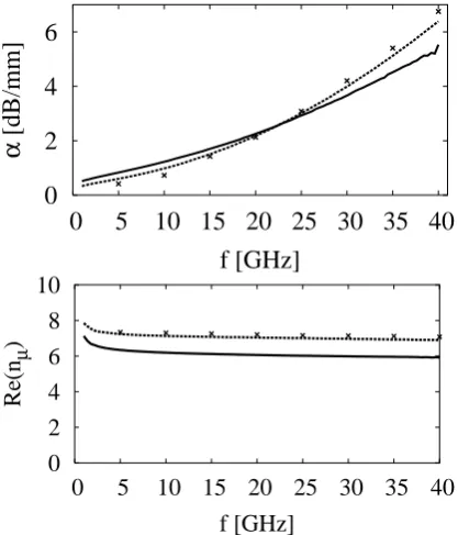
Fig. 6. Measurements (solid line), MoL-simulations (dashed line)
and HFSS-simulations (crosses) of the microwave attenuation α
(left) and the real part of the microwave index nµ(right) for a phase
shifter with a signal line widthwsigof 12µm.
3.2 Design curves
The biggest electro-optic effect will be obtained if the electric field is highest in the region where the light is confined. To make use of the pin-diode structure of the ridge, doping of the InP-ridge is necessary. Unfortunately, doped semiconductors have a conductivity that is much lower than that of metals. Therefore, the amount of doping in the cladding influences the RF-attenuation due to varying resistivity.
Figure 5 (simulated using the package MOLCAR; Kre-mer and Pregla, 1997) shows the attenuation is decreasing as the ridge width, and thus the amount of doped material in between the signal line and the depletion-zone edge, is
de-creased. Figure 5 also shows the effect of the shape of the signal line on the RF-attenuation. A wider signal line width reduces the RF propagation loss, because a bigger part of the electric field is concentrated in the air instead of the semicon-ductor material. The attenuation is also reduced if the gold thickness is increased. Since the skin depth of Au is about 385 nm at 40 GHz, especially at thin Au thicknesses the at-tenuation increases dramatically. All plots were simulated at 40 GHz.
3.3 Comparison with measurements
The optimized design as described in the previous sections, has not been fabricated yet. Therefore, we checked measure-ments on already existing modulators with simulations by the Method of Lines. The left part of Fig. 6 shows the attenuation data of a structure with a ridge width of 4µm and a signal line width of 12µm. The measured values for the phase-shifting section have been extracted using the thru-reflect-line (TRL) method (Enge and Hoer, 1979). Depicted are the values measured through small signal (SS-)measurements, calculated by the MoL and calculated by HFSS.
HFSS simulations have been performed using the same structure as for the MOLCAR simulations. HFSS (Ansoft) is a 3-dimensional finite difference EM field solver. The struc-ture is discretised in tetrahedra and the EM field components are calculated on the vertices and edges of these elements using appropriate boundary conditions. The mesh is refined adaptively at the locations where a large gradient exists. The output of a simulation is a.o. the impedance at the ports and the S-parameters. From these the complex propagation con-stant of the structure is calculated.
Comparison with measured values is very good. It can be noted that the loss curve does not follow a√f law, since the losses are mainly determined by the absorption in the sub-strate and not by the skin depth of the electrodes.
W. Pascher et al.: Travelling-wave electro-optic modulator on InP 71 materials considered. This is caused by the doped
semicon-ductor layers.
One of the causes for the offset between simulation and measurement of the effective index could be the lack of re-liable data of the used polyimide at RF-frequencies. Also, since the calculated values of the MoL and HFSS agree very well, we believe another source of error is the uncertainty of the doping levels in the different layers, which has not been measured. A different doping profile would not only change the conductivities, but also the thickness of the deple-tion layer. Attenuadeple-tion and effective index plots for a struc-ture with a signal line width ofwsig=6µm showed similar behaviour.
4 Conclusion
The method of lines (MoL) has been employed to model and design a fast travelling-wave electro-optic modulator. Field distributions and design curves have been presented and discussed in view of an optimized component with min-imum microwave loss. The small-signal measurements of the fabricated device show very good agreement (better than 0.5 dB/mm) with the MoL modelling and with HFSS simu-lation results.
Acknowledgements. This work has been carried out with the
par-tial funding of the European Union through the project IST 2000-25390 OBANET of the Information Society Technologies Research Programme and the Dutch NRC-Photonics programme.
References
Walker, R. G.: High-speed III-V semiconductor intensity modula-tors, IEEE J. Quantum Electron., 27, 3, pp. 654–667, Mar. 1991. Walker, R. G.: GaAs/AlGaAs travelling-wave modulators for mm-wave frequencies, IEE Colloquium Towards Terabit Transmis-sion, pp. 4/1–4/6, 1995.
M¨orl, L., Hoffmann, D., Matzen, K., Bornholdt, C., Mekonnen, G. G., and Reier,F.: Traveling wave electrodes for 50 GHz operation of opto-electronic devices based on InP, Proc. IPRM99 confer-ence, pp. 385–388, May 16–20 1999.
Kr¨ahenb¨uhl, R.: Electro-Optic Space Switches in InGaAsP/InP for Optical Communication, Hartung-Gorre Verlag, Konstanz, sec-ond edition, 202 pp., 1998.
Pregla, R. and Pascher, W.: The Method of Lines, in T. Itoh (ed.): Numerical Techniques for Microwave and Millimeter Wave Pas-sive Structures, New York, USA, J. Wiley Publ., pp. 381–446, 1989.
Rogge, U. and Pregla, R.: Method of Lines for the Analysis of Di-electric Waveguides, J. Lightwave Technol. 11(12), pp. 2015– 2020, 1993.
Pregla, R. and Pascher, W.: Vectorial Analysis of Optical Wave-guides by the Method of Lines, in Annual Review of Progress in Applied Computational Electromagnetics (ACES), 11, Mon-terey, USA, pp. 943–950, 1995.
Kremer, D. and Pregla, R.: MOLCAR a Very Efficient and Accu-rate Design Tool for the Hybrid Analysis of Multilayered Wave-guide Structures, in Proc. SPIE Photonics West, Integrated Op-tics Devices: Potential for Commercialization, San Jose, USA, vol. 2997, pp. 255–262, Feb. 1997.