Nanotechnology based Effective Design Approach for
Code Converter Circuits using QCA
P.Ilanchezhian
Associate Professor Department of IT Sona College of Technology
R.M.S.Parvathi,
PhD. PrincipalSenguthar College of Engineering Tiruchengode
ABSTRACT
A scheme for reducing the number of cells in Quantum dot Cellular Automata circuit is presented. In this paper, an effective approach to analysis and design of code converter circuit using quantum dot cellular automata is explored in nanotechnology. This paper three input majority gate is the fundamental component of the QCA circuit implementation. It provides a considerable reduction in hardware cost compared to the other accessible methods. All other type of combinational circuits like adder, subtractor, decoder, and encoder etc can be constructed by the three input majority gate circuit only. The proposed code converter circuit is designed and replicated using quantum dot cellular automata designer tool for the four input levels. Finally, these proposed QCA circuits are compared with the other established and conservative circuits in terms of area and cell counts.
Keywords:
Code converter, Digital Circuits, QuantumDot Cellular Automata, Majority gate, minterm generator.
1.
INTRODUCTION
Logic circuits for digital systems may be combinational digital circuit or sequential digital circuits. A combinational circuit is represented with logic gates whose outputs at any occasion are computed from only the current combination of input levels. A combinational circuit performs a function that can be indicated understandably by a set of Boolean functions. In conservative Complementary Metal Oxide Semiconductor technology, designers come across the physical limit, high power consumption and low speed. Because of these failures, they have switched to the new nanotechnologies such as Single Electron Transistor, Carbon nano tube and Quantum-Dot Cellular Automata [1]. Operations in QCA are evaluated based on Columbic interaction as a replacement for current used in Complementary Metal Oxide Semiconductor technology, so there is no leakage current. Using this latest technology, Quantum-Dot Cellular Automata gives important features such as low power consumption, quick switching speed and small dimensions. The basic element in QCA is a squared cell that consists of four dots positioned at the corners and two free charges. Because of Columbic communications between electrons in Quantum Dots of a cell, two stable polarizations is generated, which are determined to logic “0” and logic “1” [1],[2]. QCA is a binary logic architecture which encodes binary information using two polarizations. Two fundamental logic structures for QCA are the inverter and the majority gate
[1]–[3]. A large amount of design projects on QCA circuit designs have been proposed based on two cell inverters and three input majority gate elements [4]-[7]. A new effective design approach for QCA circuit is presented in this paper. The natural quantum actions of a QCA cell provide a strong method for designing QCA circuits. In this approach, the arbitrary Boolean function is designed by utilizing the correct arrangement of cells based on Columbic interaction. The remaining part of the paper is ordered as follows. Section 2 is committed to explain the basic concepts of QCA. The proposed approach is represented in section 3 and its corresponding QCA implementation is presented in Section 4. Then simulation results and comparisons are explained in the next section. Finally this paper is concluded in section 6.
2.
QCA FUNDAMENTALS
The circuit designers need a more accurate simulation and design layout tool to determine the functionality of QCA circuits. QCA designer tool is the important publicly available design and simulation tool for QCA. It is developed at the ATIPS Laboratory, at the University of Calgary, QCA Designer currently supports three different simulation engines, and many of the CAD features required for complex circuit design. The first is a digital logic simulator, which requires cells to be either null or fully polarized. The second is a nonlinear approximation engine, which uses the nonlinear cell-to-cell response function to iteratively determine the stable state of the cells within a design. The third uses a two-state Hamiltonian to form an approximation of the full quantum mechanical model of such a system.
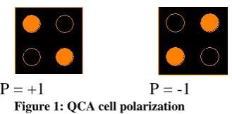
P = +1
P = -1
Figure 1: QCA cell polarizationQCA wire helps in propagation of logic levels with help of electrostatic repulsion and not current flow. In a QCA wire, the binary signal propagates from input to output because of the electrostatic interactions between cells [8],[9].
The structure of the QCA inverter is usually formed by placing the cells with only their corners touching. The electrostatic interaction is inverted, because the quantum-dots corresponding to different polarizations are misaligned between the cells [9].The majority gate produces an output that reflects the majority of the inputs. The QCA majority gate has four terminal cells out of which three are representing input terminal cells and the remaining one represents the output cell.
[image:2.595.78.243.69.150.2]
Figure 2. 1: QCA majority gate
Figure 2.2: Majority gate Symbol
A most fundamental QCA majority gate is shown in Figure 2. The propensity of the majority device cell to move to a ground state ensures that it takes on the polarization of the majority of its neighbours. The device cell will tend to follow the majority polarization because it represents the lowest energy state. To produce well-organized QCA design, the digital circuits are implemented with the help of majority gate-based design techniques are needed. [10].
3.
CODE CONVERTER CIRCUIT
A binary code is a group of n bits that assumes up to 2n distinct combinations of one’s and zero’s, with each combination representing one element of the set that is being coded. Discrete quantities of information are represented in digital systems by binary codes. The availability of a large varity of codes for the same discrete elements of information results in the use of different codes by different logical digital systems. Sometimes it is necessary to use the output of the one system as applied to the input to another system. A conversion circuit must be inserted between the two systems if each uses different codes for the same information. A code
converter is a combinational circuit that that makes the two systems compatible even though each uses a different binary code. To convert from one binary code X to another binary code Y, the input lines must supply the bit combinations of elements as specified by code X and the output lines must be generate the corresponding bit combinations of code Y. A combinational logic circuit performs this transformation with the help of logic gates.
In order to design a combinational logic circuits first form the specifications of the circuit, determine the required number of input levels and output levels and assign a specific symbol to each levels. After that derive the function table that defines the required relationship between input and outputs. Then obtain the simplified Boolean function for each output as a function of the input variables. Finally draw the logic diagram and verify the results of design by simulation. The Karnaugh map is providing a simple procedure for simplifying the given Boolean function. This method provides a pictorial form of a function table. A Karnaugh map is a diagram and it is made up of squares with each square represent a min term of the function that is to be simplified. Consider a new procedure for understanding and reduce the logical operations in the form of Majority of majority functions. In each square that has a Boolean variable one value represent that was11-, and the square with Boolean 0 will be represent the value 00- to produce a new map method that will be pointed to as J-map denoting majority function. To designate the four binary input variables by b1, b2, b4 and b8 and the four output variable by g0, g1, g2 and g3. Here four input binary variable may have 16 bit combinations. In order to obtain the simplified Boolean functions for the outputs better use J map instead of K map. There are four map represents four output levels of the circuit as a function of the four input variables. A two level logic diagram may be obtained directly from the Boolean expressions derived from the map.
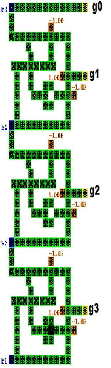
4. QCA IMPLEMENTATION
Figure 3. QCA implementation of four bit binary to gray code converter circuit
[image:3.595.285.505.92.706.2]5. SIMULATION RESULTS
[image:4.595.316.510.130.503.2]The combinational code converter circuit functionality is verified using QCA Designer tool ver.2.0.3. The simulated waveforms of combinational four bit binary to gray code converter circuit and four bit gray to binary code converter circuits are shown in Figure 5 and Figure 6 respectively. The code converter circuit has four clocking zones. Initially clock 0 is used to get the inputs A and B. Clock 1 is used to route inputs for majority gate logic, clock 2 is used for finding majority logic and clock 3 is used to compute output. The output is available at clock 0 again. Clock 1 to 3 considered here is a sequence of setup for hold, relax and release phase, to control the flow of information in QCA circuits. Similarly, to design different combinational generator circuit also need 4 clock zones are used to produce required output..
Figure 5.Simulation result of four bit binary to gray code converter circuit
Figure 6.Simulation result of four bit gray to binary code converter circuit
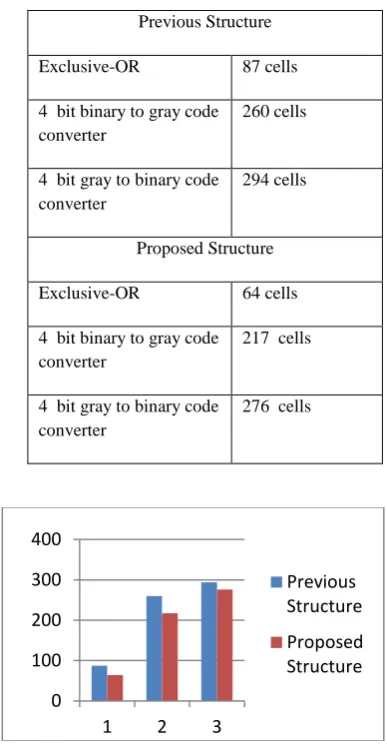
The proposed QCA code converter circuit designs are compared with the conventional circuit structures with the help of Table 1 and Figure 7.
Table 1. Number of QCA cells
[image:4.595.68.269.261.437.2]
Figure 7.QCA cell count comparison for previous and proposed Structures
In Figure 7, the number 1 in x axis indicates the fundamental EX- OR gate and number two indicates four bit binary to gray code converter circuit and number three indicates four bit gray to binary code converter circuit. Proposed structure Exclusive OR gate needs only 64 QCA cells. The four bit binary to gray code converter and four bit gray to binary code converter circuit is implemented with Exclusive OR gate. It can be clearly apparent that this approach can be simplified and optimized compared to conventional circuit designs in terms of number of cell counts, area, and complexity
6. CONCLUSION
A novel effective method for designing QCA circuit has been presented in detail. The proposed approach design results in the reduction of the number of cells considerably lower than number of cells and smaller area compared to the conventional CMOS technology. The operation of the proposed QCA three input majority gate
0 100 200 300 400
1 2 3
Previous Structure
Proposed Structure Previous Structure
Exclusive-OR 87 cells
4 bit binary to gray code converter
260 cells
4 bit gray to binary code converter
294 cells
Proposed Structure
Exclusive-OR 64 cells
4 bit binary to gray code converter
217 cells
4 bit gray to binary code converter
[image:4.595.59.256.491.684.2]architecture has been described and simulated using the QCA designer simulator tool. The simulation results for four bit binary to gray code converter and four bit gray to binary code converter have been presented. The designed QCA based combinational code converter circuit can be used to represent only four input levels and generate only four output levels. In future, this can be extended to represent higher input and output levels.
7.REFERENCES
[1] C. S. Lent, P. D. Tougaw, W. Porod, and G. H. Bernstein, “Quantum cellular automata.”, Nanotechnology, vol. 4, no. 1, pp. 49-57, January 1993. [2] P.D. Tougaw, C.S. Lent, “Dynamic behavior of quantum
cellular automata”, Journal of Applied Physics 80 (8) (1996) 4722–4736
[3] Lent, C.S.; Tougaw, P.D.; , "A device architecture for computing with quantum dots," Proceedings of the IEEE , vol.85, no.4, pp.541-557, Apr 1997.
[4] Cho, H.; Swartzlander, E.E.; , “Adder Designs and Analyses for Quantum-Dot Cellular Automata,” Nanotechnology, IEEE Transactions on , vol.6, no.3, pp.374-383, May 2007.
[5] K. Navi, S. Sayedsalehi, R. Farazkish, M.Rahimi Azghadi, “Five-input majority gate, a new device for quantum-dot cellular automata”, Journal of
Computational and Theoretical Nanoscience, vol.7, pp. 1546-1553,2010.
[6] S. Sayedsalehi, M. H. Moaiyeri and K. Navi, “Novel Efficient Adder Circuits for Quantum-Dot Cellular Automata”, Journal of Computational and Theoretical Nanoscience, vol. 8, pp. 1769-1775, 2011.
[7] Zhang Rumi, K. Walus, Wang Wei, and G. A. Jullien , “Performance comparison of quantum-dot cellular automata adders,” in Circuits and Systems, 2005. ISCAS 2005. IEEE International Symposium on, 2005, pp. 2522-2526
[8] Heumpil Cho, Student Member, and Earl E. Swartzlander, Jr., Fellow, IEEE. “Adder Design and Analyses for Quantum-Dot Cellular Automata”, IEEE Trans. Nano., Vol.6, No.3, may 2007.
[9] K. Walus, G. Schulhof, G. A. Jullien, R. Zhang, and W. Wang, “Circuit design based on majority gates for applications with quantum-dot cellular automata,” in Conf. Rec. 38th Asilomar Conf. Signals, Systems and
Computers, 2004, vol. 2, pp. 1354–1357.