Effect of Mass Fraction of Ni in Solution on the
Microstructure and Sensitivity of Cu/Ni Film as
Low-Temperature Sensor
Moh. Toifur
*, Azmi Khusnani, Okimustava
Department of Physics Education, Ahmad Dahlan University, Indonesia
Received July 30, 2019; Revised October 8, 2019; Accepted December 10, 2019
Copyright©2019 by authors, all rights reserved. Authors agree that this article remains permanently open access under the terms of the Creative Commons Attribution License 4.0 International License
Abstract
The purpose of this research is studying microstructure, the resistivity of Cu/Ni film produced by electroplating on the various mass fraction of Ni in the electrolyte. Then the film is tested for its performance as a temperature sensor. The electrolyte solution was made from mixing of NiSO4, NiCl2, H3BO3, and H2O. Plating was conducted on power 1.5 V and 60°C bath temperature. The results showed deposits containing Ni and NiO. The X-ray diffraction parameters of Ni[111] and NiO[111] such as intensity, d-spacing and grain size on variations of Ni mass fraction in solution followed the parameters diffraction of Cu[111]. The resistivity is contributed by competition between those three diffraction parameters. Testing Cu/Ni films for sensing the temperature of liquid nitrogen (0°C to -140°C) shows that all samples have exhibited their performance as low-temperature sensors. The temperature has a linear relationship to the output voltage of the sensor with the sensitivity ranging from 0.7510-3 V/°C to 1.0510-3 V/°C. The highest sensitivity in accordance to the sample produced from 8.83 g Ni in the electrolyte.Keywords
Electroplating, Low-Temperature Sensor, Mass Faction of Ni, Microstructure, Sensitivity1. Introduction
Copper and nickel were known as materials that can be used as temperature sensors from 400C to -234.5C [1,2], having a high-temperature coefficient of resistance reaching 4300 ppm/C [3]. Although the quality is not as good as Pt by combining or alloying both materials, it can overcome the deficiency against Pt, even Cu/Ni or CuNi can be used as cryogenic sensors. High stability and sensitivity are the advantages of temperature sensor from the combination of Cu and Ni.
Electroplating is a good method in growing Ni film on Cu substrates to form Cu/Ni [3]. Its advantages are known from the good adhesion between Cu and Ni [1], [4, 5]. The advantage of electroplating is well known due to the simplicity of the method, low cost [6], highly productive, and the results are competitive [7, 8], and readily adoptable [9].
Several factors determining the success of electroplating include pH, electrolyte solution temperature [10], bath concentration, metal ion, plating time, agitation [11]. Here, pH is used to control the rising hydrogen gas, the bath temperature is used to determine the viscosity of the solution. The more dilute the solution the easier the ion penetrates the solution toward the cathode to form a deposit. The electrolyte concentration determines the number of particles that are possible to be ionized, and deposition time determines the thickness of the film. The presence of agitator will make the combination between elements of solute easier.
In relating to electrolyte concentration, according to Faraday's law, it is known that the number of deposited particles is proportional to the concentration of particles in solution [12, 13, 14]. There are some researchers who claim that there is actually no effect of concentration on the rate of deposit formation because the increasing concentration will reduce the resistivity of the solution so that the voltage also decreases. With decreasing the voltage, the production of deposit decreases. By taking this consideration, the increasing concentration must be considered by the driving voltage of the ionic particle in the solution. If the driving voltage is able to ionize the particles, the mobilization of the ions leading to the cathode also increases so that it will accelerate the formation mechanism of deposits.
temperatures from 0C to -200C was studied. We wish variation of nickel mass fraction in solution will influence the thickness of Ni in Cu substrate so the actual research really on the influence of size effect on the several quality parameters of the thermal sensor [15].
2. Experimental
A commercially available copper plate with the dimension of 0.3 mm 1.0 1.3 cm2 was used as the substrates and will be set as a cathode. For preparing copper as a cathode material, it was successively finned by metal polish, brushed with detergent, rinsed at first by distilled water, and then by alcohol 95% in ultrasonic cleaner during 6 minutes. Subsequently, substrate was hair dried, wrapped by tissue paper and saved in a storage box. Nickel plate with the same size as copper also was given the same treatment as in copper, and was set as an anode.
The boric acid (H3BO3), nickel sulphate (NiSO4), nickel chloride (NiCl2), and distilled water were prepared to make electrolyte material. The electrolyte concentration was varied by varying the nickel content in solution. Detail elements and these amounts were listed in Table 1. There are two entities that do not change i.e. mass of H3BO3 (7.5 g), volume of destilled water H2O (250 ml).
Table 1. Samples on the various electrolyte concentration
Mass of NiCl2 (g) Mass of NiSO4 (g)
Mass of Ni in solution (g) Mass fractionof Ni (%) Name of sample
10 75 33.09 9.66 S1
15 100 44.87 12.05 S2
20 125 56.66 14.08 S3
25 150 68.44 15.82 S4
30 175 80.23 17.35 S5
Boric acid was used to control the electrolyte PH. The suitable pH on nickel solution was ranging from 2 up to 4 [16]. Nickel chloride was varied to control electrolyte conductivity and corrosion speed on the anode, and nickel sulphate was used to control current density.
All materials were mixed in beaker glass and stirred by Magnetic stirrer MS 200 during 2 hours to reach a homogeneous solution. Electroplating was done in the setting parameter as listed in table 2.
Table 2. Parameter setting for electroplating process
Electrolyte volume 300 ml
Electrolyte temperature 60C
Electrolyte volume 300 ml
Time deposition 60 s
Electrodes distance 4 cm
Current density 0.12 A/cm2
Electrolyte PH 4.2
Several characterizations have been done including the presence of Ni particles and it content studied by SEM photograph both of surface and cross-section and accompanied by EDX. In this case, we take two samples that are S1 and S5. From differences of mass fraction of Ni in the two samples, the thickness of the effect of concentration to the Ni content could be known. Then we used Ohaus balancing type PA214 to obtain the mass fraction of samples. Weighing the sample before and after Ni plating the thickness of Ni film could be determined through formula, Cu/Ni Ni Cu m m A
(1)
where is the thickness of Ni film, mCu/Ni is the mass of Cu/Ni, and mCu is mass of Cu substrate, Ni density od nickel, and A is the surface area. Furthermore, the microstructure of the sample was studied from XRD. From X-ray diffractogram, we are able to know the crystallinity of Ni film and the ordering level of crystalline structure. Also through Scherrer formula, the grain size could be obtained. After we study the microstructure of Ni deposit we obtain the sheet resistivity of Cu/Ni using a four-point probe. From sheet resistivity, we make an analysis of its relation to microstructure of deposit. Performance of the sensor was given from resolution of the sensor that was studied from the output voltage of sensor versus ambient temperature. According to the criteria of temperature sensor ranging from -200C to 0C as revealed by Rupin and Polak [12], the relationship between resistance (Rtd)
and temperature (T) follows polynomial order-3 of temperature.
3
0
( ) i
td i
i
R T k T
(2)Since data acquisition of resistance Rtd is represented by
a voltage of sensor V which is proportional to R, then in eq. (1) we can eliminate Rtd(T) by V(T) to give,
3
0
( ) i i
i
V T c T
(3)Then c1 is coefficient of 1st order polynomial that revealed the resolution of the sensor. The less the power of polynomial the more qualified the sensor. By comparing values of c1 in each sample, the most sensitive sensor to response the temperature changes can be obtained.
3. Result and Discussion
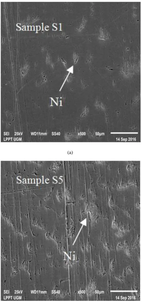
[image:2.595.61.288.651.753.2]can be seen that Ni particles have attached to the Cu substrate. Besides that, the surface density of Ni particles on sample S5 is more than that on sample S1. Again, the particle size on S5 is greater than that in S1. It is suitable with the character of NiCl2 in the electrolyte that can be rising the conductivity. As a result, the amount of Ni ions leads to cathode increases in line with increasing the number of Ni in electrolyte. This can accelerate the formation of Ni film in Cu substrate from particles to clusters, from clusters to islands, and then become continuing layer [9]. This happens continuously and repeatedly to form the film with the thickness that is proportional to the deposition time.
(a)
(b)
(c)
(d)
Figure 1. Micrograph of surface and cross section of Cu/Ni for sample S1 and S5
[image:3.595.62.289.242.729.2]Table 3. Comparison between copper and nickel on the Cu/Ni film
Mass percentage of Sample S1 Sample S5
Ni 9.27% 22.35%
Cu 70.47% 57.16%
We also calculated the thickness of Ni film from Ni mass data before (MCu) plating and after plating (MCu/Ni) by referring to eq. (1). The result is shown in Table 4.
Table 4. The thickness of Ni film on various electrolyte concentrations
Mass of Ni in the electrolyte (g)
MCu
(g)
MCu/Ni
(g)
The thickness of Ni film (m)
33.09 3.1796 3.1802 0.50
44.87 3.0950 3.0957 0.52
56.66 3.2145 3.2152 0.54
68.44 2.9739 2.9746 0.56
80.23 3.0234 3.0241 0.58
The table enables to support explaining the micrograph of Cu/Ni cross section as exhibited in Fig 1(c) and Fig 1(d) more detail. Sequence data of thickness revealed that the increasing mass fraction of Ni in the electrolyte has a relationship with an increasing of the thickness of Ni film. The relationship of mass fraction of Ni in electrolyte (m) toward the thickness of the Ni film according to the equation
3
1.84 10 m 0.44
(m) (4) where m is the weight of Ni. By referring to Marshal [17] revealed the 250 nm is the minimum thickness for the thermal sensor that is possible to reach the maximum power, all samples have exceeded the limit of thickness. Therefore, all samples have the possibility to be used as a material of sensor.
Furthermore, in Fig. 2, X-ray diffractogram is displayed. The sample forms polycrystalline containing 3 phases that are Ni, Cu, and NiO. The position of predominant peaks was located at 2 of about 39.0 for Ni (111), 41.5 for NiO (111), and 43.5 for Cu (111). In here, the presence of NiO phase was originated from H2O that resolved at the anode to be H+ and O2. A part of O2 will react with Ni to form NiO. NiO is transition metal oxide that is able to be used as thermal absorber [18]. Therefore, in the following description, NiO was included together with Ni.
20 30 40 50 60 70 80 90 100
0 4000 8000 12000 16000 20000 24000 28000 32000
38 39 40 41 42 43 Cu(211)
+
o
Cu(210) o: NiO(111) x: Ni(111)
+: Cu(111)
S5 S4 S3 S2
Intens
ity (a.u.)
2 Theta (deg.)
S1
x
o x
Figure 2. X-ray diffraction for sample Cu/Ni films in the various mass fraction of Ni
The mass fraction of Ni in solution influences the intensity of diffraction and the shifting of the predominant peak of a diffraction angle (as shown in the subplot). From Bragg formula, the change of diffraction angle will change the interplanar spacing. A shift to the right will reduce the interplanar spacing. This will affect the conductivity of the material in that direction which is becoming more conductive. Again, from the Scherrer formula for the right shifting of the diffraction angle, the particle size becomes larger.
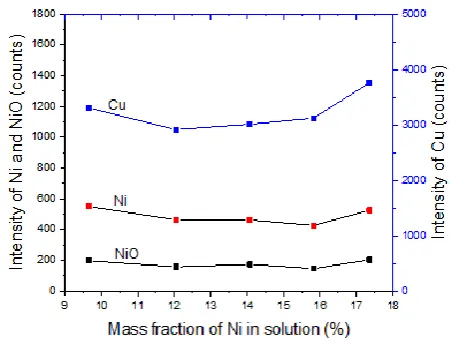
The intensity of diffraction angles was changed according to the change of mass fraction of Ni, as shown in Fig. 3.
[image:4.595.310.527.85.233.2] [image:4.595.59.289.93.147.2] [image:4.595.60.288.212.323.2] [image:4.595.308.534.439.608.2]Cu as a substrate has a diffraction intensity pattern as shown in Fig. 3. The various intensities are related to the surface condition of the Cu substrate. Then when Ni and NiO were grown on Cu substrate which has the pattern of diffraction as described in Fig. 3, it turns out that Ni and NiO follow epitaxially to the Cu pattern. The variation of mass fraction of Ni in solution only slightly affects the intensity of Ni and NiO. At the S3, the intensity of the two phases rises rather different from the intensity of Cu that is relatively straight from S2 to S4. At S5, concentrations of both Ni and NiO have been readjusted to the intensity pattern of Cu that rises up to almost the same as the intensity on S1.
In Fig. 4, the interplanar spacing of the Ni lattice and NiO particles is shown.
Figure 4. Interplanar spacing of Ni and NiO in the various weight of Ni in the electrolyte
Both d-spacings of Ni and NiO parallel each other. At S1 position of Ni at the angle of 2 = 39.03 with d-spacing for Ni is 2.31Å while d-spacing for NiO at the angle 41.50 is 2.17Å. This is the highest d-spacing compared to the other even though the difference is small enough that is 0.01 Å. When the concentration is increased as shown at S2 the
d-spacing drops from 2.31Å to 2.29Å for Ni and from 2.17 Å to 2.16Å for NiO. It is estimated that at this concentration Ni atoms are well attached to the Cu and orderly arranged in the direction (111) so the interplanar spacing becomes minimum. However, when the concentration is raised to product S3 up to S5 the d-spacing gradually rising up to 2.30Å for Ni and 2.17 Å for NiO.
In line to the increasing electrolyte concentration, the number of Ni ions gets larger so the atomic arrangement of Ni and NiO is not as good as at these in S2. In this case, debit of incident Ni ions which are able to be captured by the cathode surface Cu exceeds the capacity so that after capturing electrons to become Ni atoms, the Ni atoms cannot be arranged properly. Consequently, the interplanar spacing becomes larger. We can also see the diffraction intensity in Fig. 4 for both Ni and NiO, both of which fall
from C2 to C4.
The effect of the mass fraction of Ni to the grain size was displayed in Fig. 5. Here, grain size (GS) was calculated by Scherrer formula using X-source CuK, = 1.5419 Å.
Figure 5. The grain size of Ni and NiO
The grain size depends on two things, namely the diffraction angle and FWHM. From sample S1 to S2, diffraction angle (2D) was shifted to the right, then
gradually getting left on S5 which has a diffraction angle still greater than that on S1. Similarly, FWHM gradually increases from S1 to S4 then decreases on S5 which is almost the same to the FWHM on S1. The combination of both 2D and FWHM influences the grain size to decline
from S1 until S4 then rises on S5. But in general, it appears that the pattern of grain size curves for Ni and NiO relatively follows the diffraction peaks intensity pattern of Cu.
The relation between sheet resistivity (Rs) and the mass
fraction is given in Fig. 6. The value Rs depends on grain
size and interplanar spacing (d-spacing). Sometimes interplanar spacing dominates the Rs while grain size is not
or vice versa.
Figure 6. The sheet resistivity Cu/Ni
[image:5.595.311.532.139.325.2] [image:5.595.63.286.269.448.2] [image:5.595.310.532.571.716.2]contributed by grain size and d-spacing. The grain size (GS) contributes inversely proportional to Rs (~ 1/GS) [20],
while d-spacing gives the contribution proportional to the
Rs. But S1 value Rs was dominated by d-spacing so that the
large of grain size did not make Rs become small but follow
a large d-spacing. S5 the value Rs decreases. Decreasing Rs
is predominantly contributed by grain size rather than
d-spacing due to the high concentration of Ni in the deposit that makes the boundaries between grains that are previously built become connected.
It is known that among the use of Ni is increasing the resistivity of Cu. Considering resistivity of nickel and copper is 7.3 cm 1.7 cm respectively [21] then plating Ni to Cu will increase the resistivity. But there are things that should not be forgotten, which is the ordering atomic structure in a material. The ordering of the microscopic structure of the material is characterized by
d-spacing and grain size through X-ray diffraction. In this study, it was apparent that the microstructure plays an important role in determining Rs.
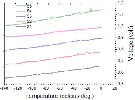
Furthermore, one indicator of the sensor quality is sensitivity. For the temperature sensor, the sensitivity was determined from the change of voltage as a representation of the change of resistivity in responding to the change of medium temperature. Liquid nitrogen filled in the flask was used as medium temperature. From the top of the flask to the bottom the temperature gets lower from -40C to -200C. The sensor was lowered slowly from top to bottom in such a way that the non-linear voltage-temperature gradient effect can be avoided [22]. The speed of the sensor in moving down was 0.17 cm/s while the sampling rate was set on 2 samples/s. The relationship between temperature and voltage graphically was given in Fig. 7.
Figure 7. Voltage-temperature relationship to indicate the sensitivity of sensors
All of the samples have exhibited a strong tendency to follow a linear regression to temperature. This is the simplest form of the relationship between resistance and temperature in a kind of Resistance Temperature Detector (RTD) [23, 24]. Equations that state the relationship
between V and T are given in Table 5, where intercept and slope of the graph are in accordance with coefficient c0 and
c1 in eq. (3). Determination index which is about 0.99 indicates this.
Table 5. Relationship between voltage and temperature in various samples
Samples Equation V=c0+c1T (volt)
Determination index (R2)
S1 V = 0.6510 + 0.00075T 0.99
S2 V = 0.6115 + 0.00085T 0.98
S3 V = 0.6396 + 0.00079T 0.99
S4 V = 0.6908 + 0.00063T 0.99
S5 V = 0.6311 + 0.00105T 0.99
The level of linearity of curve indicated by the determination index is one indicator of a good sensor. The power in the equation has already less to the maximum power required for the low-temperature sensor that is 3 [19]. Sensitivity was found through the value of c1 as coefficient T. Sensitivity ranges from 0.7510-3 V/C to 1.0510-3 V/C. The greater the c1 is,the more sensitive the sensor is. The highest coefficient is in accordance with S5 that is 0.001 V/C or exactly (1.05 0.01)10-3V/C. The pattern of sensitivity was given in Fig. 8.
Figure 8. The sensitivity of the sensor at the various mass fraction of Ni
[image:6.595.305.539.159.254.2] [image:6.595.309.534.390.574.2] [image:6.595.63.286.486.651.2]temperature correlates with the value of R(T) and the change in temperature will change the value of R(T). Electric current through R(T) will produce voltage depending on temperature V(T). S5 is the easiest sample to respond to changes in ambient temperature compared to others so that it has the highest sensitivity.
4. Conclusions
The plating of Ni on Cu substrate by varying the mass fraction of Ni in solution influences the thickness of Ni film, microstructure, and sensitivity of Cu/Ni as a low-temperature sensor. The thickness of Ni is proportional to the electrolyte concentration. From analysis on resistivity obtained information resistivity of Cu/Ni depends not only on the thickness of the Ni film but also on the regularity of the crystal and grain size. All samples can be used as low-temperature sensors to measure temperatures from 0C to -140C. Sensitivity is a linear relation to ambient temperature where S5 has the highest sensitivity that is 1.0510-3 V/C.
Acknowledgments
This research is a part of main research according to an improvement of the quality of low-temperature sensor through a synthesis of Cu/Ni thin film assisted magnetic fields. The researcher expresses his deepest gratitude to the Ministry of Research, Technology and Higher Education of the Republic of Indonesia which has provided research funding through the 2019 Higher Education Advanced Applied Research (PTUPT) scheme.
REFERENCES
[1] Afsarimanesh N & Zaheer AP, “LabVIEW Based Characterization and Optimization of Thermal Sensors”. International Journal on Smart Sensing and Intelligent Systems, Vol. 4 No. 4, (2011), pp. 726-739.
[2] Yang L, Zhao Y, Feng C, Zhou H., “The Influence of Size Effect on Sensitivity of Cu/CuNi Thin- film Thermocouple”, Physics Procedia, Vol. 22, (2011), pp. 95-100
[3] Lukose CC, Zoppi G & Birkett M, “Thin film resistive materials: past, present, and future”, Materials Transactions, Vol. 45, No. 12, (2004), pp. 3330 to 3333.
[4] Ralph H. Fundamental of Physical Metallurgy. Prentice-Hall Inc. (1953).
[5] Okamoto N, Wang F & Watanabe T, Adhesion of Electrodeposited Copper, Nickel and Silver Films on Copper, Nickel and Silver Substrates, Materials Transactions, Vol. 45, No. 12 (2004), pp. 3330 to 3333.
[6] Boylestad, Introductory Circuit Analysis, Tenth Edition. Parential Hall Pearson Education International (2003).
[7] Srinivas P, Hamann S, Wambach M, Ludwig A & Dey SR, “Fabrication of a Ni-Cu Thin Film Material Library Using Pulsed Electrodeposition”, Journal of the electrochemical society, 161 No. 10 (2014), pp. 504-509).
[8] Donald MM, Handbook of Physical Vapor Deposition (PVD) Processing Film Formation, Adhesion, Surface Preparation and Contamination Control, New Jersey: Noyes Publications, (1986).
[9] Grujicic D., Pesic B., “Electrodeposition of copper: the nucleation mechanisms”, Electrochimica Acta 47, (2002), pp. 2901-2912
[10] Luo JK, Pritschow M, Flewitt AJ, Spearing SM, Fleck NA & Milne WI, “Effects of Process Conditions on Properties of Electroplated Ni Thin Films for Microsystem Applications”, Journal of The Electrochemical Society, 153(10), (2006), pp. 155-161.
[11] Kumar S, Pande S & Verma P, “Factor Effecting Electro-Deposition Process”, International Journal of Current Engineering and Technology, Vol.5, No.2, (2015), pp. 1- 4.
[12] Guler SE., Karakaya, Konca E, “Effects of current density, coating thickness, temperature, pH and particle concentration on internal stress during Ni–MoS2 electroco deposition”, Surface Engineering, Vol 30, No.2, (2014), pp. 109-114.
[13] Chang YC, Chang YY, Lin CI, “Process Aspects of the Electrolytic Codeposition of Molybdenum Disulfide with Nickel”, Electrochimicia Acta. Vol. 43, No. 3-4, (1998), pp. 315-324.
[14] Huang ZJ, Xiong DJ MoS2, “Coated with Al2O3 for Ni-MoS2/Al2O3 Composite Coatings by Pulse Electrodeposition”, Surface Coatings Technology. Vol. 202, No. 14, (2008), pp. 3208–3214.
[15] Cattani M, Salvadori MC, Vaz AR & Teixeira FS, “Thermoelectric power in very thin film thermocouples: Quantum size effects”, Journal of Applied Physics, Vol. 100, No. 11, (2006), pp. 4905-4909.
[16] Tokarz, Frączek T, Bałaga Z & Nitkiewicz Z, “Structure, hardness and thermal stability of electrodeposited Cu/Ni nanostructured multilayers”, Rev. Adv. Mater. Sci. Vol. 15, (2007), pp. 247-252.
[17] Chopra KL, Randlett MR & Bahl SK, “Thermopower in Thin‐Film Copper—Constantan Couples”, Journal of Applied Physics, Vol. 39, No. 3, (2003), pp. 1525 - 1528. [18] Han SY, Lee DH, Chang YJ, Ryu SO, Lee TJ & Chang, CH.
“The Growth Mechanism of Nickel Oxide Thin Films by Room-Temperature Chemical Bath Deposition”, Journal of the Electrochemical Society, 153, 6, (2006), pp. 382-C386. [19] Rupin and Polak, “Specification – Platinum –Thin-
Film-RTD-484565”, Innovative Sensor Technology, (2008), Wattwil, Switzerland.
[20] Hosseini M. & Yasaei B, “Effect of Grain Size and Microstructures on Resistivity of Mn-Co-Ni Thermistor”, Ceramics International 24, (1998), pp. 543-545.
[22] Varrenti AR, Zhou C, Klock AG, Chyung SH, Long J, Memik SO & Grayson M “Thermal Sensing With Lithographically Patterned Bimetallic Thin-Film Thermocouples”, IEEE Electron Device Letters, vol. 32, no. 6, (2011), pp. 818-820.
[23] Acherman SO, “Studies on The Temperature Dependence of Electric Conductivity for Metals in the Nineteenth Century: A Neglected Chapter in The History of Superconductivity”, Revista Brasileira de Ensino de F´ısica, Vol. 33, No. 4, (2011), pp. 4602-4302.