DEVELOPMENT OF BACK-TO-BACK CONVERTER WITH POWER TRANSFER CONTROL USING RASPBERRY PI
SHAHRIZAN BIN AHMAD SHAH
A project report submitted in partial
Fulfilment of the requirement for the award of the Degree of Master Electrical Engineering
Faculty of Electrical and Electronic Engineering Universiti Tun Hussein Onn Malaysia
ABSTRACT
ABSTRAK
CONTENTS
TITLE i
DECLARATION ii
ACKNOWLEDGEMENT iii
ABSTRACT iv
ABSTRAK v
CONTENTS vi
LIST OF TABLE viii
LIST OF FIGURE ix
LIST OF SYMBOLS AND ABBREVIATIONS xii
LIST OF APPENDICES xiv
CHAPTER 1 INTRODUCTION 1
1.1 Background 1
1.2 Problem Statement 3
1.3 Objectives of Project 4
1.4 Scope of Project 4
CHAPTER 2 LITERATURE REVIEW 5
2.1 Introduction 5
2.2 Back-to-back converter. 5
2.3 Single Phase Rectifier (Full-wave bridge rectifier) 6
2.4 Smoothing Circuit 7
2.5 Three Phase Controlled Inverter 8
2.6 Three Phase Gate Driver 9
2.7 Controller 10
2.8 Power transfer control of Back-to-back converter 15
2.9 MATLAB-Simulink Software 17
CHAPTER 3 METHODOLOGY 20
3.1 Introduction 20
3.2 Specific Block Diagram of Project 22
3.3 Software Development 23
3.4 Hardware Development 31
CHAPTER 4 RESULTS & DISCUSSION 46
4.1 Introduction 46
4.2 Simulation analysis 46
4.3 Hardware analysis 59
4.4 Open-loop experimental result and analysis. 71 4.5 Closed-loop experimental result and analysis. 75
CHAPTER 5 CONCLUSION 86
5.1 Conclusion 86
5.2 Future recommendation 88
REFERENCES 89
LIST OF TABLE
2. 1 Comparison between Raspberry type B and B+ 18
2. 2 Comparison between Arduino Uno and Raspberry Pi 19 3. 1 The output of current sensor for current 0 – 1A 35
3. 2 Output of voltage sensor 36
3. 3 Calculated decimal value 43
4. 1 Performance test of RPI and computer. 60
4. 2 Result of DC current measurement 68
4. 3 Measuring DC voltage (0 – 5V) 68
4. 4 The result of voltage sensor. 69
4. 5 Output of ADC and DAC of current with random input. 70 4. 6 Output of ADC and DAC of voltage with random input. 70
4. 7 Result of output voltage. 79
LIST OF FIGURE
1.1 General Block Diagram of Project 2
2. 1 Back-to-back power topology [3] 5
2. 2 Full wave bridge rectifier. 7
2. 3 Capacitor charging and discharging 7
2. 4 Three phase transistor controlled inverter. 8
2. 5 6-pulse MOSFET controlled inverter. 9
2. 6 A PID controller 11
2. 7 State trajectory and sliding surface in SMC 12
2. 8 Chattering on the output. 13
2. 9 Hysteresis Band Controller [18] 14
2. 10 Control block diagram for VSC1 15
2. 11 Complete BTB control structure. 16
2. 12 Raspberry Pi Type B; single-board credit-card size computer 18
3. 1 Project Flowchart 21
3.2 Specific Block Diagram of Project 22
3. 3 Closed-loop of power transfer control system. 23
3. 4 Hysteresis Band controller. 24
3. 5 The input output of HB controller 25
3. 6 The HB controller design with MATLAB-Simulink 25
3. 7 The Relay block parameters. 26
3. 8 The constant to sine model. 27
3. 9 Output from constant to sine model shows with the time axis. 27
3. 10 Function block for Raspberry Pi 28
3. 11 Connection verification for Raspberry Pi 29
3. 15 Schematic diagram of 3 phase controlled inverter using MOSFET. 33
3. 16 Controlled inverter circuit board. 33
3. 17 Schematic diagram of gate driver 34
3. 18 Hardware of the gate driver circuit 34
3. 19 Current Sensor ACS 712 35
3. 20 Schematic diagram of voltage divider. 36
3. 21 Schematic of AC voltage sensor. 37
3. 22 Hardware of AC Voltage sensor. 37
3. 23 Interface between MCP3008 and RPI. 38
3. 24 The source code to enable the SPI. 39
3. 25 Output of analog device from MCP3008. 40
3. 26 TLC0802 8-bit analog-to-digital converter. 41
3. 27 Diagram of SK-40C start-up kit with parallel LCD 41 3. 28 The purposed interfacing between analog devices with digital device. 42
3. 29 Flowchart of the ADC of PIC 44
3. 30 Experimental setup of BTB converter. 45
4. 1 Simulink model of open-loop back-to-back converter. 47 4. 2 Hysteresis band controller block for open loop condition 48 4. 3 Output of rectifier (voltage source and DC output) with
inverter disconnected. 48
4. 4 Output of rectifier; Voltage source and DC output when inverter
connected. 49
4. 5 Line current (top) and line voltage (bottom) of the inverter. 50 4. 6 Output of inverter; Reference power and output power in open
loop condition. 51
4. 7 Close loop simulation model. 52
4. 8 Hysteresis Band controller for close-loop 52
4. 9 Line current (top) and Line Voltage (bottom) at Pref=40W 53 4. 10 Power output (purple waveform) and set point (blue waveform) at
Pref = 40W 54
4. 11 Line current (top) and Line voltage (bottom) at Pref=70W. 55 4. 12 Power output (purple waveform) and setpoint (blue waveform)
at Pref=70W 56
4. 14 Power output (purple waveform) and set point (blue waveform)
at Pref=30W 58
4. 15 The performance test of RPI and MATLAB-Simulink. 59 4. 16 An overrun waveform (inconsistent of waveform cycle). 61
4. 17 Indicator of signal overrun 62
4. 18 The input and output of full wave bridge rectifier. 63
4. 19 The DC output voltage, VDC = 39.5V. 64
4.20 Output of gate driver at 50Hz 65
4. 21 Output of gate driver at 1000Hz 66
4. 22 Signal overlap condition. 67
4. 23 The Simulink model of DAC for current and voltage sensor. 70
4. 24 Open-loop experimental Simulink model. 71
4. 25 Output at MATLAB-Simulink model. 72
4. 26 Output form RPI 72
4. 27 The output waveform of 8.3V; green color (bottom waveform) 73 4. 28 The VAC output before filtered (top) and after filtered (bottom). 74 4. 29 Close-loop experimental Simulink model with simulated feedback. 75 4. 30 PWM signal (top) and VAC (bottom) at feedback = 0W. 76 4. 31 PWM signal (top) and output VAC (bottom) at feedback = 80W,
error = 20W 77
4. 32 PWM signal (top) and VAC (bottom) at feedback = 140W, error = -40W 78 4. 33 Close-loop experimental model with voltage & current sensor feedback. 80 4. 34 The input of the inverter (Vdc = 5V, Idc = 0.68A) 80
4. 35 The VL and IL of the resistive output. 81
4. 36 The PWM output (top waveform) and output unfiltered output
(bottom waveform) of resistive load. 82
4. 37 The IL and VL of the load from current and voltage sensor
displayed at PIC’s LCD. 83
LIST OF SYMBOLS AND ABBREVIATIONS
Ω - Ohm
mH - Mili Henry µF - Micro Farad BTB - Back-to-back
FPGA - Field programmable logic array
VHDL - VHSIC Hardware Description Language AC - Alternating current
DC - Direct current RPI - Raspberry pi
PWM - Pulse width modulation GPIO - General-purpose input/output RMS - Root mean square
HB - Hysteresis band PI - Proportional-integral
PID - Proportional-integral-derivative SPI - Serial peripheral interface SMC - Sliding mode control
MOSFET - Metal oxide field effect transistor ADC - Analog to digital converter
DAC - Digital to analog converter MISO - Master in slave out
MOSI - Master out slave in LCD - Liquid crystal display BJT - Bipolar junction transistor VSI - Voltage source inverter
LIST OF APPENDICES
APPENDIX TITLE PAGE
CHAPTER 1
INTRODUCTION
1.1 Background
Back to back converter intensively uses in several applications such as High Voltage Direct Current (HVDC) transmission system, wind turbine power generation and electronic control of alternating current motors. The basic principles of back to back converter are rectifying the incoming ac voltage to dc, and the dc is reconverted to ac by an inverter.
Feedback INVERTER
DRIVER
CONTROLLER SUPPLY VOLTAGE
RECTIFIER
S E N S O R
LOAD
Figure1.1: General Block Diagram of Project
This project consists several elements as shown in Figure 1.1. A rectifier will convert single phase alternating current (AC) supply to a direct current (DC). On the other side, an inverter will reconvert direct current to alternating current and end with load of resistor. Several sensor will attached to the line of the inverter output to measure current and voltages to control system consist of MATLAB-Simulink, Raspberry Pi, and a gate driver. Comparison and calculation of error will be done by Hysteresis Band controller embeds in MATLAB-Simulink.
Raspberry Pi has been selected as microcontroller for this system. This microcontroller can act like master-slave controller or standalone. It will receive the input from sensors, process the data through control algorithm downloaded from MATLAB-Simulink and send appropriate data to trigger the inverter. A set point determines how the controller reacts.
1.2 Problem Statement
Systems that have no control system will end up with unsatisfied result. Loads, depends on application, require variation of voltages, current and power. Once the loads changes, there is possibility for the changes of voltage, current and power. Increment of load, need increment of input. When low loads attached, the system should react to decrease the input according to reference value.
The problem of power transfer control will be the main focus. A BTB converter will be used because it allows better control of the power flow [3]. The loads will receive the level of power needed. Paper [3] purposed a BTB converter with two VSC connected with DC-link. Both of these converters can be control independently. The PI controller is used to control those VSC. With this control structure of BTB converter, the system becomes very complicated. Both of VSC need proper PI tuning to outputs a stable power transfer. These control structure is suitable for those need power from source to load and load to source as in electric train application.
Although highly developed control concepts have been introduced such as Artificial Intelligence, the PI (Proportional-Integral) controller is yet the preferred choice in industry processes [3]. The PI controller have been implemented in papers [4] and [3]. The proper tuning of the PI controllers is an important factor to the successful of the BTB converter. This factor could end up with complicated system and tuning mechanism and also could lead to slow response to the system if improper tuning imposed. Tuning of PI system is also time-consuming. User need to monitor the system response once the tuning done. In industries such as oil & gas sector, a fast and reliable control needed. For control valve application instead, if the process variable (feedback to the system such as pressure of gas in pressure vessel) have reach the set point, this valve (usually pneumatic controlled) must be close. If there is time delay, it could lead to safety issue such overpressure and explosion.
1.3 Objectives of Project
To solve the problem stated in the problem statement, there are four objectives to be achieved:
i. To develop single phase uncontrolled rectifier and a three phase controlled inverter.
ii. To develop three-phase MOSFET’s gate driver for inverter.
iii. To design hysteresis band controller for power transfer control using MATLAB-Simulink R2014a.
iv. To verify interface between MATLAB R2014a with Simulink and Raspberry Pi in-term of hardware and software.
1.4 Scope of Project
There are four (4) scopes of this project which is:
i. A back to back converter consist will be develop with constant power supply of 40V will be used. MOSFET with maximum current of 21A, 600V will be utilized with resistive load attached.
ii. To operate the MOSFET, a gate voltage of 10V – 20V is needed. This doesn’t meet the output of Raspberry Pi which is 3.3V and 5V. This circuit will amplify the output from Raspberry Pi to required level of voltage to drive the MOSFET.
iii. The control scheme of this project will be develop using MATLAB-Simulink R2014a. Hysteresis band controller will be embed in the Simulink function block to produce PWM signal for the MOSFET.
CHAPTER 2
LITERATURE REVIEW
2.1 Introduction
Researches in related field are compulsory in initial stage and continuously until final stage. Studies on related topic will come out with proper design, at the end, result on time and cost saving.
2.2 Back-to-back converter.
Back-to-back power topology has an important role in a wide variety of processes. It allows a better control of the power flow that needed by industry [3]. There are several electric applications where energy flow must to be reversed during normal operation of the systems. [4]. A back-to-back converter consists of two Voltage Source Converters (VSC) connected by a common DC-link as in Figure 2.1. The power flow can change direction at any moment indicate by arrows in Figure 2.1.
R1 L1
Vdc
R2 L2
VSC 1 VSC 2
[image:17.595.120.518.582.692.2]Mains Load
The use of line-commuted rectifiers on the line side converter causes the generation of harmonics, low power factor and bulky dc-link capacitor. Therefore, the power density is reduced and cost is raised; the capacitor is also a dominant factor in system reliability. Some of these drawbacks can be reduced changing the line-commuted converter by a voltage-sourced converter (VSC). VSC using the pulse-width modulation (PWM) allows fast and independent control of active and reactive power in all four quadrants of the P-Q plane. Control of both active and reactive power is bidirectional [4]. The energy transfer also not reversible hence it cannot meet the needs for fast start-up, braking and frequently reversible operation [6].
On the control system of back-to-back converter, it will measure currents and voltages which will generate the required system signals. These measurements are used to provide information for the control loops. On the controller side, it is critical to select and design proper controller. This controller will used to achieve the control objectives and regulate the state variable towards its references.
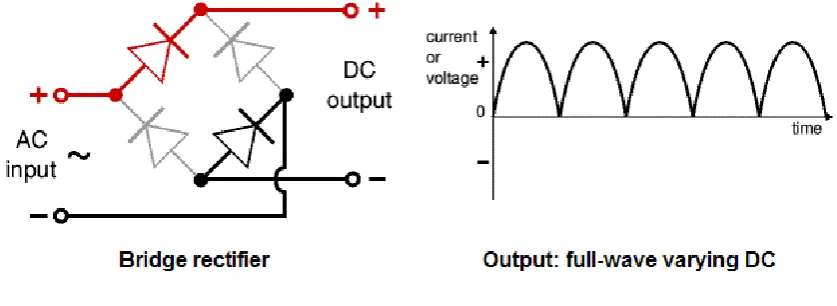
2.3 Single Phase Rectifier (Full-wave bridge rectifier)
Figure 2. 2: Full wave bridge rectifier.
2.4 Smoothing Circuit
[image:19.595.131.508.460.574.2]Smoothing circuit is used to smooth the DC from varying greatly to a small ripple. Smoothing is performed by a large value electrolytic connected across the DC supply to act as a reservoir, supplying current to the output when the varying DC voltage from the rectifier is falling.
Figure 2. 3: Capacitor charging and discharging
Figure 2.3 shows the unsmoothed varying DC (dotted line) and DC, and then discharges as it supplies current to the output.The smoothing significantly increases the average DC voltage to almost the peak value . The DC voltage can be calculated as follows:
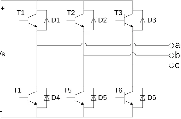
2.5 Three Phase Controlled Inverter
The main objective of static power converters is to produce an ac output waveform from a dc power supply. These are the types of waveforms required in adjustable speed drives (ASDs), uninterruptible power supplies (UPS), static var compensators, active filters, flexible ac transmission systems (FACTS), and voltage compensators, which are only a few applications [8].
T1
D1
T1
D4 T2
D2
T5
D5 T3
D3
T6
D6
Vs
b
c
a
+
-Figure 2. 4: Three phase transistor controlled inverter.
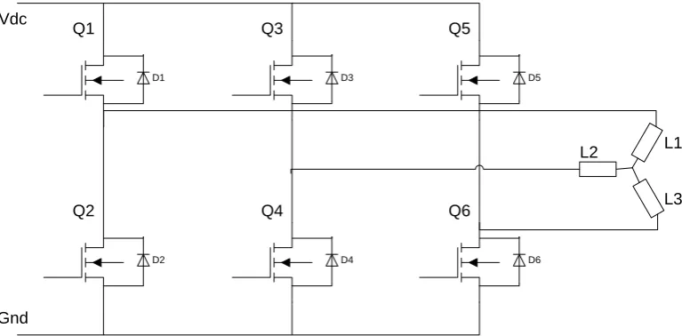
[image:20.595.164.457.253.446.2]Q1 D1 Q3 D3 Q5 D5 Q2 D2 Q4 D4 Q6 D6 L2 L3 L1 Vdc Gnd
Figure 2. 5: 6-pulse MOSFET controlled inverter.
For a high power application, MOSFET is used to replace the BJT as in Figure 2. 5. MOSFET does not depend on current triggers as BJT does. Therefore the MOSFET is fully triggered even with minutest current at its gate. Each of these MOSFET is triggered by PWM signal generated by the HB controller through gate driver circuit.
2.6 Three Phase Gate Driver
There are numerous IC gate drives that are commercially available for gating power converters. These include pulse-width modulation (PWM) control, power factor correction (PFC) control, combined PWM and PFC control, current mode control, bridge driver, servo driver, hall-bridge drivers, stepper motor driver and thyristor gate driver [8].
Recently, the interest with solid state pulsed power modulator has been growing because of many advantages such as long life span, rectangular pulse waveforms and easiness of controlling the pulse width and repetition rate [9]
suppress cross-talk and EMI noise, and also limit the power device stresses at switching transients. However, these conflicting requirements are difficult to be realized in a conventional gate driver [10].
Basically, the purpose of using a gate driver is the application of to charge pump circuit to the gate of the MOSFET in the rectifier circuit. The gate requirements for a MOSFET or an IGBT switch are satisfy as follows; i) Gate voltage must be 10V to 15V higher than the source or emitter voltage. Because the power drive is connected to the main high voltage rail +Vs, the gate voltage must be higher than the rail voltage. ii) The gate voltage that is normally referenced to ground must be controllable from the logic circuit. Thus, the control signals have to be level shifted to the source terminal of the power device, which in most applications swings between the two rails V+. iii) A low-side power device generally drives the high-side power device that is connected to the high voltage. Thus, there is one high-side and one low-side power device. The power absorbed by the gate drive circuitry should be low and it should not significantly affect the overall efficiency of the power converter [8].
2.7 Controller
Controller can be divided into two; adaptive and passive controller. PID, Fuzzy and Neural Network are in adaptive category while Hysteresis, Relay and Sliding Mode Control are in passive categories. All of this controller have their own disadvantage. For example, the disadvantage of sliding mode control method is chattering of the system states due to high control activity [11] .
2.7.1 Proportional-integral-derivative Control
( ∫
) (2.2)
Where Pout is the output from the controller when there is an error e which is
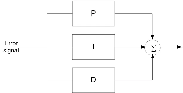
changing with time t, Vo is the set point output when there is no error, KP is the proportionality constant, KI the integral constant and KD the derivative constant. One way of considering a three controller is as a proportional controller which has integral control to eliminate the offset error and derivative control to reduce time lag [12].
P
I
D
[image:23.595.162.468.264.420.2]Error signal
Figure 2. 6: A PID controller
Figure 2. 6 show the block diagram of a PID controller. The error signal is the difference between reference/set point and the feedback.
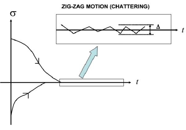
2.7.2 Sliding Mode Control
Sliding mode control (SMC) has been known for several decades and is still, due to its simplicity interest among application engineers and researchers [13]. SMC is known to be a robust control method appropriate for controlling uncertain systems. High robustness is maintained against various kinds of uncertainties such as external disturbances and measurement error. It is also straightforward to implement the resulting algorithms. Sliding mode control has long been considered for control of dynamic nonlinear systems. The need of SMC is to use a high speed switching control to move system’s state trajectories onto specified and user chosen surface in
the state space, known as the sliding surface or switching surface which keep the system’s state trajectory along the surface.
Figure 2. 7: State trajectory and sliding surface in SMC
Figure 2.7 shows the state trajectory and sliding surface in SMC. Once the state trajectory intercepts the sliding surface, it remains on the surface for all time and sliding along the surface, hence the term sliding mode. In the design of sliding mode controller the first stage is a design of sliding surface while the second is forces the state to approach the sliding surface from any other region of the state space, and remains on it [14].
Paper [14] purpose the design and implementation of sliding mode control for level control. The control problem is to find a suitable control input u(t)such that the output tracks a desired command asymptotically in the presence of model uncertainties and disturbances. The tracking error e(t), in terms of the command signal, yr(t) and measured output signal, ym(t), is defined as:
( ) ( ) ( ) (2.3)
State traject ory Sliding
The sliding surface s(t) which depend of tracking error e(t) and derivatives(s) of tracking error given as:
( ) (
)
( ) (2.4)
The n indicates the order of uncontrolled system, is the positive constant and the control input u(t) can be given as:
( ) ( ) ( ) (2.5)
[image:25.595.168.470.335.546.2]Where the ( ) is the equivalent control and ( ) is the switching control.
Figure 2. 8: Chattering on the output.
2.7.3 Hysteresis Band
[image:26.595.166.473.217.494.2]Hysteresis band controller is one of the passive controllers. The HB PWM technique is widely used because of its simplicity of implementation, and fast control [16]. Besides being simple, hysteresis controller provides higher tracking ability for the inverter [17].
Figure 2. 9: Hysteresis Band Controller [18]
The hysteresis modulation is a feedback current control method where the load current tracks the reference current within a hysteresis band. Figure 2.9 shows the operation principle of the hysteresis modulation.
Paper [19] purposed basic structure of a single phase current hysteresis control loop of a voltage source chopper while paper [20] HB pulse with modulated current controller applied to a three phase VSI inverter. It apply HB controller with the band of hysteresis maintained constant all the period of fundamental. The algorithm for the scheme is given as:
( ) (2.6)
Upper band: ( ) (2.7) Lower band: ( ) (2.8)
Where is the reference current, and is the upper and lower band current respectively while is the hysteresis band limit [19].
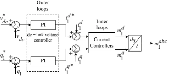
[image:27.595.185.459.420.544.2]2.8 Power transfer control of Back-to-back converter
Figure 2. 10: Control block diagram for VSC1
The control-block for BTB converters typically consist of two converters (VSC1 and VSC2). The control scheme for BTB converter shows in Figure 2. 10. The control blocks contain two blocks connected in cascade, called outer and inner loop. The inner loop is used to ensure an asymptotical tracking and the outer loop to control the DC-link for VSC1 [3].
inner loop for current control and outer loop for DC-link voltage and active/reactive power control as show in Figure 2.11.
[image:28.595.136.504.134.326.2]. Figure 2. 11: Complete BTB control structure.
Part of the control technique of VSC2 will be implemented in this project to control active/real power of the inverter. Y connected load is used in this system. For this type of load, the power consumed is given by:
(2.9)
The IL = I and VLL = √ , hence the power consumed by the three phase load can also be expressed as[21]:
√ (2.10)
2.9 MATLAB-Simulink Software
Simulink is a software package for creating, editing and simulating dynamical systems on MATLAB from Mathworks. It enables rapid construction of virtual prototypes to explore design concepts at any level of detail with minimal effort. For modelling, Simulink utilizes a graphical user interface (GUI) for building models where models are created as block diagram [22]. It includes a comprehensive library of predefined blocks to be used to construct graphical models of systems using drag-and-drop mouse operations.
User is able to produce an ―up-and-running‖ model that would otherwise require hours to build in the laboratory environment. It supports linear and nonlinear systems, modelled in continuous-time, sampled time, or hybrid of the two. Since students learn efficiently with frequent feedback, the interactive nature of Simulink encourages you to try things out, you can change parameters ―on the fly‖ and immediately see what happens, for ―what if‖ exploration. Lastly, and not the least, Simulink is integrated with MATLAB and data can be easily shared between the programs [23].
2.10 Raspberry Pi
Figure 2. 12: Raspberry Pi Type B; single-board credit-card size computer
Figure 2. 12 show the RPI type B. At the time of this project, there is a newly launched model of RPI known as type B+ with some enhancement on GPIO.
Table 2. 1: Comparison between Raspberry type B and B+
Technical Type B Type B+
Chip Broadcom BCM2835 SoC full HD multimedia applications processor
Broadcom BCM2835 SoC full HD multimedia applications processor
CPU 700 MHz Low Power
ARM1176JZ-F Applications Processor
700 MHz Low Power ARM1176JZ-F Applications Processor
GPU Dual Core VideoCore IV® Multimedia Co-Processor
Dual Core VideoCore IV® Multimedia Co-Processor
Memory 512MB SDRAM 512MB SDRAM
Ethernet onboard 10/100 Ethernet RJ45 jack
onboard 10/100 Ethernet RJ45 jack
USB 2.0 Dual USB Connector 4 x USB Connector Video output HDMI (rev 1.3 & 1.4)
Composite RCA (PAL and NTSC)
HDMI (rev 1.3 & 1.4) Composite RCA (PAL and NTSC)
Onboard storage SD, MMC, SDIO card slot Micro SD
Operating system Linux Linux
Table 2.1 shows the comparison between Raspberry Pi type B and B+. Raspberry Pi type B+ have nearly the same specification compared to type B. Type B+ has more GPIO’s and allow more devices to be connected. Type B will be utilize in this project since the Type B+ can only be used with MATLAB 2014a and above.
The Raspberry Pi will be utilized as a controller in this project. A control scheme will be develop using MATLAB-Simulink and download to Raspberry Pi. System MATLAB-Simulink plus Raspberry Pi have an advantage of real-time control and data acquisition compared to system with MATLAB-Simulink plus Arduino.
[image:31.595.106.533.377.494.2]Compared to Arduino Uno, the performance of RPI are much better in term of speed and connectivity. That is the main reason to choose this type of micro controller.
Table 2. 2: Comparison between Arduino Uno and Raspberry Pi
Specification Arduino Uno Raspberry Pi
Processor ATMega 328 ARM11
Clock speed 16Mhz 700Mhz
RAM 2KB 256MB
Ethernet Not available 10/100
GPU Not available Video Core IV
CHAPTER 3
METHODOLOGY
3.1 Introduction
These sections address the method on how this project carried out. All objective must be clearly stated in order to solve it with correct method. Figure 3.1 shows the project flowchart. At the first stage, the problem statement is defined with objectives and scopes of the project. Research on related field is then conducted together with review of previous research that has been made. This preliminary research will give an idea on method to solve the problem.
Start Project
Problem Statement, Objective, Scope
Study on related field, previous research
Simulation performance analysis
Hardware development Achieved?
Testing & Troubleshooting
Achieved?
Integrate Software & Hardware
Achieved? Testing & Troubleshooting
Report & Presentation
[image:33.595.150.463.53.729.2]End Project
3.2 Specific Block Diagram of Project INVERTER Vs RECTIFIER i S E N S O R v S E N S O R MATLAB Simulink GATE DRIVER RASPBERRY PI Hyteresis Band PIC
Figure 3.2: Specific Block Diagram of Project
In Figure 3.2, there are two section of this project; software development and hardware development. Hardware development consists of circuit construction for controlled rectifier, inverter, and gate driver circuit. While software development consists of Hysteresis Band controller using MATLAB-Simulink interfaced with Raspberry Pi.
3.3 Software Development
There are two main sections in software development; development of Hysteresis Band controller and interfacing with Raspberry Pi using support package provided.
3.3.1 Proposed control strategies
Raspberry Pi and PIC
HB in
MATLAB-Simulink Inverter Load
Current (RMS) +
-Voltage (RMS) Power
(reference) Divide
Iref
[image:35.595.66.562.224.364.2]Iline
Figure 3. 3: Closed-loop of power transfer control system.
Control scheme employed to control the power transfer to the load are shown in Figure 3.3. The objective is to control power transfer to motor according to reference value. The power (reference) will divide with RMS voltage to obtain the current value. This current value will be the set point or Iref to the current controller. A passive controller known as Hysteresis Band controller, embed in MATLAB-Simulink to manipulate the parameters from current sensors and voltage sensor. It is known that these two parameters contribute to Power as following equation:
(3.1)
3.3.2 Hysteresis Band Controller Development
The software development which consist of Hysteresis Band controller using MATLAB-Simulink software. Figure 3.4 shows the block diagram of HB controller that will be developed using MATLAB-Simulink function block. The technique used in control scheme is using current control where Ia is the feedback current from current sensor while Iref is the reference current or set point for the system.
Hysteresis Band Controller
Iref +
-Ia
[image:36.595.165.488.231.324.2]To Gate Driver
Figure 3. 4: Hysteresis Band controller.
As a basic design of HB controller, the HB must contain reference current, upper band and lower band of HB controller. As in Figure 2. 8. The error (e) is the difference between output current and reference current and can be written as below:
(3.3)
Where is the output current and is the reference current. In HB controller, the output voltage level depends on the error between the current set point and the real current injected by the inverter. To set the upper and lower band, the following equation is used:
(3.4)
REFERENCES
[1] Theodore Wildi, Electrical Machines, Drives, And Power Systems, 6th ed. Ohio: Pearson Prentice Hall, 2006.
[2] Vandyk Amsdem Fernandes and Junieta Sequeira Viren Pereira, "Low Cost Object Sorting Robotic Arm using Raspberry Pi ," in IEEE Global
Humanitarian Technology Conference - South Asia Satellite (GHTC-SAS), Shiroda - Goa - India, 2014, pp. 1 - 6.
[3] Ernesto Barcenas, Victor Cardenas Janeth Alcala, "Practical Method for tuning PI controllers in the DC-linl Voltage Loop in Back-to-back Power Converters," , 2010, pp. 46-52.
[4] V. Cardenas, J. Alcala, C.Nunez E.Rosas, "Active and REactive Current Control Strategy Applied to a SIngle-Phase BTB Converter,".
[5] Md Zarafi Ahmad, Farrah Salwani Abdullah Afarulrazi Abu Bakar, "Design of FPGA - Based SPWM Single Phase Full-Bridge Inverter".
[6] Huajie Yin, Lian Guan Wanwei Wang, "Study on Back-to-back PWM Converter Based on Direct Power Control for Induction Motor Drive,". [7] Chung-Chuan Hou, "A Common Single-Phase Diode Rectifier forMulti-Load
System with an Auxiliary Converter," in The 2010 International Power Electronics Conference, Taiwan, 2010, pp. 1586 - 1589.
[8] Muhammad H. Rashid, Power Electronics Handbook.: Academic Press, 2001. [9] S.R. Jang and S.H. Ahn, "A Comparative Study of the Gate Driver Circuits for
Series Stacking of Semiconductor Switches," , 2010, pp. 326-330. [10] X. Shi, L.M Tolbert, and B.J. Blalock Z. Wang, "Switching Performance
Improvement of IGBT Modules Using an Active Gate Driver," , 2013, pp. 1226-1273.
[12] W Bolton, Inudstrial Control & Instrumentation. Burnt Mill, Harlow, England: Longman Scientific & Technical, 1991.
[13] Asifˇ Sabanovic, "Variable Structure Systems With Sliding Modes in Motion Control—A Survey," in IEEE TRANSACTIONS ON INDUSTRIAL
INFORMATICS, 2011, pp. 212 - 223.
[14] Jadhav V. K., Lokhande N. N. Parvat B. J., "Design and Implementation of Sliding Mode Controller for Level Control," IOSR Journal of Electronics and Communication Engineering (IOSR-JECE), pp. 51 - 54.
[15] Kanungo Barada Mohanty, "Sensorless Sliding Mode Control of Induction Motor Drives," Electrical Engineering Department, National Institute of Technology, Rourkela,.
[16] BIMAL K. BOSE, "An Adaptive Hy steresis-Band Current Control Technique of a Voltage-Fed PWM Inverterfor Machine Drive System," IEEE
TRANSACTIONS ON INDUSTRIAL ELECTRONICS, vol. 37, pp. 402 - 408, October 1990.
[17] M.H. Kordi, G. Griva, and A. Tenconi S.M.R. Rafiei, "Nash Genetic Algorithm Based Optimal Design of Hysteresis Inverters for Active Power Filtering Applications," in IEEE Bucharest Power Tech Conference, Romania, 2009, pp. 1 - 5.
[18] Matlab. (2014) www.matworks.com. [Online].
http://www.mathworks.com/help/physmod/sps/powersys/ug/simulating-an-ac-motor-drive.html
[19] and A. Moussi K. Derradji Belloum, "A Fixed Band Hysteresis Current Controller for Voltage Source AC Chopper ," International Journal of
Electrical, Computer, Electronics and Communication Engineering, vol. 2, no. 9, pp. 127 - 133, 2008.
[21] Stephen J. Chapman, Electric Machinery and Power System, International ed. Australia: McGraw Hill, 2002.
[22] George Rost, C.O. Nwankpa Anawach Sangswang, "A Modular Simulink-Based Controlled Three- Phase Switch Mode Inverter," in IEEE, Pennsylvania, 2000, pp. 2101 - 2106.
[23] IEEE. Chapter 8 - Simulink Tutorial.
[24] Bhanuprasad Patibandala, Harish Santhanam, Sindhura Gaddam, Vamsi Krishna Alla, Gopinath Shanmuga Sundaram, "Bluetooth Communication using a
Touchscreen Interface with the Raspberry Pi ," , Charlotte, USA, 2013. [25] Sławomir Michalak, "Raspberry Pi as a Measurement System Control Unit,"
Poznan University of Technology , Poznań, Poland, 2014. [26] Raspberry Pi Foundation. raspberry pi. [Online].
http://www.raspberrypi.org/help/what-is-a-raspberry-pi/
[27] Rosni Abu Kassim and Norlida Buniyamin Md Saifudaullah Bin Bahrudin, "Development of Fire Alarm System using Raspberry Pi and Arduino Uno ," in
2013 International Conference on Electrical, Electronics and System
Engineering , 2013, pp. 43 - 48.
![Figure 2. 1: Back-to-back power topology [3]](https://thumb-us.123doks.com/thumbv2/123dok_us/8762463.894657/17.595.120.518.582.692/figure-back-to-back-power-topology.webp)

![Figure 2. 9: Hysteresis Band Controller [18]](https://thumb-us.123doks.com/thumbv2/123dok_us/8762463.894657/26.595.166.473.217.494/figure-hysteresis-band-controller.webp)