
i
THE EFFECTS OF DESIGN AND
ENVIRONMENTAL FACTORS ON THE
RELIABILITY OF ELECTRONIC PRODUCTS
Wayne Lawson
B.Eng.(Hon)., M.Sc., C.Eng.
The Effects of Design and Environmental Factors on
the Reliability of Electronic Products
Wayne LAWSON
B.Eng., M.Sc., C.Eng.
Materials Research Institute (MRI)
School of Computing, Science and Engineering
University of Salford, Salford, UK
i
TABLE OF CONTENT
TERMS OF REFERENCE ACKNOWLEDGEMENTS LIST OF FIGURES
LIST OF TABLES ABSTRACT
CHAPTER ONE: INTRODUCTION ... 1
1.1ELECTROCHEMICAL DEGRADATION OF PRINTED CIRCUIT BOARDS ... 1
1.2ELECTROCHEMICAL MIGRATION (ECM) ... 2
1.3AIMS AND OBJECTIVES ... 5
1.4THESIS OUTLINE ... 7
CHAPTER TWO: BACKGROUND AND LITERATURE REVIEW ... 8
2.1MATERIALS USED IN THE ELECTRONICS INDUSTRY ... 10
2.1.1 Printed Circuit Boards ... 10
2.1.2 Metals ... 13
2.1.3 Flux ... 14
2.2ELECTROCHEMICAL MIGRATION ... 16
2.2.1 Anode and Cathode ... 18
2.2.2 Electrolysis of Water ... 19
2.2.3 Pourbaix Diagrams ... 25
2.2.4 Metal Migration Potential on Electronic Products ... 26
2.3ELECTROCHEMICAL FAILURES ON ELECTRONIC PRODUCTS ... 30
2.3.2 Conductive Anodic Filaments (CAFs) ... 37
2.3.3 AC Formations ... 40
2.4METHODS FOR DETECTING IONIC MIGRATION ... 46
2.4.1 Surface Insulations Resistance (SIR) ... 47
2.4.2 A Novel Method for Analysing CAFs ... 52
2.4.3 Saturated Condition Test ... 53
2.5ACCELERATED LIFE TESTING OF ELECTRONIC PRODUCTS ... 54
2.6PREVENTATIVE MEASURES AND DENDRITE DESIGN CONTINGENCY... 56
CHAPTER THREE: EXPERIMENTAL APPROACH ... 59
3.1SAMPLE DESIGNS ... 59
3.1.1 Removing the Gold Plating ... 61
3.1.2 Sample Preparation ... 63
3.2DESIGN OF EXPERIMENT ... 64
3.3EXPERIMENT STRUCTURE –FLOWCHART ... 66
3.4EXPERIMENTAL SETUP ... 67
3.5FUNDAMENTAL EXPERIMENT –OBSERVATIONS OF DENDRITES ... 67
3.5.1 Configuration of Experiment 1A: Metal Dissolution in Water ... 68
3.5.2 Configuration of Experiment 1B: Demonstrating pH Changes at Electrodes ... 69
3.5.3 Configuration of Experiment 1C: Parameters for Dendrite Growth ... 70
3.5.4 Configuration of Experiment 2 – Dendrite Growth in Saturated Conditions ... 73
CHAPTER FOUR: FUNDAMENTAL EXPERIMENTAL OBSERVATIONS OF DENDRITES... .... 75
CHAPTER FIVE: RESULTS AND DISCUSSIONS OF EXPERIMENT 1 – PARAMETER SPACE OF DENDRITIC GROWTH ... 81
5.1EXPERIMENT 1A:METAL DISSOLUTION IN WATER ... 81
5.1.2 Discussion ... 84
5.2EXPERIMENT 1B: PHCHANGES AT THE ELECTRODE INTERFACES ... 86
5.2.1 Discussion ... 89
5.3EXPERIMENT 1C:PARAMETERS FOR DENDRITE GROWTH ... 90
5.3.1 Potential Sweep ... 92
5.3.2 Discussion ... 98
5.4EXPERIMENT 1D–ANALYSIS OF DENDRITE FILAMENTS ... 99
5.4.1 Discussion ... 103
5.5CONCLUSION ... 104
CHAPTER SIX: RESULTS AND DISCUSSIONS OF EXPERIMENT 2 – DENDRITE GROWTH IN SATURATED CONDITIONS ... 106
6.1MODELING GROWTH OF COPPER DENDRITES IN SATURATED CONDITIONS ... 106
6.2DISCUSSION OF RESULTS ... 109
6.2.1 Model of Dendrite Initiation Time ... 113
6.3SUMMARY ... 116
CHAPTER SEVEN: CONCLUSIONS AND SUGGESTIONS FOR FURTHER WORK .... 117
7.1CONCLUSIONS ... 117
7.2DESIGN GUIDELINES ... 120
REFERENCES
APPENDIX 1: PUBLICATIONS
a) Published Paper, Lawson, W and Pilkington, RD and Hill, AE, 2007, 'Modeling and analysis of the growth of copper dendrites in saturated conditions using a multilevel factorial design analysis' , Microelectronics International, 24 (2) , pp. 28-34.
b) Internal White Paper: Lawson, W, Brief Introduction to Dendrites and CAFs on Printed Circuit Boards, Delphi Electronics Group, August 2007.
ACKNOWLEDGEMENTS
This research could never have been completed if it had not been for the support of my family, especially for Catherine’s compassion and patience in light of our recent addition, Amelia.
I am indebted to my project supervisor, Dr Richard Pilkington, who provided vital support and help through his encouragement and compassion.
I would like to give my sincere thanks to Delphi for funding this PhD and the support over my years of study. I would especially like to thank John McColl, who now has left Delphi, for providing the opportunity to pursuit this line of study. Not forgetting, Bob Schofield and Ian Gaskell for continuing this support. Even more so to Bob for his steady guidance and the use of his red pens!
ABSTRACT
The reliability of electronic products is fast becoming of major importance with the demand for increased safety, especially in the automotive industry. Tracks, pads and vias on printed circuit boards can suffer a variety of problems if circuits are contaminated with electrical-conducting substances.
Electrochemical migration, especially dendrite growth, has long been a concern in safety critical and durable systems, and current preventative methods tend to focus on various styles of printed circuit board protective coatings. These measures have a number of disadvantages, mainly process and material costs with extreme scepticism on their overall efficacy. Any design related developments that can minimise the impact of dendrite growth on reliability can lead to a more economic, durable and safer product.
The work in this thesis provides a thorough literature search of the field of electrochemical migration on printed circuit boards. This study then develops a novel circuit-design-orientated model, based on a multilevel full-factorial design, to study the effects of temperature, voltage and electrode gap on dendritic growth under saturated conditions. Preparation of several DC-biased copper-comb patterned printed circuit boards placed in temperature-controlled water-filled cuvettes enables the specific monitoring of dendrite activity, and detects a sharp current increase that accompanies a dendritic short circuit condition.
A high R2 polynomial correlation-model is derived and it is noted that increased voltage and temperature and reduced track spacing increases the impact of dendritic growth on reliability. At voltages between 3 and 4V, gas bubble formation at the electrodes has the effect of increasing reliability by destroying the dendrite fuses. It is shown that dendrites may not grow below 1.25V, which coincides with the theoretical onset voltage for the decomposition of water. It was also demonstrated that electrically biased, water-contaminated printed circuit boards form extreme acid and alkaline regions close to the anode and cathode terminations, respectively, which can cause corrosion.
GLOSSARY
Adsorption: The take-up of a substance at the surface of another material
Anode and cathode: Anode and cathode are the positive and negative polarities of an electrochemical system, respectively.
CAF: Conductive Anodic Filaments are electrochemical growths between the laminates of printed circuit boards, which are usually formed from copper.
Copper-clad: Printed circuit board before the etching process. This is usually thin copper bonded to a fibre glass substrate.
Corrosion: The decomposition of a metal due to the exchange of electron and the formation of ionic species usually in an aqueous solution.
Dendrite: Electrochemical growths with a fractal-like structure
Dendrite fusing: The point when a dendrite shorts between two electrically biased electrodes causing a reduction in resistance.
Double-layer capacitance: A capacitance created by the charge of molecules between metal-liquid interfaces below the overvoltage potential.
EDX: Energy-dispersive X-ray spectroscopy, used to analyse the atomic composition of a material.
Factors: A parameter under consideration that can influence the response variable
Flux: A liquid substance use to clean metallic surface before a solder wets
Halide: The ionised form of halogens
Halogens : A series of non-metal elements from the periodic table, comprising fluorine, chlorine, bromine, iodine, and astatine.
Hydroscopic : A material’s ability to absorb moisture from the atmosphere
Hydroxide: The ion form of OH
Interaction: Two or more variables that interact with each other and hence the response
Migration: The movement of ions through an electrolyte
Nernst diffusion-layer: A linear diffusion region adjacent to an electrode where the species concentration remains stagnant and is unchanged by time when electrolysis occurs.
Noble metal: Metal that is more resistant to corrosion or oxidation.
Overvoltage: The additional potential added to the theoretical activation energy required for electrolysis to occur.
Pad: The metallic area of a printed circuit board where electronic component leads are soldered
PCB: Printed Circuit Board
Pourbaix Diagram: A diagram used to plot electrochemical reaction relative to potential and pH, named after it creator Marcel Pourbaix (1904-1998), also known as Potential-pH diagram.
p-value: The probability of the event happening.
Redox: Reduction and Oxidation
Reflow soldering: A method of forming a solder joint between component and circuit board by heating solder paste to its alloy liquidus temperature
Regression: A method of determining the next response from historical data.
RH Relative Humidity (scale 0-100%)
RMA Flux activation level. Rosin Mildly Activated.
Rosin: A natural product from the sap of pine trees and the main ingredient in solder fluxes.
R-square: The difference between the observed data and the model. A high percentage value indicates that the model closely represents the observed data.
SEM: Scanning Electron Microscope used for producing high-resolution images
SHE Standard Hydrogen Electrode
SIR: Surface Insulation Resistance
LIST OF FIGURES
Figure 1 – Cross-section of a PCB Via Showing Evidence of CAF ... 3
Figure 2 – Example of a Dendrite ... 4
Figure 3 – Two Types of Electrochemical Migration ... 8
Figure 4 – Formations of tin/lead Dendrites on a SMD Capacitor (Delphi, 2005) ... 9
Figure 5 – Example of a Dendrite between Two Copper Tracks ... 9
Figure 6 – Cross-section of a Multilayer Board ... 11
Figure 7 – SEM of FR4 substrate ... 12
Figure 8 – EDX of FR4 Image ... 13
Figure 9 – Effect of Temperature on SIR at 85% RH[38] ... 15
Figure 10 – A Typical Surface Mount Process Flow ... 16
Figure 11 – Copper Migration of PCB Tracks ... 17
Figure 12 – International Convention of Electrode Polarity ... 18
Figure 13 – A Typical Aqueous Electrochemical Cell ... 19
Figure 14 – Demonstration of pH Gradients at the Metal Interfaces ... 20
Figure 15 – Charging of the Double-Layer within Decomposition Voltage ... 24
Figure 16 – Outline of a Pourbaix Diagram for an Aqueous Systems [50] ... 25
Figure 17 – Copper Pourbaix Diagram at 25°C[60] ... 26
Figure 19 – Pourbaix Diagrams of Metals that Migrate with Deionised Water[50] ... 28
Figure 20 – Pourbaix Diagrams of Metals that may need other Conditions to Migrate[50] 29 Figure 21 – 9K x Magnification of a Dendrite Showing Fractal-like Branching ... 31
Figure 22 – Large Current Density at the Tip of a Nucleus ... 31
Figure 23 – Basic Mechanism of Dendrite Formation ... 32
Figure 24 – Dendrite Shapes as a Function of Concentration Gradient[66] ... 33
Figure 25 – Overview of Electrochemical Migration [49] ... 35
Figure 26 – Micro-steps [72]... 35
Figure 27 – Representation of a Concentrated Electrical Field [71] ... 36
Figure 28 – The Nernst Diffusion-layer Thickness (δ) ... 37
Figure 29 – Schematic of a CAF Pathway between Two Vias ... 38
Figure 30 – Simplified Copper Pourbaix Diagram 25ºC [50] ... 39
Figure 31 – AC Bias Cell: Idealised Relationship of a Copper Ion Migration path ... 41
Figure 32 – AC Dendrite Growth (a: 0.001Hz, b: 0.1Hz) ... 42
Figure 33 – Diffuse, White or Blue-green Residue on AC Circuits ... 43
Figure 34 – Venn Diagram of Electrochemical Failure Modes ... 47
Figure 35 – IPC-B-25A Test Comb[89] ... 48
Figure 36 – Current and SIR for Coupon Contaminated with Salt Solution 10µg/in2[84] .. 50
Figure 37 – Dendrites Fusing in Commercial Water ... 51
Figure 38 – Electrical Schematic of Ready’s Linear Circuit[22] ... 53
Figure 40 – Image of Vero Board Used ... 59
Figure 41 – Left, PCB Design. Right, Magnified View of SMD Sample ... 60
Figure 42 – Top, Single Comb Sample. Bottom, 0.4 mm spaced SMD Sample ... 61
Figure 43 – After Gold has been Removed ... 61
Figure 44 – EDX after Gold Removal, Note the high iodine content. ... 62
Figure 45 – EDX of Ammonia Cleaned Comb, Note the absence of iodine. ... 63
Figure 46 – Experiment Flow Chart ... 66
Figure 47 – Setup of Biased Piece of Vero Board ... 67
Figure 48 – Equipment Configuration for Metal Leaf Test ... 68
Figure 49 – Custom Electrochemical Cell ... 69
Figure 50 – Printed Circuit Board pH Sample ... 70
Figure 51 – Schematic of Conditional Dendrite Growth Equipment ... 71
Figure 52 – Photograph of Conditional Controlled Dendrite Growth Equipment ... 72
Figure 53 – Water Filled Cuvette Test ... 73
Figure 54 – Schematic: Dendrite Growth under Saturated Condition Equipment... 74
Figure 55 – DC bias on copper initial state ... 75
Figure 56 – DC bias on copper just after bias applied ... 76
Figure 57 – First Phase of the Growth of Dendrites ... 77
Figure 58 – A Dendrite Dominates the Current Path. ... 77
Figure 59 – Moment the Dendrite made Contact with the Anode, before it ‘fused’. ... 78
Figure 61 – Final Stages of Experiment: Blue-crystallised Finish ... 79
Figure 62 – Copper Dissolution in Water at the Anode: Cu+Cu Electrodes ... 82
Figure 63 – Dendrites Forming at Platinum Electrode ... 83
Figure 64 – Electrolysis with Copper Cathode and Platinum Anode ... 84
Figure 65 – pH Change in vicinity of Electrodes ... 86
Figure 66 – Demonstration of pH at both Anode and Cathode... 87
Figure 67 – High pH Gradient on Two Pads of Printed Circuit Board ... 88
Figure 68 – Voltage Level Observations at 30°C ... 91
Figure 69 – Voltage Sweep from 0V to 4V over 400 Seconds ... 92
Figure 70 – Voltage and Temperature Effect on Migration, Current in linear [top] and log scales [bottom] ... 93
Figure 71 – At 30°C Sweep captured at 2.8V ... 95
Figure 72 – At 30°C Sweep captured at 3.25V ... 95
Figure 73 – At 35°C Sweep captured at 2.5V ... 96
Figure 74 – At 35°C Sweep captured at 3.55V ... 96
Figure 75 – At 40°C Sweep captured at 2.45V ... 97
Figure 76 – At 40°C Sweep captured at 2.8V ... 97
Figure 77 – 50x Magnification of a Comb with Dendrite ... 100
Figure 78 – 200x Magnification of the Dendrite Shown in Figure 77 ... 101
Figure 79 – 200x Magnification of a Dendrite Branching Toward 2nd Cathode ... 101
Figure 81 – 7Kx Magnification of a Dense Dendrite Tip ... 102
Figure 82 – EDX Analysis of Dense Dendrite Tip in Figure 81 ... 103
Figure 83 – 1.2ml Cuvette ... 106
Figure 84 – Copper Interdigitated Printed Circuit Boards ... 107
Figure 85 – Example i-t Plot for 5.25v and 1.25v at 25°C and Gap Spacing on 0.2 mm .. 108
Figure 86 – Pareto of Response D_init_time_sec ... 112
Figure 87 – D_init_time_sec as a Function of Voltage and Temperature, with Gap held at 0.3 mm. ... 114
Figure 88 – D_init_time_sec as a Function of Voltage and Gap, with Temperature held at 25°C. ... 115
Figure 89 – D_init_time_sec as a Function of Temperature and Gap, with Voltage held at 3.25V. ... 115
Figure 90 – Summarised Pourbiax Diagram for Copper ... 118
Figure 91 – Quick Reference Design Guideline for Reducing Dendrite Growth ... 120
Figure 92 – Effect of Track Spacing on Dendrite Growth ... 121
Figure 93 – Effect of Temperature on Dendrite Growth... 122
LIST OF TABLES
Table 1 – Typical Composition of Rosin[14, 36, 37] ... 14
Table 2 – Electrochemical Series of Metals Used in the Electronics Industry[52] ... 22
Table 3 – Average Overvoltage of Hydrogen on Various Metal Cathodes[54, 56] ... 23
Table 4 – ECM Condition for Different Metals Used in Electronics [61] ... 27
Table 5 – ΔG [52, 53] and calculated Ea values of Typical Ionic Species when Copper is Electrolysed in Water ... 30
Table 6 – Summary of SIR Standards and Some Parameters ... 46
Table 7 – Factors that can Influence Electrochemical Migration ... 46
Table 8 – Reaction at Both Electrodes ... 80
Table 9 – Summary of Dendrite Thresholds ... 90
Table 10 – Evaluation of the Preece Equation ... 94
Table 11 – Factors Included in Design of Experiments ... 108
Table 12 – ΔG [52, 53, 53] and Calculated Ea Values of Typical Ionic Species, when copper is electrolysed in water. ... 109
Table 13 – Multifactoral Runs and Experiment Results of D_init_time_sec, sorted by temperature. ... 111
Table 14 – ANOVA Table of Responses D_init_time_sec ... 113
Table 15 – Regression Coefficients Values from D_init_time_sec ... 113
1
Chapter One:
Introduction
Satellite failures are rare and very costly when they occur, with interconnection failures accounting for over 15% of satellite malfunctions[1]. In May 1998 a Boeing 601 telecommunications satellite, Galaxy 4, failed with drastic results[2]. The failure, which disabled telephone networks across the United States, was unexplained for many years although the failure mechanism was later believed to be the formation of tin growths. The earliest account of metal migration was a report on a telephone-switchboard by Kohman in 1955[3] who found an electrical field and water were needed for migration to occur through an electrochemical process.
Reliability of electronics is of paramount importance and failures can cause serious, if not disastrous, consequences. In the manufacture of electronic goods the drive towards longer field life and increased reliability is an ongoing trend, driven by a demand for improved reliability, durability and safety.
In the manufacture and assembly of printed circuit boards (PCB), residues produced by the process can be deposited on a PCB. When PCBs are energised by electronic signals, these residues can produce parasitic growths, potentially causing short circuits and the failure of the PCB. The occurrences of electrochemical migration failure modes, such as dendrites and conductive anodic filaments (CAF), are problems which can bring catastrophic failure and lead to the malfunction of mission critical systems[4].
1.1
Electrochemical Degradation of Printed Circuit Boards
Electronic equipment used under very dry conditions may not have such problems, unless there are large temperature fluctuations that result in dew condensation occurring on the surface of the circuitry or if the contaminants are hygroscopic and adsorb enough moisture to provide a liquid film on the surface. With high relative humidity conditions, a thin layer of moisture can occur on the surface which may be sufficient to decrease surface insulation resistance, cause corrosion or form metallic dendrites. Higher humidity can cause a thicker moisture layer and a faster corrosion or dendrite growth can then take place[5].
The problem of electrochemical degradation in electronic systems has long been recognized. The first dendritic failure was reported in 1955[3, 6], with further publications later[7-10]. CAF failure modes were first reported by Bell Laboratories in 1976[11].
More recently there has been an increase in reliability concerns arising from electrochemical degradation for three main reasons:
• Increased use of electronics in safety critical applications in harsh environments, such as in automotive, aviation and medical fields.
• Integration and the trend towards smaller multi-layer printed circuit board geometries.
• Increased use of lower operating currents and voltages (dendrite bridges will often self-heal if the current is large enough to blow the short).
1.2
Electrochemical Migration (ECM)
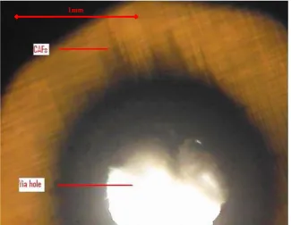
There are two distinct electrochemical migration failure phenomena that can occur on printed circuit boards. The first form is conductive anodic filament (CAF) formations. CAF failures in printed circuit boards occur under conditions of high humidity and high voltage gradients, with the filament composed of copper salts that grow from the anode towards the cathode along the fibres of the epoxy/glass interface. As CAFs are formed within the fibres it is not possible to see the failures on the surface of the substrate, as in the case of a dendrite, and substrate sectioning and polishing is required to expose the growth. An example section of a CAF is shown in Figure 1. Note the black CAFs spikes from the positive terminal, anode, emanating towards the ground plane, cathode.
Figure 1 – Cross-section of a PCB Via Showing Evidence of CAF
The second form of electrochemical migration failures and the focus of this thesis are surface dendrites. Dendrites can grow from the cathode to the anode under an applied voltage bias when aqueous contamination is present. These dendrites are fractal in shape, as in Figure 2, and can bridge the conductors (cathode-anode).
Figure 2 – Example of a Dendrite
In the presence of low currents (μA) dendrite shorts can be maintained. However, if the currents are sufficiently high they can blow, similar to a fuse. Dendrites differ from CAFs for a number of reasons as follows[13]:
• Dendrite growth usually occurs on the surface of a substrate/contact and not internally as in CAF growth.
• A dendrite can be formed from various metals such as copper, lead or tin, whereas in CAF growth, the migrating metal is usually copper.
• The direction of a dendrite’s filament growth is from the cathode to anode and not from the anode to the cathode as observed in CAF growth.
• The composition of a dendrite filament is understood to be neutral metal and not a metallic salt as found in CAF growth.
A full description of these aspects is given in Chapter 2.
1.3
Aims and Objectives
To better understand the problem contacts were established with Delphi Automotive Systems, The Test Lab (USA), National Physics Laboratories (NPL - UK) and Heraeus Circuit Materials (USA).
From discussions with these links, the broad aims and objectives of this research were established. The sponsoring company, Delphi Electronics Systems, has a particular interest in the following areas:
• Operating temperatures for automotive electronic engine controllers are extreme from -40ºC to 125ºC. However, whilst most of the validation for controllers operate at either end of these extremes the mechanisms of failures such as dendrites at normal ambient temperatures (5-50ºC) is assumed to be similar. Gaining an understanding of the operating parameters of typical failure mechanisms, such as dendrites, would benefit overall automotive electronic controller reliability.
• Further understanding of dendrite growth relative to the design parameters required to minimise or even eliminate their formation.
• Designing and developing a system to conduct analysis of typical ionic and dendritic formations on PCBs, whilst eliminating external factors that hinder experiments of parametric identification.
• Understanding mechanisms of dendritic growth under DC and AC conditions. Based on these requirements this research project investigates factors that enhance dendrite formation between printed circuit board (PCB) tracks. The main parameters studied are (1) conductor track spacing, (2) temperature, (3) operating voltage and (4) effect of pH.
The motivation for this research is to determine improved methods for assessing printed circuit board (PCB) reliability of current surface insulation resistance (SIR) failures. The author bases part of this study on his M.Sc – ‘Investigation into a modified area-of-spread method to monitor the effect of oxygen levels in a reflow oven’[14, 15] and, to a degree, on his B.Eng project ‘The effects of hydrogen/nitrogen mixtures on Soldering in Electronics of copper and tin/lead surfaces for PCB assemblies’[16].
1.4
Thesis Outline
This thesis is divided into seven Chapters and three appendices. Chapter 1covers the project background and the problem description. It also reviews the research objectives and gives an overview of the thesis. Chapter 2 presents the background and literature review on electrochemical failures. The first part of this Chapter outlines materials used in the electronics industry and then develops an understanding of electrochemical migration before moving on to mechanisms associated with electrochemical failures. Chapter 3 explains the methods and equipment used for the experiment outlined in Chapters 4 and 5. Chapter 4 presents the initial work on dendrite growth that forms the basic understanding for experimental methods used in Chapter 5. Chapter 5 is devoted to understanding the parameters that augment the growth of dendrites, which aids the development of a factorial design used in Chapter 6. Chapter 6 presents a multilevel factorial experiment as the basis for modelling three main parameter, temperature, voltage and track spacing. Chapter 7, the final Chapter presents the conclusion of the thesis and proposes areas for further investigation.
Chapter Two:
Background and Literature Review
Much work has been conducted on the reliability impact of metallic and slat deposits formed by an electrochemical process when a printed circuit board is contaminated with an aqueous solution[3, 17-23]. The earliest citation on electrochemical migration on printed circuit boards was published by Bell Systems[7], with most of the relevant subsequent publications, up to 1977, focussing on silver migration[7-9, 24].
Figure 3 – Two Types of Electrochemical Migration Dendrites and CAF
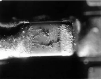
Figure 4 – Formations of tin/lead Dendrites on a SMD Capacitor (Delphi, 2005)
Figure 5 show the growth of a dendrite between two copper tracks.
To understand the nature of the electrochemical failure mode of electronic products it is important to review the construction of printed circuit boards, the metals used in the industry, flux and its removal, and electrochemistry.
2.1
Materials Used in the Electronics Industry
2.1.1
Printed Circuit Boards
Printed circuit boards (PCB) or printed wiring boards (PWB) were commercially introduced after World War II, usually credited to Paul Eisler[25, 26], and were primarily used for airborne instruments and for telecommunications. However, the substantial production of printed circuit boards did not start until the 1950s. Since its introduction, the printed circuit board has been used in most applications from communication satellites to the humble transistor radio.
The printed circuit board is constructed of conductors, also called tracks, consisting of copper strips adhered to an insulating substrate. There are four major printed circuit board constructs:
1) Single-sided boards: The copper is only present on one side of the insulating material.
2) Double-sided boards: The copper is present on both side of the insulating material and connections between the two sides are usually made by plated tin-lead alloy, commonly known as plated through hole (PTH) or vias.
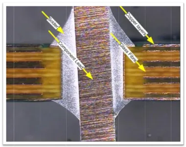
3) Multilayer boards: The copper is present on both sides of the insulating material with additional conductor layers inside the boards. Typical constructs are of four, six and eight layers, with the outer layer (top and bottom) used for power i.e. ground and other voltage levels. Figure 6 shows a cross-section of an eight-layer board with a component lead soldered at both ends of the board to a through-hole via.
The two o the solder and comp a single su The printe removing typically 3 chloride, a The insula Associatio • FR • FR
outer sides ( side and co onent side e urface. ed circuit b
unwanted 35μm and 7 ammonium
[image:28.595.133.514.99.400.2]ating mater on) grade. C R-2, FR3 – p R-4, FR-5, G
Figure 6 – C
(top and bot omponent si exist on bot
oard pattern copper fr 70μm[26]. persulphate rial is indic Commonly phenolic pap G-10, G-11
Cross-sectio
ttom) of the ide. Using th sides i.e.
ns are usua rom a cop Common c e, sodium pe ated by the
used substr per laminat – epoxy gla
on of a Mult
e printed cir surface mo componen ally formed pper-clad su chemicals u ersulphate a e NEMA (N rates are[26] te, used mos ass fibre rei
ilayer Board
rcuit board a ounted comp ts and solde
by a select ubstrate, w used for cop
and acid cup National Ele
]:
stly for sing inforced lam
d
are typically ponents the ering can be
tive etching with copper
pper etchin pric chlorid ectrical Ma
gle sided PC minate, used
y known as solder side e placed on
g process of r thickness g are ferric de.
anufacturers
CBs. d mostly for
Most of t flame-reta reports on virtually n shows a S substrate u Figure 7, d
these substr ardant. Wh
n the impac no effect o SEM of the used in auto demonstrati
Figu
rates contai hilst halide ct of brom on migration
e FR4 subst omotive ass ing the brom
ure 7 – SEM
in additiona e ions can mide on prin
n potential trate used i semblies. F mine peaks.
of FR4 sub
al compoun act as cata nted circuit
on FR-4 c in the exper Figure 8 sho
strate
nds, namely alysts in lo t boards de circuit boar
riments for ows an EDX
y bromide, ocalised co emonstrate rds[28, 29].
this thesis X of the FR
Figure 8 – EDX of FR4 Image
2.1.2
Metals
From the electronics manufacturing point of view, the most important metals for interconnection systems include at least three elements; copper, tin and nickel. Copper is the main metal used for printed circuit board tracks and therefore constitutes the main base interconnect material. Tin, copper, nickel or nickel-based alloys with protective coatings such as gold are used for other contact metallization. Electrochemical migration failures experienced in electronic products usually involves the copper or tin parts of the printed circuit board in the form of dendrites, CAFs or even current leakages. Although it is noted[13, 30] that the formation of CAFs only occurs with copper.
Under relatively high humidity, electronic components with metal content respond to applied voltages by electrochemical migration of metal ions and the formation of a filament that can lead to short-circuit failure, termed electrochemical migration (ECM) [30, 32-35]. A metal which, in the presence of moisture, can form ions with reasonable mobility under electrical potential can exhibit electrochemical migration[36]. The transfer occurs between the electrodes of devices when exposed to both moisture and an electric field. An example is dew condensation adhering between two electrodes.
2.1.3
Flux
Component leads, terminations and pads are normally covered in a layer of oxide before they are soldered, and therefore a flux is required. The chemical function of flux is to remove oxide films from the surface and to protect the clean surface from re-oxidising. There are two main types of flux used in electronic manufacturing; water soluble fluxes that require removal after the reflow process and no-clean flux that can be left on the printed circuit board with no, or very little, impact on reliability, with both types containing tree rosins.
The flux in a typical solder paste contains up to 60% by weight of rosin, 7-10% thickeners, 5-10% viscosity agents and up to 2% actuators. The rest of the flux contains a variety of solvents such as alcohols (isopropyl, butyl alcohol and polyethylene glycol) to form the solution. Rosin is a natural product that is extracted from pine tree and therefore its constituents depend on where it originates. Rosin consists of several rosin acids and the typical composition is listed in Table 1.
Rosin Acid % Composition Levopimaric Trace Neoabietic 10-20 Abietic 30-40 Isodextropimaric 8 Dextropimaric 8 Dehydroabietic 5 Dihydroabietic 16 Tetra-abietic 16
Table 1 – Typical Composition of Rosin[14, 36, 37]
clean (no flux), 30μl and 100μl. The measured flux volumes were applied to a combed test pattern, similar to the one shown in Figure 35, using a pipette.
Figure 9 – Effect of Temperature on SIR at 85% RH[38]
Flux can be the source of various anions such as chlorine ions, bromine ions and other ions that originate from rosin and organic acids[40]. This increases the number of ions and hence increases the number of charge carriers, which leads to a reduction in surface resistance. For circuit reliability the presence of flux residues combined with surface water leads to a stray current, causing dendrites and leading to circuit failure.
2.1.3.1
Flux Removal
In applications requiring a high degree of reliability, such as military applications, the flux is commonly removed. The flux used for these applications is usually water soluble and is removed using saponifiers, as opposed to environmentally aggressive alternatives, such as Trichloroethane and other CFCs, the use of which is now forbidden under the 1987 Montreal Protocol[41].
problems can occur if the cleaning processes are not strictly controlled, as water contamination may be left on the PCBs after the operation.
The use of no-clean fluxes provides a lower cost alternative to expensive water-based cleaning processes. However, whilst the commercial literature for no-clean fluxes tends to indicate that the contaminates left behind after the reflow process will not cause electromigration problems, it has been reported[42] that when water contaminates an electrically-biased PCB with no-clean residues, dendrites can still occur.
Figure 10 – A Typical Surface Mount Process Flow
2.2
Electrochemical Migration
Various failure modes can be further understood by the use of electrochemistry. Examples include migration potentially leading to dendrite growth and pH diffusion potentially leading to corrosion and CAF formation[13]. This Section focuses on the specific aspects of electrochemistry applicable to copper and water electrolyte.
2 2
Cu→Cu +− e−
2 2
[image:34.595.204.442.83.358.2]Cu+− e−→Cu
Figure 11 – Copper Migration of PCB Tracks
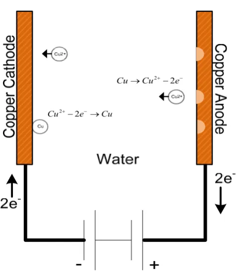
The mechanism at the anode and the cathode involves oxidation and reduction of the copper. There are three species of copper present in a copper-water based electrolytic system. They are neutral metal copper, cuprous ion copper(I) Cu1+ and cupric ion copper(II) Cu2+. These evolve from two electrochemical reactions[43, 44], as in Equation 1 and Equation 2.
However, copper(I) only evolves when the copper is not biased (as in corrosion processes) or if other contaminates are present, such as chloride. As neutral copper is not a charged ion, copper deposition is produced when copper(II) migrates from the anode depositing copper onto the cathode, as shown in Equation 3[43].
2 1
Cu +−e−↔Cu+ Equation 1
1
Cu+− ↔e− Cu Equation 2
2 2
2.2.1
Anode and Cathode
There is a great deal of confusion in some literature on the understanding of electrode polarity. The general perception is that the anode corresponds to the positive polarity and the cathode corresponds to the negative polarity. International convention[45, 46] calls the electrode where oxidation occurs the anode and the electrode where reduction occurs the cathode. The polarity on the electrodes depends on whether the cell converts electricity into chemical energy or vice versa[47, 48]. If the electrical energy is converted to chemical energy (reaction is not spontaneous), i.e. electrolysis of water to produce hydrogen and oxygen, then the anode is positive and the cathode is negative, i.e. electrons flow into the cathode. However, if chemical energy is converted to electrical energy (reaction is spontaneous), i.e. non-rechargeable battery or the phenomenon of corrosion (where no useful electrical energy is produced as it is internally converted to heat), then the anode is negative and the cathode is positive, i.e. electrons flow out of the cathode, Figure 12.
However, to reduce confusion and maintain continuity the general perception of polarity is used throughout this thesis, i.e. anode equates to positive and cathode equates to negative.
2.2.2
Electrolysis of Water
The electrolysis of water is an electrochemical process in which water decomposes into oxygen and hydrogen caused by the flow of electrons, according to the reaction shown in Equation 4.
2 2 2
2H O liquid( electrolyte)→2H ↑(gascathode)+O ↑(gasanode) Equation 4
Figure 13 – A Typical Aqueous Electrochemical Cell
Figure 13 shows a typical electrolytic cell consisting of two inert electrodes, such as platinum, with a water electrolyte, which is representative of either a large volume of water or a water drop. A potential difference is applied between the electrodes, with the anode connected to the positive terminal attracting the negative ions (anions) in the electrolyte. Similarly, the cathode is connected to the negative terminal attracting the positive ions (cations). The velocity of the ions migrating from the anode is typically a function of the viscosity of the bulk fluid, the ion radius and the electric field. For this reason it can be difficult to calculate the velocity, theoretically, for an unknown contaminate without experimentation.
Figure 14 demonstrates the large pH gradients produced at the interface of the electrodes due to the creation of the H+ and OH- ions, shown in red and blue in Equation 5 and Equation 6, respectively. At the anode the pH gradient is more acidic (pH<7) with the creation of H+ ions, while the creation of OH- at the cathode leads to a more basic pH gradient (pH >7). These pH gradients can strongly affect the corrosive properties of the metal[49]. The reaction involved for a metal exposed to moisture under a range of electric potentials and solution pH conditions are portrayed in a pH-potential (usually referred to as Pourbaix diagrams[50]), see Section 2.2.3.
Figure 14 – Demonstration of pH Gradients at the Metal Interfaces
2 2
2H O→O ↑ +4H++4e− ,O2 1.23
Anode
Eθ = − V Oxidation (Anode) Equation 5
2 2
2H O+2e−→H ↑ +2OH−
or
2 2 2O 4 4OH
O + H + e−→ −
2
,
0.83 H
Cathode
Eθ = − V Reduction(Cathode) Equation 6
Equation 5 and Equation 6 shows the half-reactions for the anode and cathode, respectively[51]. TheEAnode,O2
θ
andECathode,H2
θ
values, shown to the right of the equations, are known as the electrochemical series or standard electrode potentials (Eθ), Section 2.2.2.1. Under ideal conditions a potential of 1.23V is required to oxidise water to form oxygen gas and 0.83V to form hydrogen gas. Therefore, biasing the cell with a voltage of 1.23V would initiate redox (reduction-oxidisation). However, under real conditions decomposition of water requires larger voltages to initiate the redox reaction. This is due to a phenomenon called overvoltage, see Section 2.2.2.2, which is the additional potential required to initiate the reaction to the rate it would occur in an ideal system. The minimum practical voltage required to initiate redox of water needs to be at least 0.5V greater than the ideal voltage[51]. However, depending on material used for the electrode, the overvoltage potential can be up to 1V greater than the ideal voltage.
2.2.2.1
Standard Electrode Potentials
The standard electrode potentials are also derived from thermodynamic data and are calculated using the Nernst equation, Equation 7, with the Gibbs energy (ΔG) sourced from standard tables[52, 53].
θ nFE G=−
Δ Equation 7
Where n is the number of electrons transferred for one step of the overall reaction; F is the Faraday Constant (96,487 C mol-1) and Eθ is the electrode potential. Thus for water, n = 2 and for ΔG = -237,100 J/mol at 25ºC, which gives the electrode potential of 1.229V.
Table 2 lists the relative electrochemical potentials of metals commonly used in electronics, listed in order of their chemical reactivity, the less active at the top and the more active, or nobler at the bottom of the table. The scale of electrochemical series is used to give the degree of nobility of various electrode processes and thus is used to indicate the ability of material to ‘resist’ an electrochemical redox process, such as the corrosion process.
Metal Reaction Eθ (V)
Gold Au+ + e- = Au 1.692
Gold Au3+ + 3 e- = Au 1.498 Platinum Pt2+ + 2 e- = Pt 1.18 Palladium Pd2+ + 2 e- = Pd 0.951 Silver Ag+ + e- = Ag 0.7996 Copper Cu+ + e- = Cu 0.521 Copper Cu2+ + 2 e- = Cu 0.3419
Hydrogen 2H+ +2e- = H 0.00
Iron Fe3+ + 3 e- = Fe -0.037 Lead Pb2+ + 2 e- = Pb -0.1262 Tin Sn2+ + 2 e- = Sn -0.1375 Indium In+ + e- = In -0.14 Nickel Ni2+ + 2 e- = Ni -0.257 Cadmium Cd2+ + 2 e- = Cd -0.403 Iron Fe2+ + 2 e- = Fe -0.447 Bismuth Bi+ + e- = Bi -0.5 Tantalum Ta3+ + 3e- = Ta -0.6 Chromium Cr3+ + 3 e- = Cr -0.744 Zinc Zn2+ + 2 e- = Zn -0.7618 Chromium Cr2+ + 2 e- = Cr -0.913 Aluminium Al3+ + 3 e- = Al -1.662
Table 2 – Electrochemical Series of Metals Used in the Electronics Industry[52]
absolute values of quantitative evaluations. The differences may be due to the following[50]:
1. Some metals dissolve in the form of two simple ions (Cu+ and Cu2+) and in the form of a complex ion (CuCl2-) as opposed to the single form (Cu+), thus compounding the Eθ value and producing a misleading result.
2. Some metals may become coated with a passivating film. Yielding, for example the Eθ value for the complex Cu(OH)2 rather than the correct Eθ value for copper.
3. The additional potential added to the theoretical activation energy required for electrolysis to occur; known as the overvoltage.
2.2.2.2
Overvoltage
Overvoltage (η), in Equation 8, is the difference between thermodynamic potential, Eθ, and the practically measured potential (E) at which a noticeable current flows, i.e. the potential at which bubbles of gas appear[54]. It is the potential at which hydrogen and oxygen evolves at the cathode and anode, respectively.
The overvoltage potential is influenced by pH, temperature and other ion species in the solution, although it varies considerable with different electrode materials[55].
Material Overvoltage (V) Periodic Block Material Overvoltage (V) Periodic Block
Platinum 0.03 d Copper 0.67 d
Tungsten 0.27 d Iron 0.71 d
Smooth platinum 0.29 d Graphite 0.77 p
Antimony 0.43 p Aluminium 0.80 p
Gold 0.48 d Mercury 0.89 d
Nickel 0.56 d Tin 0.92 p
Palladium 0.59 d Zinc 0.94 d
Silver 0.62 d Lead 1.00 p
Carbon 0.64 p Cadmium 1.22 d
Table 3 – Average Overvoltage of Hydrogen on Various Metal Cathodes[54, 56] Eθ E
Table 3 [54, 56] tabulates a number of experimentally gained overvoltage values for various electrode materials. The list is compiled from various literature values and is aimed at demonstrating the affinity of overvoltage between the different materials. However, overvoltage values are normally only obtained through experimentation, because of the number of factors involved for a given system.
The highest values of overvoltage tend to be observed from s- and p-block metals such as lead and mercury, whilst the lowest tend to be observed for transition metals (d-block) such as platinum[57].
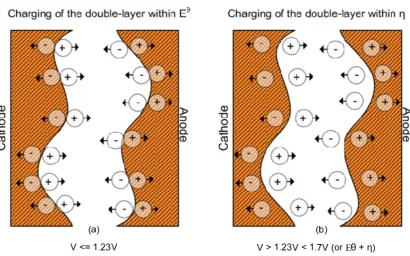
[image:41.595.114.525.353.609.2]For an aqueous cell with platinum electrodes, as in Figure 13, the voltage applied to form gas bubbles is in the order of 1.7V[54], demonstrating an overvoltage of 0.47V above the thermodynamic potential of water (Eθ), which is 1.23V.
Figure 15 – Charging of the Double-Layer within Decomposition Voltage
double-layer at the metal interface, as in Figure 15(b). However, beyond E (i.e. Eθ+η) the effective capacitance at the double layer significantly reduces as the water molecules decompose and effectively reducing the resistance.
2.2.3
Pourbaix Diagrams
[image:42.595.169.472.333.549.2]Pourbiax diagrams, named after the originator Marcel Pourbaix (1904-1998), or E-pH diagrams are plots for viewing the interrelationships between pH and potential[50]. On a Pourbaix diagram there are two axes, the Y-axis labelled E for the voltage and the X-axis labelled pH. Within the graph there are several regions that describe the function relative to pH and potential.
Figure 16 – Outline of a Pourbaix Diagram for an Aqueous Systems [50]
In the Pourbaix diagram in Figure 16 the lines (a) and (b) indicate the decomposition of water and the regions inside these lines are explained as follows:[50]
• In the region below line (a) water is unstable and will decompose to hydrogen by electrolysis at the cathode.
• In the region between lines (a) and (b) water is stable. Hydrogen is oxidised to water and any oxygen dissolved is reduced to water.
Figure 17 shows a calculated Pourbaix diagram at 25°C for copper[60] in water. These metals are commonly used in electronic manufacture with silver and gold used for connector contacts, platinum and palladium used for relay contacts, and tin and lead as the main constituents of solder.
Pourbaix diagrams are useful indicators for electrochemical failure modes, but are limited to pure elements and pure water. Therefore such diagrams may not reveal the true condition of a specific failure mode.
Figure 17 – Copper Pourbaix Diagram at 25°C[60]
2.2.4
Metal Migration Potential on Electronic Products
Metals that migrate with deionised water
Metals that migrate with deionised water and halogen contaminant
Metals that may need other conditions to migrate
Bismuth Gold Aluminium
Cadmium Indium Antimony
Copper Palladium Chromium
Lead Platinum Iron
Silver Nickel
Tin Rhodium
Zinc Tantalum
Titanium
Bias* 1-45 volts
Table 4 – ECM Condition for Different Metals Used in Electronics [61]
Figure 18, Figure 19 and Figure 20 show the Pourbaix diagrams of the metal groups in Table 4.
Figure 20 – Pourbaix Diagrams of Metals that may need other Conditions to Migrate[50]
When two oppositely polarized metal electrodes on a circuit, for example two copper tracks, are contaminated with water then electrolysed mass migration only occurs at redox, or above 1.23V. Below this voltage threshold any free ions within the contaminated-water solution will migrate to the opposite electrode and the current will decay to near zero and aid in the formation of the metal double-layer. Once the electrolysis threshold has been breached the electron flow will continue. Table 5 shows a number of Ea values of potential chemical species that may be present in a copper/water electrochemical system; such as a copper tracks contaminated by water. Note that the decomposition potential of water is 1.229V.
Species ΔG (J/mol) Ea (V)
H2O -237,100 1.229
Cu(s) 0 0
Cu+(aq) 50,000 0.518
Cu2+(aq) 65,000 0.337
CuO -129,700 0.672
Cu2O -146,000 0.757
OH
-(aq) -157,000 1.627
[image:47.595.261.390.79.209.2]Cu(OH)2 -373,000 1.939
Table 5 – ΔG [52, 53] and calculated Ea values of Typical Ionic Species when Copper is
Electrolysed in Water
It is worth noting that whilst certain other electrochemical reliability failure modes, such as dendrite growth and CAF formation, are well reported there seems to be no literature published on the potential failure effects of large capacitances caused by the double-layer on printed circuit board contamination.
2.3
Electrochemical Failures on Electronic Products
2.3.1
Dendrites
The process of dendrite growth begins with the oxidation of a metal, forming metal ions, at the anode, Equation 9, that migrate to the cathode where the metal ions then reduce back to their base metal, Equation 10[62]. This reaction is similar to the processes experienced in electroplating, although in electroplating the migrating metal ions usually plate a metal film on the cathode and tend not to form dendrites, such as shown in Figure 21.
n
Metal→Metal ++ne− Equation 9
n
Metal ++ne− →Metal Equation 10
Figure 21 – 9K x Magnification of a Dendrite Showing Fractal-like Branching
[image:48.595.237.417.383.538.2]Figure 23 – Basic Mechanism of Dendrite Formation
Metal ions produced at the anode must be able to migrate to the cathode without forming other neutral insoluble compounds i.e. non-ionised species that do not dissolve in water. Copper(I) tends to precipitate with OH- to form Cu(OH) and therefore may not form nucleation points, unlike Cu(II) which migrates from the anode without precipitation[62], and can form nuclei and start growth of a dendrite.
Most metals used as conductors can be electrochemically oxidised, including copper, gold, platinum and palladium, although gold, platinum and palladium usually require additional contaminants such as bromide, chloride and iodide ions[36, 62], as noted in Table 4. These contaminants are commonly found on printed circuit board, with bromide used as a fire retardant, and chloride and iodide used in copper etchants. Chloride and bromide are also found in solder fluxes.
process of water consist of two sets of reactions with the base reaction for the anode shown in Equation 5, with Equation 6 showing the base reactions for the cathode.
The pH of a solution is defined as the inverse log of the H+ ion concentration, i.e. –log [H+], and thus the pH level experienced at each electrode differs as a function of H+ production. This can be seen in the reactions in Equation 5 and Equation 6 with the production of H+ at the anode forming a more acidic solution and at the cathode with the production of OH- ions forming a more basic solution, i.e. more OH- than H+. However, the final pH at the electrode interface also depends on the contamination present such as sodium and potassium carbonate from the basic solder mask developer[65] and weak organic acids found in solder fluxes, shown in Table 1.
An experimental study[64] into the effects of pH on dendritic growth in saturated conditions indicates dendritic growth is accelerated by decreasing the pH below pH 5, with higher pH suppressing growth, although signs of solid corrosive products may be observed between the anode and cathode. The study explains that a fractal formation of a dendrite, i.e. shape, size and overall characteristics, changes notably if anionic contaminants, such as Cl-, are added to the electrolyte, i.e. water. Another source[66] suggests a similar change to the dendrite shape, where an increase in the concentration gradient reduces the fractal nature of the dendritic growth, as in Figure 24.
Figure 24 – Dendrite Shapes as a Function of Concentration Gradient[66]
fuse and the current leakage is either reduced or disappears. However, over time the dendrite filament will thicken and the current may increase sufficiently to produce circuit failures [68, 69].
With lower current circuits, such as microprocessor data buses, these dendrite bridges can be problematic. The failures caused by the formation of dendrites are not normally intermittent, i.e. they are either fully open or fully short, and for this reason it can be difficult to detect dendrites especially if they have been blown-out.
Available papers dealing with the effects of dendrites at varying temperature within normal operating conditions of commercial electronics are limited. This is probably due to a combination of the long durations required for each experiment (at humidity less than saturation) and the emphasis on standard testing, i.e. 1800 hours,(rather than operating) conditions, with most electrochemical migration validation testing limited to comparatively high temperatures of 85°C/85% RH exposure[21, 23]. Wassink[26] generalised that the chance of dendrite growth is a function of the Arrhenius equation, which is shown in Section 2.5.
2.3.1.1
Electrochemical Growth Models
Theoretical growth models that reflect the behaviour of failure mechanisms such as dendritic growth tend not to reflect the failure conditions experienced in the field. The most accurate models are those produced from experimental data that determine the quality of fit, which is generally not perfect. The reason is the unseen variables that are not considered and which can play a significant role in the end result[70]. The quality of the data depends on the material quality and the experimental control.
shown in Figure 25[49]. Here positive metal ions are formed at the positively biased electrode (the anode), and migrate toward the negatively charged cathode.
[image:52.595.120.532.141.393.2]Figure 25 – Overview of Electrochemical Migration [49]
Figure 26 – Micro-steps [72]
concentrated electric field at a projection; producing a faster growth than on a flat surface.
Figure 27 – Representation of a Concentrated Electrical Field [71]
In his second theory Bockris explains the mechanics of dendritic growth under the heading of dendrites; loosely termed the elementary theory of dendrite formation. This theory seems to complement the previous theory that under the ‘right conditions’ the next step, after the growth of a metal deposit, is to form a dendrite. However, Bockris does not make this connection obvious.
Figure 28 – The Nernst Diffusion-layer Thickness (δ)
Di Giacomo [73] explains that for the production of a metal dendrite, the current density at the whisker’s tip must be several orders of magnitude higher than the average current. The growth is possible through spherical diffusion ‘focusing’ the ionic current on the dendrite tip, which can be expressed in terms of its radius of curvature.
The electric field can be calculated from the voltage bias, which, in turn, is directly proportional to the force applied on a charged particle (e.g. a metal ion) within the field[74]. The force applied on a charged particle may affect the time it takes an ion to move through the electrolyte. The electric field can be calculated from the applied voltage and electrode geometry under consideration. In its simplest form the field in a parallel plate capacitor is expressed by, E=V/d where E is the electric field, V is the applied voltage and d is the distance between the two oppositely biased plate electrodes[75].
2.3.2
Conductive Anodic Filaments (CAFs)
are used. However, the chemical composition of the laminates and processing materials, humidity, and voltage bias are also understood to aid in their formation[79]. The formation of a CAF is the result of an electrochemical migration process that initiates at the anode. In contrast to dendrites forming from the cathode, CAF growths emanate from the anode inside the printed circuit board epoxy fibres and contain a combination of materials such as halide ions to form copper salts[22, 30, 79]. These growths tend to form between vias, also known as printed-through holes, and can potentially migrate to a more cathodic via and form a short circuit, shown in Figure 29.
Figure 29 – Schematic of a CAF Pathway between Two Vias
cathode (Equation 5 and Equation 6). If these pH gradients either propagate or the pH diffusion regions are in close proximity, for example closely spaced vias, then essentially these extreme pH concentrations can form salts (i.e. base+acid = salt). The simplified copper Pourbaix diagram[50], in Figure 30, shows that with a pH below 7 and a potential greater than 0.2V copper corrosion can occur. In a CAF, as the anode produces copper ions (Cu2+), migration occurs towards the cathode, which remains virtually stable at all pH levels. As the copper ions migrate they move towards the cathode, a more basic region, and the pH increases above 5 where the corrosion process starts to declines. At approximately pH 8.6 the copper product becomes insoluble[69], forming stable conductive copper salts that emanate from the anode acting as conductive paths and potentially electrically shorting the biased vias.
40
2.3.3
AC Formations
Literature searches have not revealed any published work that directly cites results using AC (alternating current) ECM (electrochemical migration) testing or AC ECM reliability issues for printed circuit boards. This is clarified in a communication with Neves[80] and a meeting with NPL. Neves comments in one of his articles[81] that there are some movements in Europe towards the use of AC power sources in ECM testing.
In correspondence, Neves explains that his comments in the article are founded on general discussions on CAF testing with members of the IEC (International Electro-technical Commission), in his role as chairman of the working group for Test Methods for Printed Circuit Boards & Materials. Within this working group they discussed the creation of methods for the IEC 61189[82] standard. In this correspondence, Neves also clarifies that they too have not found published work in the field of AC in ECM testing. His group feels this may become an area that should be noted and thus his comments in his article.
In a further communication with Neves [83] he indicates an interest in understanding (empirically) how AC voltages influence ECM, both with, and without, a DC bias, and an interest in comparing the results with the present DC ECM test methods. The author later found the sole European interest was actually the NPL funded by the DTI (Department of Trade and Industry).
Examples of dendrites grown with an AC bias are shown in Figure 32, with the left image showing a dendrite grown at ±2v 0.0001Hz and the right image showing a double tailed dendrite grown at ±2v 0.1Hz. As these dendrites are grown at sub-hertz frequencies it could be said the bias used is pulse DC as opposed to AC, effectively operating as a DC electrochemical cell. However, formations grown at frequencies greater than 10Hz do not produce dendrite-like structures, but rather powder-like growth at both the anode and the cathode.
Figure 32 – AC Dendrite Growth (a: 0.001Hz, b: 0.1Hz)
This is further detailed by Hamann [72] where he explains the application of an AC potential to a cell. Due to the rapidly changing potentials, the various processes at the electrode surfaces are forced to oscillate with an applied frequency above 1Hz. The process of redox will also oscillate although the greater the distance from the electrode the more dampened the concentration changes. If there is no DC offset to the AC signal then the cell may not form growths such as dendrites. However, a DC offset will encourage a net current flow and thus increase the chance of dendrite formation.
Figure 33 – Diffuse, White or Blue-green Residue on AC Circuits
The image shown in Figure 32 seemingly demonstrates dendrite growths under AC conditions. However, the definition of AC needs to be considered in the case of electrochemical migration. The growth on Figure 32(a) is formed at a frequency of 0.0001 Hz, which is equivalent to 10,000 seconds for one complete cycle. The cell is exposed to a peak voltage of 2V twice per cycle, once at 2,500 seconds and again at 7,500 seconds. The growth of the dendrites probably occurred during these intervals, which is also suggested by Chan [84]. Thus, the dendrites effectively grew under DC conditions, i.e. above 1.23V demonstrated in Experiment 2 in this thesis.
Chan [84] suggests an AC SIR (Surface Insulation Resistance) approach which may pose several advantages as an alternative to DC SIR. Firstly, the disturbance to the ion distribution of the systems due to the measurement itself is minimised, i.e. under DC ions distribute evenly at the electrodes reducing the resistance. Secondly, voltage accelerated experiments may be possible, as in theory no net migration will occur.
is the case, each half cycle that is favourable for the reaction will still accelerate the ions toward the opposite electrode possibly due to the inertia. This can be considered as similar to the theoretical model shown in Figure 31, however, at the appropriate activation potential the anode loses hold on the ion and accelerates it towards the cathode, i.e. the AC field creates momentum and the hysteresis over shoots the field strength and accelerates the ion towards the cathode.
From the frequency tests Chan conducts, the AC current stays stable for several hours. However, over longer time periods the SIR decreases slowly, and steadily, to 2-3 times less than the initial value after 150 hours. A point worth noting in these results is that the SIR does not increase at all under the AC bias.
Compared to DC SIR, Chan’s results demonstrate the potential advantages of AC measurements. On a DC system the electrodes are fixed and there is a known cathode and anode polarity. In this type of system the pH levels differ towards either an acid, H+ migration, for the cathode or an alkaline, OH-, migration, for the anode. With an AC system there could be various interactions and this could have implications for the residual salts left in the electrolyte and could explain the images in Figure 33.
Yin also finds the frequency range used affects the results. Another point for noting is that high quality deposition of nickel can be obtained with AC frequencies from 10 to 750 Hz and for bismuth the optimum frequency range is between 10 and 100 Hz.
The reason for the difference seen as the frequency changes is unclear. However, Yin compares this to a similar phenomenon seen in pulse electroplating, which the acceleration effect to the opposite electrode could therefore facilitate the growths. The effects of frequency on the deposition could also be explained by the difference in particle size, in that bismuth is a heavier metal than nickel; i.e. if the effect of simple harmonic motion on a molecule is considered, it can be concluded the rate of oscillation will be dependent on the mass. Thus a particle that has a larger mass will vibrate slower than a lighter particle.
The paper does highlight the difference could be associated with the double layer capacitance which is a function of the AC frequencies. However, if the electrodes are of the same size for both materials (bismuth and nickel) then why would the double layer capacitance have such a difference? Further investigation is needed to ascertain more data and a fuller understanding of the double layer and its effects with different metal and electrolytes.
Yin’s paper is not unique and there have been several other papers published describing AC electrodeposition [86, 87], albeit most on the formation of nano-wires.
From the literature search it is evident that the effects of AC on the process of electrochemical migration are significant and it does show that some formations with AC may happen, under the right conditions, on PCBs.
46
2.4
Methods for detecting ionic migration
The detection of electrochemical migration is traditionally conducted using a standard industrial technique termed Surface Insulation Resistance (SIR) and executed within a given standards, a number of which are shown in Table 6.
Standard IEC 61189-5 (in draft) IOS 9455-17 (latest) J-STD-001C IPC-TM-650 2.6.3 IPC-TM-650 2.6.3.3 Bellcore
Temperature/
Humidity 40°C/93%RH 85°C/85%RH
85°C/85% RH
Class 1:35/90°C at 98%RH for 4 days
static. Class 2:50/90°C at
98%RH for 7 days static. Class 3:25/65°C at 90/98%RH for 7 days
cycling.
85°C/85%RH 35°C/85% RH
Test Duration 72 hours 168 hours 168 hours 168 hours 168 hours 120 hours
Measurement Frequency
20 min intervals
Twice in 24 hour period
24 hrs, 94 hrs and 168
hrs
24 hr intervals hrs and 168 24 hrs, 94 hrs
25 hrs and 120 hrs
Test Voltage 5v 50v 100v 100v 100v 100v
Bias +5v +50v -50v -50v -50v -50v
Test Coupon Review Under IPC-B-24 IPC-B-36 IPC-B-25A IPC-B-24 IPC-B-25A
Table 6 – Summary of SIR Standards and Some Parameters
A number of factors can influence the phenomenon of electrochemical migration with some of these factors listed in Table 7.
Item Factors
Conductors -Nature of the metal or alloy -Surface condition/roughness -Conductor configuration -Conductor spacing
Substrate -Composition and moisture absorptivity -Structure
-Reinforcements and their nature
Atmosphere -Temperature -Humidity
-Corrosive elements and their concentration -Electrical conductivity of the medium -Air velocity
Operating Conditions -Electrical potential -Temperature -Humidity
Table 7 – Factors that can Influence Electrochemical Migration
decreasing these factors can be thought of as increasing and decreasing the diameter of the circles.
Figure 34 – Venn Diagram of Electrochemical Failure Modes
The following Sections describe current test methods for detecting the presence of electrochemical migration on printed circuit boards.

![Table 1 – Typical Composition of Rosin[14, 36, 37]](https://thumb-us.123doks.com/thumbv2/123dok_us/8731721.887081/31.595.255.401.566.661/table-typical-composition-of-rosin.webp)
![Figure 16 – Outline of a Pourbaix Diagram for an Aqueous Systems [50]](https://thumb-us.123doks.com/thumbv2/123dok_us/8731721.887081/42.595.169.472.333.549/figure-outline-pourbaix-diagram-aqueous-systems.webp)
![Figure 19 – Pourbaix Diagrams of Metals that Migrate with Deionised Water[50]](https://thumb-us.123doks.com/thumbv2/123dok_us/8731721.887081/45.595.143.509.92.442/figure-pourbaix-diagrams-metals-migrate-deionised-water.webp)
![Figure 20 – Pourbaix Diagrams of Metals that may need other Conditions to Migrate[50]](https://thumb-us.123doks.com/thumbv2/123dok_us/8731721.887081/46.595.136.521.89.319/figure-pourbaix-diagrams-metals-need-conditions-migrate.webp)
