Code Size Reduction in Embedded Systems with
Redesigned ISA for RISC Processors
Govindarajalu B,
B S Abdur Rahman University, Vandalur, Chennai -600048,
India
K.M.Mehata,
PhD. B S Abdur Rahman University,Vandalur, Chennai-600 048, India
ABSTRACT
Reducing the size of a program is a major goal in modern embedded systems. Large code occupies more space in the Chip and also causes higher power consumption because of increased memory traffic. In this paper, a revised architecture is proposed for embedded processors by replacing the Load-store Architecture with Register-Memory Architecture for selected instructions. Analysis of RISC object code for Embedded Applications, using an offline tool developed by the authors, establishes the scope for a new class of processor exclusively for embedded applications. We have used this tool to simulate Register-Memory Architecture for MIPS processor. Based on the results, MIPS processor's instruction set is enhanced with 12 new instructions of Register-Memory Architecture. Experimental results for MiBench Benchmark programs with Register-Memory Architecture Simulation reveal that code size reduction up to 22% can be achieved with modified MIPS Architecture. This is also applicable for microMIPS processor that claims 35% code space saving with 16-bit instructions, thus offering a total of over 55% code space reduction compared to MIPS32 Architecture, for embedded systems. Equivalent memory reduction achieved is very significant for Embedded Systems built using SOCs. Processor design modifications, required at microarchitecture level, are also identified. Other additional features that can be combined with Register-Memory Architecture for an efficient embedded processor are identified.
General Terms
Computer Architecture, Embedded Systems
Keywords
Embedded system, power consumption, code size, RISC, Code compression, Chip space
1.
INTRODUCTION
An embedded system usually performs a dedicated function, and is generally non-programmable by users. Use of embedded systems has increased rapidly in several applications, ranging from small hand held products to sophisticated medical equipments and aerospace. Though performance is important, it is not critical in several embedded systems such as cameras, video game consoles, TV remote controls, cell phones, personal data assistants (PDAs), and toys. Instead, cost, power consumption and physical dimensions are the critical factors.
Embedding multiple processor cores in single system-on-a-chip (SOC) is a modern design practice that offers lower design cost, reduced time-to-market and design reuse. The code size is one of the factors that affect the chip space and power consumption since the program memory is on-chip in most embedded systems. If the code size increases, number
of instructions fetched also increases thereby increasing the power consumption. High power consumption also leads to increased operating temperature since it is not practical to use cooling fans in most embedded systems. Operating these systems for long duration may also cause reliability problems apart from reducing the battery life. Considering these issues, it is essential that processor designers need to suitably modify the existing RISC processors thereby making them more suitable for embedded systems. The following discussion explains why present day RISC processors contribute to increased power consumption.
1.1 Code size and RISC Processors
Table 1. Frequency of Data Transfer Instructions in Typical CISC and RISC Processors
Program Processor ALU instructions
Data
transfer instructions
gcc VAX 40% 19%
gcc MIPS 35% 27%
spice VAX 23% 15%
spice MIPS 29% 35%
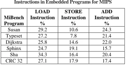
The code bloating problem is more critical for embedded systems thereby requiring serious efforts to minimize it. The frequency of usage of LOAD and STORE instructions in MIPS object codes for embedded systems has been estimated by the authors with the MiBench Benchmark programs. The MiBench is a popular suite that is widely used for evaluating the behavior of embedded systems. Table 2 lists the percentage distribution of LOAD, STORE and ADD instructions for six different MiBench programs compiled using SimpleScalar simulator and analyzed using an offline instruction distribution analyzer tool developed by the authors. From these measurements, it is obvious that the LSA Architecture is a burden on Embedded Systems.
TABLE 2. Distribution of LOAD, STORE and ADD Instructions in Embedded Programs for MIPS
MiBench Program
LOAD Instruction
%
STORE Instruction
%
ADD Instruction
%
Susan 29.2 10.6 24.3
Typeset 27.2 7.8 21.4
Dijkstra 25.8 14.6 22.0
Sphinx 24.7 19.1 15.7
Sha 34.3 16.4 20.4
CRC 32 27.1 17.9 17.4
Register-Memory Architecture and Hybrid Instruction Encoding (HIE) are two features that can substantially reduce code size. The authors are working on developing a new Hybrid Embedded Processor Architecture (HEPA) that supports both RMA and HIE so that future embedded systems based on SOCs are free from code bloating problem and are inherently low power enabled. The goal of this paper is to estimate the scope for RMA for existing RISC processors to achieve maximum reduction of code size and chip space. This paper deals with modifying an existing RISC architecture with new RMA arithmetic/logical instructions to minimize the number of instructions in the code. The rest of the paper is organized as follows. In section 2, we present related work on code size reduction. Section 3 describes the impact of RMA on Embedded Processors. Section 4 explains the methodology used for introducing RMA in existing RISC processors and relevant pipeline changes. Section 5 gives sample measurements estimating the resulting code space reduction due to ISA modifications. Section 6 presents the conclusions and proposes an alternate solution for processor developers.
2.
RELATED WORK
To reduce code size, several techniques have been implemented [2]. These are classified into three types [3]: Code compression, Compiler techniques and ISA
whereas the third technique involves supporting a new instruction set that is a subset of the original ISA. The technique proposed in this paper is a variant of the third technique with a superset of the original ISA. An overview of these three techniques is given below.
2.1 Code compression
Code compression involves compressing the RISC object code, in offline, based on some compression algorithm and storing the compressed code in main memory and decompressing it by hardware, on-the-fly, during program execution. The decompression unit is placed between the processor core and memory due to which there is an increase in chip space [4]. Wolfe and Chanin [5] were the first to apply code compression to embedded systems. Their scheme known as Compressed Code RISC Processor (CCRP) uses Huffman coding to compress MIPS object codes. This method established the foundation for the IBM Codepack compression technology for the PowerPC 400 series [6]. This approach does not involve compiler modification or processor design change. Dictionary- based compression is another compression method [2]. It is based on the property that the same instructions frequently reappear in the object code. A dictionary table maintains a list of distinct instructions in the application program. Then the instructions in the program are replaced by their respective indices to the dictionary. During instruction fetch, reference to the dictionary using the index, gives the actual instruction that will be supplied to the processor. Though this is a simple technique to implement, the solution is not application independent since the developer has to profile the given object code and generate a dictionary table that is unique to the given application.
2.2 Compiler Techniques
Compiler techniques [7] for code compression involve register renaming, interprocedural optimization, and procedural abstraction of repeated code fragments. The procedure abstraction is a program optimization that replaces repeated sequences of common code with calls to a single procedure. These techniques have no runtime decompression overheads and do not require any hardware change since the code generated can be directly executed by the processor. However, there is a need to modify the software tools such as compilers and linkers.
2.3 ISA Modification
[image:2.595.57.277.373.486.2]registers. Some of the 16-bit microMIPS instructions can access only 8 of 32 GPRs.
The approach in this paper resolves these weaknesses. It does not remove any instruction from the original instruction set. On the other hand, this paper introduces 12 new RMA instructions. As a result, the instruction set is marginally enhanced. Though compiler and processor modifications are required, these are one time efforts by the processor manufactureres/ compiler developers and there is no burden on embedded system developers as required for other approaches. Also it is a program independent solution for embedded applications. This strategy can be combined with other methods of code size reduction thereby achieving additional amount of code size reduction.
3. IMPACT OF RMA ON EMBEDDED
PROCESSORS
Generally, RISC processors [11] have three types of instructions: ALU instructions, Load and store instructions and Branch and Jump type instructions. For ALU instructions, the operands are in registers and the results will be stored in registers. In Load and Store instructions, one operand is in register and the other operand is in memory. Our proposal is to support one memory operand in 12 different ALU instructions, thereby adding a new class of register-memory instructions in addition to existing register-register ALU instructions. This will impact the processor design as regard to opcode decoding and pipeline design. Apart from redesigning the processor cores, modifications are required in the existing compilers and associated program development tools.
The hardware changes for supporting the RMA arithmetic/logical instructions will cause performance penalty to processors, to some extent, making them less attractive for some market segments such as servers and workstations. Therefore, bringing out a separate processor model/version for embedded market may be the best choice in view of ever growing population of embedded systems. The authors have evaluated the feasibility of incorporating RMA arithmetic/logic instructions in existing RISC processors and a case study is presented for MIPS processor in the next section.
4. METHODOLOGY - IMPLEMENTING
RMA ALU INSTRUCTIONS
This section describes the design steps involved in redesigning the existing RISC processors to support the RMA ADD (ADDrm) instruction. A specific case of MIPS processor is considered and a scheme for including 12 new RMA ALU instructions is presented occupying the vacant slots in MIPS instruction set. The following steps are involved in modifying RISC processors for including the RMA instructions:
1. Assign vacant opcodes to the RMA instructions 2. Choose formats for the RMA instructions
3. Modify pipeline sequence to suit the RMA instructions 4. Review the need for additional data path and controls 5. Modify the controls to support hazards and interrupts We have discussed here using the examples of ‘add’ type instructions. However, the implementation procedure applies for other arithmetic/logical instructions also.
4.1 MIPS Instructions
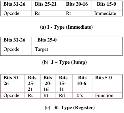
The original MIPS I CPU ISA has been extended in a backward-compatible fashion several times: MIPS II, MIPS III, MIPS IV and microMIPS. Each new architecture level (or version) includes the former levels described in MIPS website [12]. The discussions below restrict to integer instructions of MIPS to maintain simplicity. Figure 1 shows the three different instruction formats used by MIPS processor.
Bits 31-26 Bits 25-21 Bits 20-16 Bits 15-0
Opcode Rs Rt Immediate
(a) I - Type (Immediate)
Bits 31-26 Bits 25-0
Opcode Target
(b) J – Type (Jump)
Bits 31-26
Bits 25- 21
Bits 20- 16
Bits 15-11
Bits 10-6
Bits 5-0
Opcode Rs Rt Rd 0’s Function
[image:3.595.315.533.163.362.2](c) R- Type (Register) Fig.1 MIPS Instruction Formats
Addition is available both in R-Type format and I-Type format as shown in Fig.2 and Fig.3 respectively. In R-type addition, both the source operands (Rs-r and Rt-r) are available in registers and the result is placed in the destination register Rd-r. In I-type addition, one source operand is in a register Rs-i and the other source operand is available in the instruction as immediate operand. The result is stored in the destination register, Rt-i. MIPS document [12] gives the entire instruction set of MIPS, also indicating the unused opcodes.
OP (Bits 31-26)
Bits 25- 21
Bits 20- 16
Bits 15-11
Bits 10-6
Bits 5-0
[image:3.595.316.524.477.638.2]0’s Rs-r Rt-r Rd-r 0’s 100000
Fig. 2 R-Type ADD Instruction
.
Opcode
(bits 31-26)
Bits
(25-21) Bits
(20-16)
Bits
(15-0)
001000 Rs-i Rt-i Immediate
Fig.3 I-Type ADD Instruction
4.2 Formats for ADDrm Instruction for
MIPS
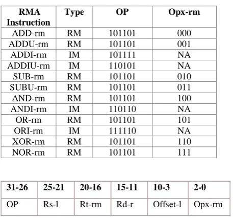
Table 3 lists 12 new RMA instructions. Figures 4 and 5 show the suggested formats for these instructions. Both R-Type and I-Type instruction formats are possible for the ADDrm in MIPS. Strategy used by the RMA simulator to modify the R-Type and I-R-Type ADD instructions, to generate corresponding RMA instructions, is discussed in section 4.5.
4.2.1 Using R-Type Format
We use Rs-r as a base register and the 8-bit offset to specify the memory operand. The register operand is in Rt-r. This will require a new datapath for bits 10-3 of instruction register to the adder input. Relevant additional control signals have to be generated by the opcode decoder. We have retained the 3- address format.
4.2.2 Using I Format
Use Rs-r as a base register and the 8-bit offset to specify the memory operand. The immediate field gives the other operand. For generating memory address, the existing data path for load type instructions can be used.
4.3 Impact of RMA Opcodes
[image:4.595.53.282.432.645.2]As seen in Table 3, and figures 4 and 5, the RMA instructions introduce two new formats. The 3-lsbs (bits 2-0) define the nature of operation whereas the 6-msbs (bits 31-26) gives the operation type, for RM format. For IM format, the 6-msbs alone indicate the operation. The offset and immediate fields are only 8-bits that may pose a challenge to the compiler. As discussed in section 4.5, MIDACC converts LSA instructions into RMA instructions only if the length limitation is satisfied.
TABLE 3. 12 New RMA Instructions (op- main opcode; opx-rm - opcode extension; NA - not applicable)
RMA Instruction
Type OP Opx-rm
ADD-rm RM 101101 000
ADDU-rm RM 101101 001
ADDI-rm IM 101111 NA
ADDIU-rm IM 110101 NA
SUB-rm RM 101101 010
SUBU-rm RM 101101 011
AND-rm RM 101101 100
ANDI-rm IM 110110 NA
OR-rm RM 101101 101
ORI-rm IM 111110 NA
XOR-rm RM 101101 110
NOR-rm RM 101101 111
31-26 25-21 20-16 15-11 10-3 2-0
OP Rs-l Rt-rm Rd-r Offset-l Opx-rm
Fig. 4 RMA Instruction Format – RM Type
31-26 25-21 20-16 15-8 7-0
OP Rt-i Rs-l Offset-1 Immediate
Fig.5 RMA Instruction Format – IM Type
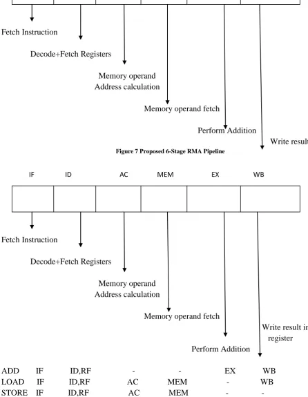
4.4 Pipeline modifications for supporting
RMA instructions
A five stage instruction cycle sequence shown in Fig.6 is commonly followed in RISC processors [11]. An instruction is active at any instant in only one of the stages. During IF, the instruction is fetched from the code memory. During ID, instruction decoding is done and also register operands are fetched. During EX, either instruction execution or address calculation is done depending on the instruction type. During MEM, data memory is accessed if relevant. During WB, the result (if applicable) is stored in a register.
IF ID EX MEM WB
Figure 6. Typical 5-stage RISC Instruction Sequence
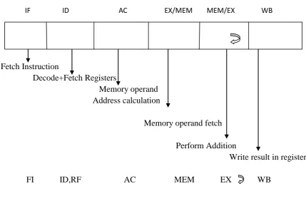
The traditional RISC pipeline sequence has to be rearranged to suit both LSA and RMA instructions, interchanging the Data memory access and Execute stages. Fig.7 shows a proposed 6-stage pipeline that supports the RMA Register-Memory instructions, for RISC processors.
Let us consider the pipeline action for the ADD-RM instruction. The first two stages are similar to the RISC pipeline. In the third stage (AC), memory address, for the memory operand, is calculated by a small address adder (as in ARM processors) and in the fourth stage (MEM), the memory operand is fetched from the data memory. In the fifth stage (EX), addition is carried out and in the last stage (WB), the result is stored in destination register.
Fig.8 shows the execution of LSA instructions in the new pipeline. For the LSA ADD instruction, the AC and MEM cycles are unused. Compared to a 5-stage RISC pipeline, one additional clock cycle is wasted (consumed) for LSA instructions in the 6-stage RMA pipeline.
The unused internal cycles [13] do not directly affect performance, since they do not cause pipeline stalls. However, a slight performance decrease is expected due to increase in pipeline length in view of increased frequency of dependencies between successive instructions. It is a question of choice between performance and code size. For embedded systems, code size is more significant, and hence the increase in execution time by one cycle is tolerable. An alternate approach is possible for the RMA pipeline with 5 stages as shown in fig. 9 in which the EX and MEM stages are combined as a single MEM/EX stage to improve the efficiency of the RMA pipeline for the LSA instructions.
In the 6-stage pipeline, the EX stage is unused by LOAD and STORE instructions of LSA, and the MEM stage is unused by LSA ADD instruction as shown in Fig.8. Hence in the 5-stage RMA pipeline, the EX and MEM stages are combined into a single MEM/EX stage. Therefore, no performance penalty is caused for LSA instructions. For the ADD-rm instruction, the MEM/EX stage is recycled as shown in Fig.10. In the first MEM/EX cycle, the memory operand is fetched from the data cache and, in the second MEM/EX cycle, the addition is performed As a matter of fact, such 5-stage approach has been used in several processors including Pentium, R8000 and PA 7100 [13] .
IF ID AC MEM EX WB
Fetch Instruction
Decode+Fetch Registers
Memory operand
Address calculation
Memory operand fetch
Perform Addition
Write result
Figure 7 Proposed 6-Stage RMA Pipeline
IF ID AC MEM EX WB
Fetch Instruction
Decode+Fetch Registers
Memory operand
Address calculation
Memory operand fetch
Write result in
register
Perform Addition
[image:5.595.52.499.127.703.2]ADD IF ID,RF - - EX WB
LOAD IF ID,RF AC MEM - WB
STORE IF ID,RF AC MEM - -
IF ID AC MEM/EX WB
Fetch Instruction
Decode + Fetch Registers
Memory operand
Address calculation
Memory fetch/write +
Perform Addition Write result in
register
ADD IF ID,RF - EX WB
[image:6.595.59.505.115.355.2]LOAD IF ID,RF AC MEM WB
STORE IF ID,RF AC MEM -
Figure 9 Execution of LSA Instruction in 5 – Stage RMA Pipeline
IF ID AC EX/MEM MEM/EX WB
Fetch Instruction
Decode+Fetch Registers
Memory operand
Address calculation
Memory operand fetch
Perform Addition
Write result in register
[image:6.595.59.489.443.746.2]4.5. Simulation of RMA Instructions
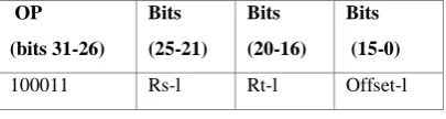
The extent of code size reduction due to the use of RMA Arithmetic instructions depend on the frequency of generation of these instructions by the new compiler. This also varies with the nature of embedded programs. Simulation studies have been performed with the MiBench benchmark programs for estimating the code size reduction. The authors have developed a software tool named MIDACC to simulate the RMA environment. This tool scans the MIPS compiler output and estimates the scope for RMA instructions in the given program by a search for appropriate sequences of Load word (LW) and ALU instructions. The format of LW instruction is shown in Fig.11.
OP (bits 31-26)
Bits
(25-21) Bits
(20-16) Bits
(15-0)
100011 Rs-l Rt-l Offset-l
Figure 11 Format of LW Instruction
The MIDACC inserts RMA Instructions by performing the following actions a-e:
(a) Scans the input code for a ‘special two-instruction’ sequence of LOAD WORD (LW) followed by ALU type (such as ADD) instruction with a common operand. Combinations of the LW instruction immediately followed by any of the 12 ALU instructions are considered.
(b) Deletes the identified LW instruction and the immediately following ALU type instruction if they satisfy some operand combinations between these two instructions.
Qualifying conditions for LW followed by R-Type ALU Instruction:
1. Numeric value of ‘Offset-l’ should not occupy more than 8-bits.
2. Rt-l should be equal to either Rs-r or Rt-r. If Rt-l is equal to Rs-r, Rs-r is dropped and Rt-r is renamed as Rt-rm. If Rt-l is equal to Rt-r, Rt-r is dropped and Rs-r is renamed as Rt-rm. Qualifying condition for LW followed by I-Type ALU Instruction:
1. Numeric value of ‘Immediate’ should not occupy more than 8-bits.
2. Rt-l should be equal to Rs-i. If it is equal, the Rs-I is dropped.
(c) Creates a new RMA instruction in the original location for LW instruction. The RMA instruction is also of 32-bits as shown in Figures.
The steps (a) to (c) are repeated for the entire program till all LW-12 ALU sequences are covered.
5. RESULTS AND DISCUSIONS
MIDACC was used by the authors to simulate the RMA environment for running MiBench Benchmarks that are a collection of C programs for six different embedded applications. The experiments were conducted in Intel PC under Linux. The authors used SimpleScalar simulator for cross compilation. The compiler output is analyzed by MIDACC for estimating the scope for RMA in the given program. In addition to inserting the RMA instructions, it also generates the compressed code that can be used as input to the linker. Table 4 lists the results obtained by us for six selected embedded programs.
As already mentioned, the code reduction by RMA is additional reduction that can be combined with other techniques. Hence
effective percentage reduction for the MiBench programs taking into account RMA for microMIPS architecture varies from 41.4 (consumer applications) to 55.1 (Network applications). The Automotive and Industrial Control applications will see 52.8 % code size reduction. This results in proportional chip space savings and equivalent power reduction.
6. CONCLUSIONS AND FUTURE WORK
This paper advocates implementation of register – memory architecture for embedded processors for low power embedded systems in view of the need for reduced chip size and lower power consumption. Encoding of appropriate new instructions and pipeline modifications of existing RISC processors to support RMA arithmetic/logical instructions is recommended. A case study has been presented demonstrating addition of 12 instructions for MIPS. The measurement with the C programs in MiBench suite gives over 20% of code space reduction. This is an additional savings in addition to other techniques of code space reduction. Combining the RMA technique with microMIPS Architecture will yield over 55% code size reduction.
Designing a new processor is the answer to the needs of embedded systems. A study of existing RISC processors gives a clue to the specifications of a new processor. The instruction format affects the code size and the processor performance. While choosing the instruction formats, the processor architect considers [1], [14] following factors: code size, processor design complexity, processor performance and compiler complexity. The number of registers and the addressing modes affect the length of the instruction and compiler simplicity. Similarly the number of operands per instruction affects the instruction length and code size. The instruction size, number of instruction formats and addressing modes determine the complexity of instruction decoding and the difficulty of pipelining. The number of registers determines the extent of help to the compiler to generate efficient object code.
[image:7.595.64.267.216.270.2]The authors are presently working on upgrading the MIDACC and simulate the proposed HEPA.
TABLE 4. Code Size Reduction in RMA for MiBench
Applicati-on
Progra-m
No. of Instru-ctions
A
No. of Load cases
B
RMA cases
C
% Reduc -tion
C/A
Automoti-ve and Industrial
Control
Susan 12502 3655 2228 17.8
Network Dijkstra 418 108 84 20.1 Telecom CRC 32 195 53 24 12.3 Security Sha 538 185 57 10.6 Office Sphinx 89 20 7 7.9 Consumer Typeset 5598 1523 357 6.4
studies using SimpleScalar tools to determine the optimum configuration of the desired Embedded Processor.
7. ACKNOWLEDGMENTS
The authors would like to thank Raysoft professionals, Mr. S.Raju, CEO and Mr. S. Ramkumar, Programmer, for their suggestions during development of MIDACC. Thanks are also due to Dr. V.P.Ramamurthi, Chairman, Dhanalakshmi College of Engineering for extending the research facilities, and Mrs. Shyamala Dharmar, CEO, Vael's Academy, for her suggestions towards effective presentation.
8.
REFERENCES
[1] J.L.Hennessy and D.A.Patterson, “Computer Architecture: A quantitative Approach”, Fourth edition, Morgan Kaufmann publishers, 2007.
[2] J. Heikkinen, J.Takala, and H.Corporaal, “Dictionary based program compression on customizable processor architectures”, Microprocessors and Microsystems, vol. 33, pp. 139 – 153, 2009.
[3] Y. Xie, W. Wolf, H. Lekatsas, “Code Compression for VLIW Processors using Variable – to- Fixed Coding,” IEEE Trans. VLSI Systems, vol. 14, no.5, pp. 525 – 536, May 2006.
[4] L.Benini, F.Menichelli, and M.Olivieri, “A class of code compression schemes for reducing power consumption in embedded microprocessor systems”, IEEE
Trans.Computers, vol.53, no.4, pp.467 – 482, April 2004. [5] A. Wolfe and A. Chanin, “Executing compressed programs on an embedded RISC architecture”, in Proc. Int. Symp. Microarch, 1992, pp.81 – 91.
[6] T.M.Kemp, R.K. Montoye, J.D. Harper, J.D.Palmer, and D.J. Auerbach, “A decompression core for power PC,” IBM J.Res.Develop., vol.42, no.6, pp. 807 – 812, Nov. 1998.
[7] J.A. Fisher, P.Faraboschi, and C.Young, “Embedded Computing: A VLIW Approach to Architecture, Compilers and Tools”, Morgan Kaufmann publishers, 2005.
[8] A.N.Sloss, D.Symes and C.Wright, “ARM System Developer’s Guide: Designing and optimizing System Software”, Morgan Kaufmann Publishers, 2004.
[9] C.H.Lin, Y.Xie, and W.Wolf,”Code Compression for VLIW Embedded Systems using a self-generating table”, IEEE Trans. VLSI Systems”, Vol.15, no.10.pp.1160-1171, Oct.2007.
[10]“microMIPS Instruction Set Architecture”, MIPS Technologies, Inc., October, 2009
[11]B.Govindarajalu, “Computer Architecture: and Organization: Design Principles and Applications”, Second Edition, Mc Graw-Hill publishers, 2010.
[12] http://www.mips.com/products/support-training/documentation/
[13]D. Sima, T. Fountain, and P. Kacsuk, “Advanced Computer Architectures: A design space approach”, Pearson Education, 1997.
[14]D.A.Patterson, and J.L.Hennessy,"Computer Organization & Design: The Hardware / Software Interface”, Second Edition, Morgan Kaufmann, 1998.
AUTHOR’S PROFILE
Govindarajalu B received his M.Tech degree in Computer Science from Indian Institute of Technology, Bombay. Currently he is Professor in Computer Science at Dhanalakshmi College of Engineering, and is pursuing the PhD degree at B S Abdur Rahman University. His research interests include Computer Architecture and Embedded Systems. He is the author of IBM PC AND CLONES: Hardware, Troubleshooting and Maintenance, and Computer Architecture and Organization: Design Principles and Applications. He has trained over 10,000 students in PC Hardware and Networking since 1988 at Microcode Systems, an IT Training Organization.
Dr.K.M. Mehata is currently Professor & Dean, School of Computer and Information Sciences at B S Abdur Rahman University since 2009. He served as Professor & Director, Department of Computer Science and Engineering, Anna University for thirty years. During this period he has guided about fifteen doctoral candidates and published about 70 research papers in subject areas of Image Processing, Computer Networks, Software Engineering, Web mining and Medical Informatics.