N A N O E X P R E S S
Open Access
Large-scale fabrication of nanopatterned sapphire
substrates by annealing of patterned Al thin films
by soft UV-nanoimprint lithography
Lin Cui
1*, Jie-Cai Han
1,2, Gui-Gen Wang
1*, Hua-Yu Zhang
1, Rui Sun
1and Ling-Hua Li
1Abstract
Large-scale nanopatterned sapphire substrates were fabricated by annealing of patterned Al thin films. Patterned Al thin films were obtained by soft UV-nanoimprint lithography and reactive ion etching. The soft mold with 550-nm-wide lines separated by 250-nm space was composed of the toluene-diluted polydimethylsiloxane (PDMS) layer supported by the soft PDMS. Patterned Al thin films were subsequently subjected to dual-stage annealing due to the melting temperature of Al thin films (660°C). The first comprised a low-temperature oxidation anneal at 450°C for 24 h. This was followed by a high-temperature annealing in the range of 1,000°C and 1,200°C for 1 h to induce growth of the underlying sapphire single crystal to consume the oxide layer. The SEM results indicate that the patterns were retained on sapphire substrates after high-temperature annealing at less than 1,200°C. Finally, large-scale nanopatterned sapphire substrates were successfully fabricated by annealing of patterned Al thin films for 24 h at 450°C and 1 h at 1,000°C by soft UV-nanoimprint lithography.
Keywords:Al; Annealing; Patterned sapphire substrates; UV-nanoimprint lithography; Reactive ion etching
Background
High output power GaN-based light-emitting diodes (LEDs) attract much attention because of their various applications in traffic signals, full-color displays, back-light in liquid crystal displays, solid-state back-lighting, and so forth [1]. At present, because of the difficulty of obtain-ing high-quality and reasonable-cost GaN substrates, sapphire is most commonly used as the substrate for LEDs due to its high-temperature stability and physical robustness. However, owing to the large lattice mismatch and thermal expansion between the epitaxial GaN film and the underneath sapphire substrate, high threading dislocation densities with the order of 109to 1010 cm−2 and deterioration of the electrical and optical properties, therefore, lead to poorer internal quantum efficiency (ηint) and reliability [2,3]. On the other hand, the refract-ive index of nitride films (n= 2.5) is higher than that of sapphire substrates (n= 1.78) and air (n= 1). The critical angle of the escape cone is about 23°, which indicates
that only about 4 % of the generated light in the active layer can be extracted from the surface and mostly absorbed by the electrode at each reflection and grad-ually disappears due to total internal reflection, and is then converted to heat [4].
Many different growth approaches have been proposed to improve the performances of epitaxial GaN films; the epitaxial lateral overgrowth (ELOG) technique is known to significantly reduce threading dislocations effectively [5,6]. However, this approach is a time-consuming process and often requires a two-step growth procedure and intro-duces uninterrupted dopants or contaminations. Recently, it has been reported that one can not only reduce the threading dislocation density in GaN films but also en-hance the light extraction efficiency by using a patterned sapphire substrate (PSS) [7,8]. However, the dimension of PSS with grooves or other patterns is usually in micron-scale range. Theoretical and experimental studies indicate that a further reduction in defect density is possible if the dimension of the lateral overgrowth patterns is extended to nanoscale range [9-11].
Many articles reported that sapphire substrates are nanopatterned by dry etching and wet etching. It is
* Correspondence:cuilin0512@gmail.com;wanggghit@163.com 1
Shenzhen Graduate School, Harbin Institute of Technology, Shenzhen 518055, People's Republic of China
Full list of author information is available at the end of the article
known that sapphire is chemically inert and highly re-sistive to acids at room temperature. Thus, it is ex-tremely difficult to etch sapphire substrates using a chemical solution at room temperature. Compared with wet etching, dry etching can provide us an anisotropic profile and a reasonably fast etching rate [12], but dry-etched substrates will be inevitably damaged, and the de-vice performance is compromised [13]. To resolve the problem in dry and wet etching processes, Cui et al. [14] have reported the effect of exposure parameters and an-nealing on the structure and morphological properties of nanopatterned sapphire substrates prepared by solid-state reaction and e-beam lithography. However, e-beam lithography is not a cost-effective solution due to expen-sive equipment and low efficiency for the fabrication of large-area patterns. UV-nanoimprint lithography (UV-NIL) has been gaining attention in the semiconductor industry as one of the candidates for the next-generation manufacturing technology of low cost, wide distribution, and high patterning resolution [15,16]. Moreover, UV-NIL using soft polydimethylsiloxane (PDMS) mold has advantages over conventional methods for patterning of imprinted area, surface roughness, and curvature of sub-strate [17]. Therefore, in this study, large-scale nanopat-terned sapphire substrates (NPSS) were fabricated by dual-stage annealing of patterned Al thin films prepared by soft UV-NIL and reactive ion etching (RIE).
Methods
The process of large-scale NPSS consisted of the follow-ing steps (Figure 1): (a) 150-nm Al thin films were de-posited on sapphire (0001) substrates, (b) UV-NIL resist, (c) peeled off PDMS soft mold, (d) patterned Al thin films were obtained with the RIE process, (e) oxide-patterned Al thin films, and (f ) grain growth of pat-terned polycrystalline alumina thin films.
High-purity Al thin films were deposited on sapphire (0001) substrates by direct current (DC) sputtering in a JGP-450a magnetron sputtering system. Prior to depos-ition, the sapphire substrates were ultrasonically cleaned with acetone for 10 min and alcohol for another 10 min,
rinsed with deionized water, and then dried withN2. A
99.999 % pure Al target of 2-in. diameter was used, and the plasma of Ar (99.999 %) was used for sputtering. The distance between the target and substrate was 70 mm. The base pressure was less than 8 × 10⁻⁵Pa. De-position was carried out at a working pressure of 0.2 Pa after presputtering with Ar for 10 min. When the cham-ber pressure was stabilized, the DC generator was set to 60 W. The deposition rate utilized was 18 nm/min.
The 2-in. quartz master mold with 250-nm-wide and 150-nm-long lines separated by 550-nm space was fabri-cated by laser interference lithography and RIE. Prior to replication of soft PDMS mold, the quartz master
self-assembled an anti-adhesive monolayer (1H,1H,2H,2H -perfluorodecyltrichloro-silane (FDTS)) by vapor phase deposition to yield a low surface free energy, which is re-quired to detach easily the quartz master and soft PDMS. Figure 2 shows the schematic illustration of the soft PDMS mold based on the quartz master mold. In this paper, we designed a scheme of replication based on the quartz master mold: PDMS was diluted with toluene (60 wt.%) to decrease the viscosity, since the modifica-tion of the PDMS ensures high fidelity of pattern fea-tures by UV-NIL [18]. The degassed modified PDMS was spin-coated at 3,000 rpm for 30 s on the quartz master mold. After degassing, the quartz master mold with a uniform layer was cured at 120°C for 15 min. Then the degassed PDMS prepolymer (Sylgard 184, Dow Corning, Midland, MI, USA) and its curing agent (1:10 weight) were carefully poured onto the surface, followed by curing at 100°C for 30 min. Afterwards, the 2-in. soft mold, the modified PDMS supported by thick, flexible PDMS layer, was peeled off from the quartz master mold.
After the deposition of Al thin films, the 220-nm-thick UV-curable resin AMONIL-MMS4 (AMO GmbH, Aachen, Germany) was spin-coated at a speed of 3,000 rpm for 30 s onto 150-nm-thick Al thin films. At 100°C, the AMONIL-MMS4 was prebaked on a hot plate. The UV-NIL was per-formed on an EVG620 (EVG Group, Schärding, Austria). The nanoimprint pressure is 3 × 10⁴Pa, and the hold time of UV exposure is 90 s. The residual polymer layer was then removed by RIE (CRIE-100, AST, Hsinchu County, Taiwan). The O2 gas flow rate, working pressure, radio-frequency (RF) power, DC bias voltage, and etch time were maintained at 200 sccm, 13 Pa, 50 W,−200 V, and 120 s, respectively. The patterns were subsequently transferred into Al thin films by RIE. The BCl3and Cl2gas flow rates, working pressure, RF power, DC bias voltage, and etch time were maintained at 100 and 25 sccm, 1 Pa, 600 W,−200 V, and 90 s, respectively.
The nanopatterned Al thin films were subsequently sub-jected to dual-stage annealing. Our experimental results re-veal that the hillock formation on Al thin films was minimized with an oxidation anneal at 450°C [14]. There-fore, the first comprised an oxidation anneal, where the an-nealing temperature was 450°C for 24 h. The temperature ramp rate was 10°C/min. This was followed by a high-temperature annealing in the range of 1,000°C to 1,200°C for 1 h. The temperature ramp rate was 10°C/min up to 800°C and then 5°C/min thereafter. All annealing treat-ments were carried out in air in a box furnace with the sub-strates contained in a high-purity alumina crucible. In this study, the surface morphology was examined using an atomic force microscope (AFM; Veeco DID3100, Plainview, NY, USA) and scanning electron microscope (SEM; Hitachi S-4700, Tokyo, Japan).
Cuiet al. Nanoscale Research Letters2013,8:472 Page 2 of 6
Results and discussion
Top-view SEM micrograph of soft mold (PDMS diluted with toluene) molding from the quartz master is shown in Figure 3a. As shown in Figure 3a, the patterned PDMS with 550-nm-wide lines separated by 250-nm space were obtained on the surface. The result of the UV curing imprinted pattern used by the replicated soft PDMS mold
[image:3.595.61.538.90.613.2]RIE. Top-view SEM micrograph of patterned Al thin films obtained by the UV-NIL and RIE is shown in Figure 3c. As shown in Figure 3c, the patterned Al thin films with 250-nm-wide lines separated by 550-nm space were ob-tained on the sapphire surface, which is coincident with that of the quartz master.
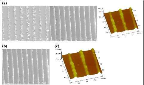
Dramatic changes in the pattern morphology were ob-served following high-temperature annealing applied to induce grain growth of the sapphire. Figure 4a shows a SEM image of the morphology of the patterned surface after annealing for 24 h at 450°C and 1 h at 1,200°C. For nanopatterned Al thin films that subsequently ex-perienced an annealing temperature of 1,200°C, it was found that smoothing and coalescence of the line fea-tures had occurred to such an extent that the patterning
[image:4.595.60.540.90.314.2]was no longer discernible. The phenomenon of surface diffusion-driven smoothing of surface features is well established in the literature [19-22] and occurs due to surface energy considerations [23,24]. The kinetics of the smoothing of the line patterns can be used to derive information on the diffusion mechanism. Therefore, for the successful fabrication of NPSS, the relative kinetics of smoothing versus grain growth of the underlying sap-phire is critical. Fortunately, for high-temperature an-nealing at 1,000°C and 1,100°C, the patterns were retained on sapphire substrates. Figure 4b shows a SEM image of the morphology of the patterned surface after high-temperature annealing for 1 h at 1,000°C. Figure 4c shows the AFM image of nanopatterned Al thin films with 250-nm-wide lines separated by 550-nm space after Figure 2Schematic illustration of soft PDMS mold based on quartz master mold.
Figure 3SEM images of the morphology of PDMS soft mold molding.From the quartz master (a), patterned AMONIL-MMS4 (b), and patterned Al thin films obtained by the UV-NIL and RIE (c).
Cuiet al. Nanoscale Research Letters2013,8:472 Page 4 of 6
[image:4.595.61.539.576.703.2]dual-stage annealing for 24 h at 450°C and 1 h at 1,000°C. Using this technique, it can be seen that the upper sur-faces of the patterns are not flat; instead, the center of the patterns is higher than the edges. Moreover, the height of the patterns following the high-temperature annealing of 1 h at 1,000°C was approximately150 nm. Our experi-mental results reveal that the consistency of line pat-terns fabricated by dual-stage annealing of patterned Al thin films for 24 h at 450°C and 1 h at 1,000°C and the orientation were the same as those of the sapphire (0001) substrates [14].
Therefore, it is believed that the above process has po-tential for the large-scale fabrication of NPSS for high output power GaN-based light-emitting diodes.
Conclusions
In this study, large-scale NPSS were fabricated by dual-stage annealing of patterned Al thin films prepared by soft UV-NIL and RIE. The soft mold with 550-nm-wide lines separated by 250-nm space was composed of the toluene-diluted PDMS layer supported by the soft
PDMS. The nanoimprint pressure is 3 × 10⁴Pa, and the
hold time of UV exposure is 90 s. Patterned Al thin films were subsequently subjected to dual-stage annealing. The first comprised a low-temperature oxidation anneal, where the annealing temperature was 450°C for 24 h.
This was followed by a high-temperature annealing in the range of 1,000°C to 1,200°C for 1 h to induce growth of the underlying sapphire single crystal to consume the oxide layer. The SEM results indicate that the patterns were retained on sapphire substrates after high-temperature annealing at less than 1,200°C. Finally, large-scale nanopatterned sapphire substrates were suc-cessfully fabricated by annealing of patterned Al thin films for 24 h at 450°C and 1 h at 1,000°C by soft UV-nanoimprint lithography. It is believed that the above process has potential for the large-scale fabrication of NPSS for high output power GaN-based light-emitting diodes.
Competing interests
The authors declare that they have no competing interests.
Authors' contributions
LC fabricated the large-scale nanopatterned sapphire substrates by annealing of patterned Al thin films by soft UV-nanoimprint lithography, analyzed the results, and wrote and revised the manuscript. J-CH, G-GW, and HYZ participated in the revision of the manuscript. RS and L-HL participated in the preparation of Al thin films. All authors read and approved the final manuscript.
Acknowledgements
[image:5.595.57.540.91.375.2]This project was supported by the National Natural Science Foundation of China (grant no.50902028), the Natural Science Foundation of Guangdong Province (grant no. 9451805707003351), the Weapon & Equipment Pre-research Foundation of General Armament Department (grant no.
9140A12050213HT01175), the Basic Research Plan Program of Shenzhen City in 2012 (grant no. JCYJ20120613134210982), and the Natural Scientific Research Innovation Foundation in Harbin Institute of Technology (grant no. HIT. NSFIR.2011123).
Author details
1Shenzhen Graduate School, Harbin Institute of Technology, Shenzhen 518055, People's Republic of China.2Center for Composite Materials, Harbin Institute of Technology, Harbin 150080, People's Republic of China.
Received: 4 July 2013 Accepted: 10 October 2013 Published: 11 November 2013
References
1. Schubert EF:Light-Emitting Diodes.Cambridge: Cambridge University Press; 2003:19–20.
2. Usui A, Sunakawa H, Sakai A, Yamaguchi AA:Thick GaN epitaxial growth with low dislocation density by hydride vapor phase epitaxy.Jpn J Appl Phys1997,36:L899–L902.
3. Iwaya M, Takeuchi T, Yamaguchi S, Wetzel C, Amano H, Akasaki I:Reduction of etch pit density in organometallic vapor phase epitaxy-grown GaN on sapphire by insertion of a low-temperature-deposited buffer layer between high-temperature-grown GaN.Jpn J Appl Phys1998,37:L316–L318. 4. Huh C, Lee KS, Kang EJ, Park SJ:Improved light-output and electrical
performance of InGaN-based light-emitting diode by microroughening of the p-GaN surface.J Appl Phys2003,93:9383–9385.
5. Yamada M, Mitani T, Narukawa Y, Shioji S, Niki I, Sonobe S, Deguchi K, Sano M, Mukai T:InGaN-based near-ultraviolet and blue-light-emitting diodes with high external quantum efficiency using a patterned sapphire substrate and a mesh electrode.Jpn J Appl Phys2002,41:L1431–L1433. 6. Feng ZH, Lau KM:Enhanced luminescence from GaN-based blue LEDs grown on grooved sapphire substrates.IEEE Photon Technol Lett2005,
17:1812–1814.
7. Li Z, Jiang Y, Yu T, Yang Z, Tao Y, Jia C, Chen Z, Yang Z, Zhang G:Analyses of surface temperatures on patterned sapphire substrate for the growth of GaN with metal organic chemical vapor deposition.Appl Surf Sci2011,
257:8062–8066.
8. Gao H, Yan F, Zhang Y, Li J, Zeng Y, Wang G:Fabrication of nano-patterned sapphire substrates and their application to the improvement of the performance of GaN-based LEDs.J Phys D Appl Phys2008,
41:115106-1–115106-5.
9. Hersee SD, Zubia D, Sun X, Bommena R, Fairchild M, Zhang S, Burckel D, Frauenglass A, Brueck SRJ:Nanoheteroepitaxy for the integration of highly mismatched semiconductor materials.IEEE J Quantum Electron
2002,38:1017–1028.
10. Zang KY, Wang YD, Chuaa SJ, Wang LS:Nanoscale lateral epitaxial overgrowth of GaN on Si (111).Appl Phys Lett2005,87:193106-1–193106-3. 11. Nakamura S, Mukai T, Senoh M:Candela-class high-brightness InGaN/
AlGaN double-heterostructure blue-light-emitting diodes.Appl Phys Lett
1994,64:1687–1689.
12. Yan F, Gao H, Zhang Y, Li J, Zeng Y, Wang G, Yang F:High-efficiency GaN-based blue LEDs grown on nano-patterned sapphire substrates for solid-state lighting.Proc SPIE2007,6841:684103-1–684103-7.
13. Park H, Chan HM, Vinci RP:Patterning of sapphire substrates via a solid state conversion process.J Mater Res2005,20:417–423.
14. Cui L, Wang G-G, Zhang H-Y, Han J-C:Effect of exposure parameters and annealing on the structure and morphological properties of nanopat-terned sapphire substrates prepared by solid state reaction.Ceram Int
2013. doi:10.1016/j.ceramint.2013.09.016.
15. Luo G, Maximov I, Adolph D, Graczyk M, Carlberg P, Ghatnekar-Nilsson S, Hessman D, Zhu T, Liu ZF, Xu HQ, Montelius L:Nanoimprint lithography for the fabrication of interdigitated cantilever arrays.Nanotechnol2006,
17:1906–1910.
16. Glinsner T, Plachetka U, Matthias T, Wimplinger M, Lindner P:Soft UV-based nanoimprint lithography for large-area imprinting applications.Proc SPIE
2007,6517:651718-1–651718-7.
17. Koo N, Plachetka U, Otto M, Bolten J, Heong J, Lee ES, Kurz H:Improved mold fabrication for the definition of high quality nanopatterns by soft UV-nanoimprint lithography using diluted PDMS material.
Microelectron Eng2007,84:904–908.
18. Ericson F, Kristensen N, Schweitz J:A transmission electron microscopy study of hillocks in thin aluminum films.J Vac Sci Technol B1991,9:58–63. 19. Maruyama T, Komatsu W:Surface diffusion of single-crystal Al2O3by
scratch-smoothing method.J Am Ceram Soc1975,58:338–339. 20. Bennison SJ, Harmer MP:Diffusion in sapphire and the role of magnesia
in the sintering of alumina.J Am Ceram Soc1990,73:833–837.
21. Glaeser AM:Ceramic Interfaces: Properties and Applications.London: Institute of Materials; 1998:241.
22. Bonzel HP:Surface morphologies: transient and equilibrium shapes.
Interface Sci2001,9:21–34.
23. Mullins WW:Flattening of a nearly plane solid surface due to capillarity.J Appl Phys1959,30:77–83.
24. Bonzel HP, Mullins WW:Smoothing of perturbed vicinal surfaces.Surf Sci
1996,350:285–300.
doi:10.1186/1556-276X-8-472
Cite this article as:Cuiet al.:Large-scale fabrication of nanopatterned
sapphire substrates by annealing of patterned Al thin films by soft UV-nanoimprint lithography.Nanoscale Research Letters20138:472.
Submit your manuscript to a
journal and benefi t from:
7Convenient online submission
7Rigorous peer review
7Immediate publication on acceptance
7Open access: articles freely available online
7High visibility within the fi eld
7Retaining the copyright to your article
Submit your next manuscript at 7 springeropen.com
Cuiet al. Nanoscale Research Letters2013,8:472 Page 6 of 6