N A N O E X P R E S S
Open Access
Dielectric properties of porous silicon for use
as a substrate for the on-chip integration of
millimeter-wave devices in the frequency range
140 to 210 GHz
Panagiotis Sarafis and Androula Galiouna Nassiopoulou
*Abstract
In this work, the dielectric properties of porous Si for its use as a local substrate material for the integration on the Si wafer of millimeter-wave devices were investigated in the frequency range 140 to 210 GHz. Broadband electrical characterization of coplanar waveguide transmission lines (CPW TLines), formed on the porous Si layer, was used in this respect. It was shown that the dielectric parameters of porous Si (dielectric permittivity and loss tangent) in the above frequency range have values similar to those obtained at lower frequencies (1 to 40 GHz). More specifically, for the samples used, the obtained values were approximately 3.12 ± 0.05 and 0.023 ± 0.005, respectively. Finally, a comparison was made between the performance of the CPW TLines on a 150-μm-thick porous Si layer and on three other radiofrequency (RF) substrates, namely, on trap-rich high-resistivity Si (trap-rich HR Si), on a standard complementary metal-oxide-semiconductor (CMOS) Si wafer (p-type, resistivity 1 to 10Ω.cm) and on quartz.
Keywords:Porous Si; Nanoscale semiconductors; RF characterization; Dielectric permittivity; Millimeter-wave passive devices
PACS:84.40.-x; 77.22.Ch; 81.05.Rm
Background
The co-integration of radiofrequency (RF) and millimeter-wave passive devices with complementary metal-oxide-semiconductor (CMOS) circuitry is quite challenging due to the low resistivity of the CMOS Si substrate that introduces important losses during electromagnetic wave propagation (eddy currents into the substrate). Another drawback towards this integration is the high permittivity of Si (εr,Si= 11.7) that causes an increase in crosstalk between lines, a decrease in antenna efficiency, and a reduction of the frequency of operation of the inductors. A viable solution recently investigated towards this inte-gration is the formation of a local substrate with the ap-propriate dielectric properties on the Si wafer, on which the RF and millimeter-wave devices will be integrated. Such a substrate is a thick porous Si layer with high
porosity, which can be optimized for best device perform-ance by choosing the appropriate layer thickness, in order to minimize electromagnetic propagation losses into Si, and the appropriate low values of the dielectric permittiv-ity, εr, and loss tangent. These last values are tunable by changing the material structure and morphology [1-6].
Porous Si structure (pore size, inter-pore distance) and morphology affect all its macroscopic properties (elec-trical, mechanical, optical, etc.) [7]. An intensive effort was made in the literature to correlate the electrical properties of the material with its structural parameters [8-12]. In view of the application of porous Si for the on-chip integration of RF and millimeter-wave devices, its dielectric properties (dielectric permittivity and loss tangent) as a function of frequency should be known, in order to be used by the device designer for an accurate prediction of device operation. In addition, since the di-electric properties of the material depend strongly on its structure and morphology [13], it is desirable to have an * Correspondence:[email protected]
NCSR Demokritos, INN, Terma Patriarchou Grigoriou, Aghia Paraskevi, 15310 Athens, Greece
experimental method to extract the dielectric parameters of the specific material used in each application.
In this work, we will first discuss the existing models that correlate the structural properties of porous Si (por-osity and morphology) with its dielectric properties and we will compare them with results obtained by a broad-band extraction method, based on the measurement of the S-parameters of coplanar waveguide transmission lines (CPW TLines) integrated on the porous Si sub-strate. By combining these measurements with electro-magnetic simulations, the dielectric permittivity and loss tangent of the substrate (porous Si) can be obtained. This method has been previously used by the authors to extract the dielectric parameters of porous Si in the frequency range 1 to 40 GHz [13,14]. In this work, mea-surements are extended to the frequency range 140 to 210 GHz. Finally, by comparing the performance of CPW TLines on porous Si and three other substrates used in RF, namely, a trap-rich high-resistivity (HR) Si substrate [15-17], a standard CMOS Si wafer (p-type, re-sistivity 1 to 10Ω.cm), and a quartz substrate, we dem-onstrate the superiority of porous Si as a local substrate for RF and millimeter-wave on-chip device integration.
Methods
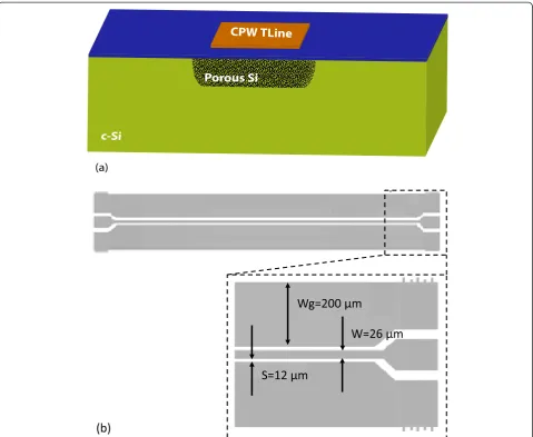
Fabrication of CPW TLines on porous Si layers
Thick PSi layers (thickness ~150μm) were formed by
an-odization of highly doped p-type Si (ρ= 1 to 5 mΩ.cm). The electrolytic solution was a mixture of HF and ethanol (3 EtOH(99.9%)/2 HF(50%) v.v.) and the anodization current density was J= 20 mA/cm2. The resulting layer
had a porosity of 76% and a dendritic structure as pre-sented in Figure 1. The porous Si layer was capped with 500 nm SiO2in order to stabilize it over time and achieve
better planarization of the porous Si surface for further processing. On top of PSi, covered by SiO2, a set of
copla-nar waveguide transmission lines (CPW TLines), made of 1-μm-thick patterned Al, was integrated (see Figure 2).
For comparison, identical CPW TLines were also fab-ricated on three other substrates, as follows: the first was the state-of-the-art trap-rich high-resistivity (HR) Si RF substrate [15]. This substrate was an n-type HR-Si wafer with nominal resistivity higher than 10 kΩ.cm, covered by a bilayer of a 500-nm-thick trap-rich poly-Si layer, deposited by low-pressure chemical vapor deposition
(LPCVD) at 625°C, and a-500 nm-thick TEOS SiO2
layer. The trap-rich layer is used to minimize the para-sitic surface conduction within the Si layer underneath the silicon oxide by trapping the parasitic charges and thus restoring the initial high resistivity of the Si sub-strate [17]. The second subsub-strate was a 380-μm-thick standard Si wafer used in CMOS-integrated circuits (ICs) (p-type, resistivity 1 to 10 Ω.cm). Finally, the last substrate was a 500-μm-thick quartz substrate, which is one of the off-chip RF substrates with almost negligible losses. This last substrate was used for comparison with the three other Si-based substrates.
RF measurements and de-embedding
[image:2.595.57.537.473.704.2]The S-parameters of the CPW TLines were measured in the 140-to-210-GHz range with an HP 8510B vector network analyzer (VNA) from Agilent (Santa Clara, CA,
Figure 1SEM image of highly porous Si.SEM image of highly porous Si formed on p+Si with resistivity 1 to 5 mΩ.cm. It depicts the vertical
USA), combined with a millimeter-wave VNA extension module by Oleson Microwave Labs (Morgan Hill, CA, USA). All the measurements were calibrated using the Line-Reflect-Reflect-Match (LRRM) algorithm of the Win-Cal software from Cascade Microtech (Beaverton, OR, USA). A de-embedding procedure is always necessary in order to decouple the device response from the parasitics due to the contacts and pads. The method followed was the two-line method, using the measured S-parameters of
two lines with different length (8 mm and 500 μm) [18].
The characteristic impedance, the propagation constant, and the effective permittivity of the lines were extracted and used to derive the dielectric parameters of the PSi substrate [13,14].
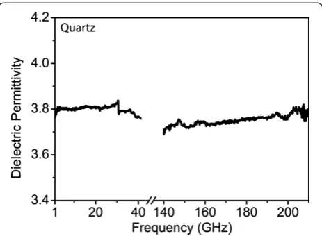
The de-embedding and the extraction method were first tested for the quartz substrate (fused silica), which is known to have a constant dielectric permittivity of 3.82
throughout the whole frequency range 1 to 210 GHz [19,20]. The extraction method is described in detail in [13]. The obtained results are depicted in Figure 3 for the frequency ranges 1 to 40 GHz and 140 to 210 GHz. We can see that the curves show continuity between the two frequency ranges and the extracted values of the permit-tivity are 3.82 for frequencies in the range 1 to 40 GHz and 3.71 to 3.79 for frequencies in the range 140 to 210 GHz. These results are very close to the literature value of quartz permittivity (3.82) and give confidence that the de-embedding and the parameter extraction methods are valid. They were thus used to characterize the porous Si layer in the above frequency ranges.
[image:3.595.59.539.88.481.2]Microscopic models for determining PSi dielectric properties Porous Si structure and morphology depend on the elec-trochemical conditions used for its formation as well as
on the starting wafer resistivity. Its dielectric properties are highly dependent on its structure and morphology. There are several works in the literature that correlate the material structure with its dielectric properties. Ac-cording to [9,21,22], the ac electrical transport of porous Si follows two mechanisms. The first is limited by the length of the carrier random walk through the fractal structure of the material and is valid in the very low fre-quency range, while at higher frequencies, the random path is shorter and the hopping length stops to be the critical factor. In that case, conduction is mainly deter-mined by the distance between inhomogeneous areas [22]. The dielectric permittivity of porous Si (εPSi) de-scribes the polarization of the atoms and the impurities inside the material. As it is shown in [22], εPSidepends on frequency only for frequencies <100 Hz. For higher frequencies, its value is saturated and remains constant up to at least 100 kHz. This value is also independent of temperature.
Effective medium approximation
Instead of considering carrier transport at the nanoscale, it is easier to correlate the dielectric properties of the material with macroscopic parameters, as for example the material porosity. An effective medium approxima-tion (EMA) is used in this respect. This approximaapproxima-tion is valid when the wavelength of the signal is much larger than the typical dimensions of pores and nanostructures composing the material. The most common models used
in the literature to correlate the permittivity of non-oxidized porous Si with its porosity are the following:
Vegard’s approximation[1]
Vegard’s approximation is a simple mixing model correlating the dielectric permittivity with porosity (P) through the relation:
εPSi ¼Pεairþð1−PÞεSi; ð1Þ
whereεPSiis the permittivity of porous Si,εairis the permittivity of air, andεSiis the permittivity of Si and P is the porosity.
Maxwell-Garnett’s approximation[23]
This is valid for systems in which the filling fractionf
(wheref= 1−P) of the porous material is far smaller than the porosity (P) [23]. The following expression is obtained:
εPSi−εair εPSiþ2εair ¼
1−P
ð Þ εSi−εair
εSiþ2εair ð
2Þ
Bruggeman’s approximation[23].
This is applied to structures where the filling fraction is comparable to the porosity [23]. The following expression relates the dielectric permittivity with the porosity:
P εPSi−εair
εPSiþ2εair¼ 1−P
ð Þ εSi−εair
εSiþ2εair ð
3Þ
Bergman’s approximation[24]
It introduces the spectral density functiong(n,P)to take into account the nanotopology of the material. The following expression is obtained:
εPSi ¼εair 1−f
Z1
0
g nð ;fÞ
εair εair−εSi−n
dn 0
@
1
A ð4Þ
From all the above models, Vegard’s approximation is the simplest one. The most commonly used model is the Bruggeman’s model [11,25]. Both the Vegard’s model for
non-oxidized Si and the Maxwell-Garnett’s model have
been proven to be insufficient to explain the results of several experiments [13,24,26]. An improved version of
the Vegard’s model incorporates also the SiO2 native
[image:4.595.58.290.88.258.2]oxide surrounding the Si nanostructures composing the material [27]. Better agreement between the model and experimental results is obtained in this case. The oxida-tion of the Si skeleton leads to a decreased permittivity of the material [11,27]. This is because the oxidation not only changes material composition, but also leads to reduction of material porosity. Finally, the Bergman’s approximation predicts quite well the dielectric behavior of PSi in the optical frequencies. The spectral density
function g(n,f)that describes the micro-topology of the material has to be extracted in this respect [12].
Dielectric parameter extraction using broadband electrical measurements
The models of Vegard, Maxwell-Garnett, and Bruggeman,
as presented above, relate εPSi with material porosity.
However, they were insufficient to explain the experimen-tal results of several groups [13,26,28]. This can be attrib-uted to the complexity of the PSi structure and morphology, which differs from one sample to another, even if the macroscopic porosity is the same. It is also quite difficult to find a representativeg(n,f)function that accurately describes the specific porous Si structure and
morphology in each case, making the Bergman’s model
difficult to use. It is thus interesting to have a method to characterize the specific PSi material used in each experi-ment by simply measuring the electromagnetic (EM) re-sponse of a device integrated on it. This is the approach we use in this work. By integrating CPW TLines on top of porous Si and measuring their S-parameters, we extract porous Si dielectric parameters by combining the experi-mental results with electromagnetic simulations and con-formal mapping calculations. This method has been described in detail in [13,14], and the results have been proven to be in very good agreement with full-wave EM simulations [14].
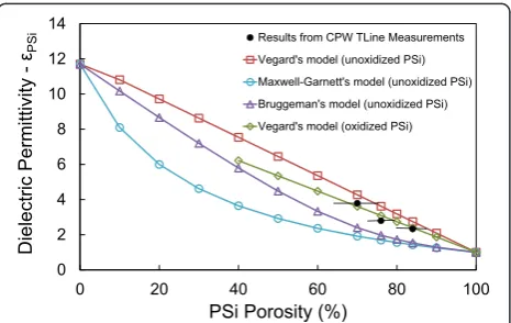
In Figure 4 the extracted dielectric permittivity of three PSi layers with 70%, 76%, and 84% porosity using the above method are depicted in full black circles. The
PSi layers were fabricated on a p+-type Si wafer with
resistivity 1 to 5 mΩ.cm and had a surface area of 4 cm2. Identical transmission lines were integrated on all three samples (see Figure 2b). The obtained results were
compared with those obtained using Vegard’s,
Maxwell-Garnett’s and Bruggeman’s models for PSi by applying formulas (1) to (3) given above. From Figure 4, it can be seen that the values of the extracted permittivity using broadband electrical measurements of the specific CPW TLines are between those obtained with the Bruggeman’s and Vegard’s models for non-oxidized PSi. On the other hand, by using the more elaborated Vegard’s law described in [27], which takes into account the presence of a native oxide shell surrounding the Si nanostructures (in our case, we considered a native oxide thickness of 1.5 nm and a Si skeleton thickness of 10 nm), better agreement is achieved between our experimental results and the calculated ones.
Results and discussion
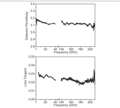
Porous Si dielectric parameters in the frequency range 140 to 210 GHz
Using broadband electrical measurements combined with simulations, the dielectric parameters of PSi in the frequency range 140 to 210 GHz were extracted. The obtained results are presented in Figure 5 in comparison with the extracted parameters for the frequency range 1 to 40 GHz. At low frequencies (1 to 40 GHz), there is an
initial slight monotonic decrease of εPSi from 3.19 to
3.12 and it then stabilizes around this value (Figure 5a).
In the high-frequency range (140 to 210 GHz), εPSi
oscillates around the values of 3.1 and 3.2, within a maximum deviation of 0.1. Similarly, the value of the loss tangent is between 0.031 and 0.023 in the range 5 to 40 GHz (see Figure 5b), while it stays constant at 0.023 in the range 140 to 210 GHz, with a maximum deviation of 0.005. In the 1-to-5-GHz range, the results are not reliable due to the contact resistance between the RF probes and the pads and were omitted. This effect becomes negli-gible at higher frequencies.
In overall, from the above, we can deduce that the di-electric permittivity of porous Si is almost constant in the studied frequency ranges. It also shows a continuity of the two curves, suggesting the same constant value in the frequency range 40 to 140 GHz. The loss tangent shows a slight decrease with frequency, while again there is continuity between the low- and high-frequency curves.
Comparison of PSi with other RF and millimeter-wave substrates
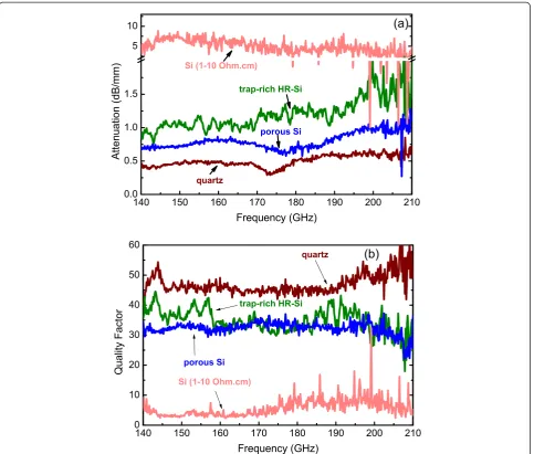
[image:5.595.58.291.498.645.2]In order to demonstrate the high performance of porous Si for use as a substrate for RF and millimeter-wave devices, a comparison was made between this substrate and three other substrates used in the same respect. Identical CPW TLines were integrated on the four dif-ferent substrates, their S-parameters were measured,
and the propagation constant for each line was ex-tracted. Figure 6 shows the extracted values of signal attenuation (a) and quality factor (b) for the CPW TLines on the four different substrates. We deduce that the lines on the three substrates, trap-rich HR Si, PSi, and quartz, have better performance than those on the low-resistivity CMOS Si. More specifically, trap-rich HR-Si reduces losses from 4.8 to 1.6 dB/mm at 210 GHz, while PSi leads to a further decrease of the attenuation loss of 1.2 dB/mm at 210 GHz. Both the above sub-strates show similar performance with quartz, which is a non-Si, off-chip substrate.
The observed reduction of signal attenuation a and
the increase of the quality factor Q of the CPW TLine
on PSi versus bulk Si is attributed to the reduction of the material loss tangent and dielectric permittivity through nanostructuring. As shown previously by the authors, the achieved low permittivity of porous Si at high porosities shows advantages in many RF and millimeter-wave devices, namely, high-characteristic im-pedance of the CPW TLines [5], inductors operating at higher frequencies [29,30] and antennas with reduced surface waves induced into the substrate can be obtained.
Conclusions
[image:6.595.60.538.86.515.2]The dielectric properties of a 150-μm-thick PSi layer with 76% porosity were presented for the first time for
the frequency range 140 to 210 GHz, using broadband electrical measurements combined with electromagnetic simulations. It was found that the dielectric permittivity is almost constant in the above frequency range, having approximately the same value as at lower frequencies. The loss tangent is also almost constant with fre-quency. Finally, a comparison between the performance of CPW TLines on PSi, trap-rich HR Si, quartz, and standard low-resistivity CMOS Si was made in the above frequency range. An almost equal performance was obtained between the trap-rich HR Si, PSi, and quartz. At 210 GHz, porous Si showed an attenuation as low as 1 dB/mm and the quality factor was ~30. This performance is added to the other advantages of PSi compared to other Si-based substrates, e.g., its
compatibility with the low-resistivity CMOS substrate (permitting co-integration of CMOS logic with RF and millimeter-wave devices on the same substrate) and its low achievable permittivity). All the above make PSi an excellent local substrate on the Si wafer for RF and millimeter-wave device integration on the Si chip, pav-ing the way towards the digital/RF analog system-on-chip (SoC) of the future.
Competing interests
The authors declare that they have no competing interests.
Authors’contributions
[image:7.595.58.542.88.499.2]PS made the experiments and drafted the paper, while AGN supervised the work and revised the paper. Both authors read and approved the final manuscript.
Acknowledgements
The trap-rich high-resistivity Si wafers were provided by UCL Belgium (Jean-Pierre Raskin), while measurements in the frequency range 140 to 210 GHz of the CPW TLines were conducted in the facilities of VTT, Helsinki, Finland (arranged by A. Markus) during a visit of P. Sarafis to VTT. This work was supported by the EU Network of Excellence‘Nanofunction’through the EU 7th Framework Programme for Research under Contract 257375.
Received: 9 May 2014 Accepted: 15 July 2014 Published: 21 August 2014
References
1. Kim H-S, Xie Y-H, DeVincentis M, Itoh T, Jenkins K a:Unoxidized porous Si as an isolation material for mixed-signal integrated circuit applications.
J Appl Phys2003,93:4226.
2. Welty R, Park S, Asbeck PM, Dancil K-PS, Sailor MJ:Porous silicon technology for RF integrated circuit applications. In1998 Top. Meet. Silicon Monolith. Integr. Circuits RF Syst. Dig. Pap. (Cat. No.98EX271).IEEE; 1998:160–163. 3. Gautier G, Leduc P:Porous silicon for electrical isolation in radio
frequency devices: a review.Appl Phys Rev2014,1:011101.
4. Capelle M, Billoué J, Poveda P, Gautier G:RF performances of inductors integrated on localized p + -type porous silicon regions.Nanoscale Res Lett2012,7:523.
5. Issa H, Ferrari P, Hourdakis E, Nassiopoulou AG:On-chip high-performance millimeter-wave transmission lines on locally grown porous silicon areas.
IEEE Trans Electron Devices2011,58:3720–3724.
6. Capelle M, Billoué J, Poveda P, Gautier G:Study of porous silicon substrates for the monolithic integration of radiofrequency circuits.Int J Microw Wirel Technol2013,6:39–43.
7. “Properties of porous silicon”Emis Datareviews. Ser. No18, IEE, an INSPEC Publ. UK, edited by L.T.Canham. 1997.1997.
8. Di Francia G, La Ferrara V, Maddalena P, Ninno D, Odierna LP, Cataudella V:
AC conductivity of porous silicon: a fractal and surface transport mechanism.Il Nuovo Cimento D1996,18:1187–1196.
9. Lehmann V, Hofmann F, Möller F, Grüning U:Resistivity of porous silicon: a surface effect.Thin Solid Films1995,255:20–22.
10. Boarino L, Borini S, Amato G:Electrical properties of mesoporous silicon: from a surface effect to coulomb blockade and more.J Electrochem Soc
2009,156:K223.
11. Astrova E, Tolmachev V:Effective refractive index and composition of oxidized porous silicon films.Mater Sci Eng B2000,69–70:142–148. 12. TheiβW:The dielectric function of porous silicon - how to obtain it and
how to use it.Thin Solid Films1996,276:7–12.
13. Sarafis P, Hourdakis E, Nassiopoulou AG:Dielectric permittivity of Porous Si for use as substrate material in Si-integrated RF devices.IEEE Trans Electron Devices2013,60:1436–1443.
14. Sarafis P, Hourdakis E, Nassiopoulou AG:Porous Si dielectric parameter extraction for use in RF passive device integration : Measurements and simulations. In43rd Eur. Solid-State Device Res. Conf. Bucharest.2013:99–102. 15. Neve CR, Ben Alia K, Malaquin C, Allibert F, Desbonnets E, Bertrand I, Van
Den Daele W, Raskin J-P:RF and linear performance of commercial 200 mm trap-rich HR-SOI wafers for SoC applications. In2013 IEEE 13th Top. Meet. Silicon Monolith. Integr. Circuits RF Syst.Austin, TX, USA: IEEE; 2013:15–17. 16. Ben AK, Neve CR, Gharsallah A, Raskin J:RF performance of SOI CMOS
technology on commercial 200-mm enhanced signal integrity high resistivity SOI substrate.IEEE Trans Electron Devices2014,61:722–728. 17. Lederer D, Raskin J-P:Effective resistivity of fully-processed SOI substrates.
Solid State Electron2005,49:491–496.
18. Mangan AM, Voinigescu SP, Tazlauanu M:De-embedding transmission line measurements for accurate modeling of IC designs.IEEE Trans Electron Devices2006,53:235–241.
19. Lamb JW:Miscellaneous data on materials for millimetre and submillimetre optics.Int J Infrared Millimeter Waves1996,17:1997–2034. 20. Cheng H-J, Whitaker JF, Weller TM, Katehi LPB:Terahertz-bandwidth
characteristics of coplanar transmission lines on low permittivity substrates.IEEE Trans Microw Theory Tech1994,42:2399–2406. 21. Ben-Chorin M, Möller F, Koch F:Nonlinear electrical transport in porous
silicon.Phys Rev B1994,49:2981–2984.
22. Ben-Chorin M, Möller F, Koch F, Schirmacher W, Eberhard M:Hopping transport on a fractal: ac conductivity of porous silicon.Phys Rev B1995,
51:2199–2213.
23. Campos AM, Torres J, Giraldo JJ:Porous silicon dielectric function modeling from effective medium theories.Surf Rev Lett2002,
09:1631–1635.
24. TheiβW, Henkel S, Arntzen M:Connecting microscopic and macroscopic properties of porous media: choosing appropriate effective medium concepts.Thin Solid Films1995,255:177–180.
25. Khardani M, Bouaïcha M, Bessaïs B:Bruggeman effective medium approach for modelling optical properties of porous silicon: comparison with experiment.Phys Status Solidi2007,4:1986–1990.
26. Ramani S, Cheville A, Escorcia Garcia J, Agarwal V:Conductivity of free-standing porous silicon layers using Terahertz differential time-domain spectroscopy.Phys Status Solidi2007,4:2111–2115.
27. Theodoropoulou M, Pagonis DN, Nassiopoulou AG, Krontiras CA, Georga SN:
Dielectric characterization of macroporous thick silicon films in the frequency range 1 Hz-1 MHz.Phys Status Solidi2008,5:3597–3600. 28. Menard S, Fevre A, Capelle M, Defforge T, Billoue J, Gautier G:Dielectric
behaviour of porous silicon grown from p-type substrates. InInt. Conf. Porous Semicond. - Sci. Technol, 0.Benidorm-Alicante: 2014:122–123. 29. Sarafis P, Hourdakis E, Nassiopoulou AG, Roda Neve C, Ben Ali K, Raskin J-P:
Advanced Si-based substrates for RF passive integration: comparison between local porous Si layer technology and trap-rich high resistivity Si.Solid State Electron2013,87:27–33.
30. Capelle M, Billoue J, Poveda P, Gautier G:N-type porous silicon substrates for integrated RF inductors.IEEE Trans Electron Devices2011,58:4111–4114.
doi:10.1186/1556-276X-9-418
Cite this article as:Sarafis and Nassiopoulou:Dielectric properties of porous silicon for use as a substrate for the on-chip integration of millimeter-wave devices in the frequency range 140 to 210 GHz.
Nanoscale Research Letters20149:418.
Submit your manuscript to a
journal and benefi t from:
7Convenient online submission 7Rigorous peer review
7Immediate publication on acceptance 7Open access: articles freely available online 7High visibility within the fi eld
7Retaining the copyright to your article