N A N O R E V I E W
Open Access
Ferroelectric memory based on nanostructures
Xingqiang Liu
1, Yueli Liu
2, Wen Chen
2, Jinchai Li
1and Lei Liao
1*Abstract:In the past decades, ferroelectric materials have attracted wide attention due to their applications in nonvolatile memory devices (NVMDs) rendered by the electrically switchable spontaneous polarizations. Furthermore, the combination of ferroelectric and nanomaterials opens a new route to fabricating a nanoscale memory device with ultrahigh memory integration, which greatly eases the ever increasing scaling and economic challenges encountered in the traditional semiconductor industry. In this review, we summarize the recent
development of the nonvolatile ferroelectric field effect transistor (FeFET) memory devices based on nanostructures. The operating principles of FeFET are introduced first, followed by the discussion of the real FeFET memory
nanodevices based on oxide nanowires, nanoparticles, semiconductor nanotetrapods, carbon nanotubes, and graphene. Finally, we present the opportunities and challenges in nanomemory devices and our views on the future prospects of NVMDs.
Introduction
According to Moore's law, the number of transistors accommodated on the integrated circuits doubles roughly every 18 months and so does the performance [1]. As the essential part of the integrated circuits, non-volatile memory devices (NVMDs) have been heavily deployed in portable electronic devices to realize secure and fast data transfer, such as the ID cards, MP3 player, and so on. The versatile NVMDs should be reprogram-mable and require a mechanism of repeatable switching between different binary states [2-4]. The ferroelectric field effect transistor (FeFET) is one of such promising NVMDs with the lowest power consumption [5] and high speed bearing comparable to that of dynamic ran-dom access memory [6]. Other memory mechanisms in-cluding polarization induced by the polar molecule (such as H2O) adsorption/desorption and by the defect-related charge-trapping layer have also been studied [7-9]. However, both the adsorption/desorption and the defect-related charge-trapping mechanisms suffer from reproducibility problems caused by the nature that nei-ther the adsorption/desorption of polar molecules nor the amount or distribution of the defects can be exactly controlled, which creates a great challenge for reproduction. This review therefore gives an overview of
the advances of FeFET for NVMDs in the current state and the future.
The simple architectural structures and mature fabrica-tion technologies of the tradifabrica-tional thin-film transistor have sparked a surge of interest in the thin-film FeFET for NVMDs. However, theoretical calculation has shown that the planar corrugations effectively worsen the distribution of polarization bound charges [10], due to smearing of the phase transition. It's well recognized that the physical properties of ferroelectric thin film are significantly limited by a critical size [11-13]. Furthermore, with the decrease in the thickness of the ferroelectric thin film, the remnant polarization (Pr) decreases and the coercive field (Ec) turns up increasingly due to the collapsed dielectric response [14-18]. This imposes a serious limitation on the desired integrated density and leads to poor performance in the thin-film transistor-based NVMDs [19]. In order to fulfill the particularly required performance such as retention time, endurance, response time, and/or power consump-tion, plenty of nanomaterials and alternative technologies have been utilized to enhance the integrated density and performance, which open a route to overcome the scaling limitations and economic challenges encountered in the current silicon industry [20-24]. In this survey, we summarize the current researches on fabricating a promis-ing nano-FeFET. This paper is organized as follows: the ‘Ferroelectric and the operating principle of FeFET’section summarizes the structure and characters of ferroelectric and the operating principle of FeFET. The ‘Current researches’ section reviews the current state of nano-* Correspondence:[email protected]
1Key Laboratory of Artificial Micro- and Nano-structures of Ministry of
Education, and School of Physics and Technology, Wuhan University, Wuhan 430072, People's Republic of China
Full list of author information is available at the end of the article
FeFET devices, including the combinations of ferroelec-trics with nanowires (NWs) [17,25-28], nanoparticles (NPs) [29-32], three-dimensional (3D) nanostructures [33-35], carbon nanotubes (CNTs) [36-45], and graphene [43,46-49]. The ‘Challenges and improvements’ section explains the fatigue mechanism and provides an overview of the efforts that have been taken to improve the fatigue resistance. The‘Conclusions’section gives an outlook and conclusion for the practical applications of FeFET.
Ferroelectric and the operating principle of FeFET
The uniform characters of ferroelectrics offer opportunities for fabricating NVMDs. Devices based on one-dimensional (1D) [17,25,37-39] or two-dimensional (2D) [43,46] nanostructures have been realized with excellent per-formance [50,51]. This section is divided into two parts: Ferroelectric is introduced first followed by the
descriptions of the structure and principle of
polarization. The operating and programming princi-ples of FeFET for memory are then presented.
Ferroelectric
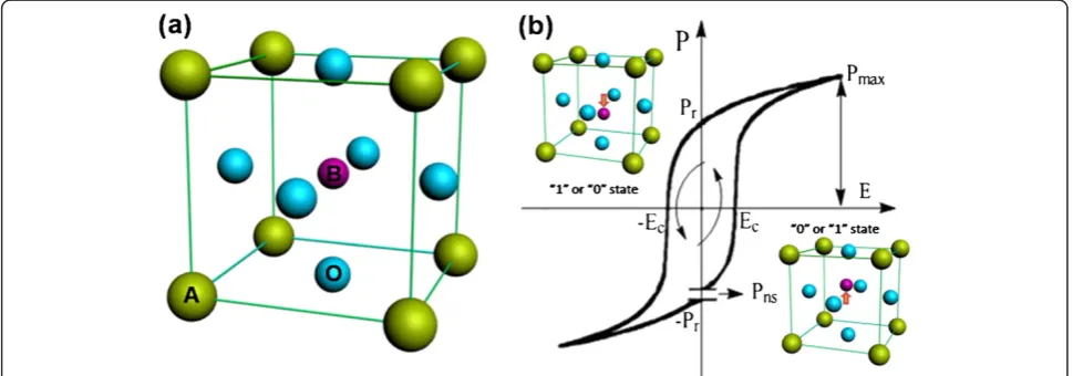
In general, ferroelectrics are dielectric crystals with the perovskite structure, [22] whose formula is ABO3 with the schematic structure shown in Figure 1a. The spon-taneous polarization arises as the temperature sweeps due to a lattice distortion which involves the relative dis-placements of B4+in each cell. These ferroelectric beha-viors appear only under an inherent temperature (Curie temperature TC). As shown in Figure 1b, the similar polarization phenomenon can also be exhibited from the ferroelectric under the condition of an external electric field (E), in which the intensity of polarization (P) does not exhibit a linear response to E but instead shows a
closed hysteretic loop. WhenEstrides a particular value, the polarization is reversed, and we call this value coer-cive field Ec (see Figure 1b). In other words, P can be
switched by modulating E, and the remnant
polarization +Pr and−Pr states are stored in ferroelec-tric. The bistable state of ferroelectric can be pro-grammed as binary information ‘1’ and ‘0’for NVMDs. Considerable efforts therefore have been taken to exploit available NVMD devices based on this.
FeFET
[image:2.595.56.541.512.682.2]A reasonable model is critical in order to take the advantages of ferroelectric for fabricating the NVMDs [52]. The typical memory devices are built on the base of the capacitor [5,53,54] or FeFET [55,56]. The former model consists of a thin ferroelectric film be-tween two conductive electrodes, and the latter one is similar to a metal-oxide-semiconductor field-effect transistor (MOSFET). Figure 2 shows the schematic diagrams of both. Shiga et al. have demonstrated that the signal significantly deteriorates as the capacitor size scales down, which limits the memory capacity to 128 Mb. [57]. The leakage current is another key challenge for the development of capacitor-based NVMDs [58]. On the other hand, FeFET has a well-defined memory switch behavior with simple nondes-tructive readout (NDRO) process carried out by detecting IDS or the resistance of the active channel. Due to the excellent performance obtained, the inte-gration of ferroelectrics with nanomaterials has been extensively explored in previous works [2,43,59-61], where ultimate scalability has been reported as well. Thus, in this paper, we give the special attention to FeFET-based memory devices with nanostructures.
Figure 1Schematic structure (a) and hysteresis loop curve of ferroelectric (b).In(a), the green balls represent the A2+, blue balls are O2−,
and the purple one is B4+; they are located at the vertex angle, centroid, and body center, respectively. In(b), the inserts are the corresponding
location of B4+in the lattice cell, with the bistability state obviously different from that of the dynamic random access memory which needs
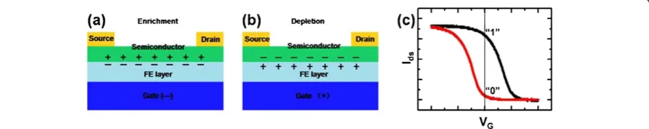
Unlike MOSFET, the oxide-gate dielectric is replaced by ferroelectric in FeFET. By modulating the gate bias, the carriers accumulate or deplete at the ferroelectric (FE)-semiconductor interface, leading the FeFET on or off, as shown in Figure 3a,b (a p-channel FeFET) [62]. The corresponding transfer curve of IDS versus VG has been depicted in Figure 3c. With the polarization of the FE layer, the curve of IDSvaries with VG as a hysteretic loop whenVGsweeps upward (from negative to positive) and then downward (from positive to negative) continu-ously. Moreover, even if VG is released, the charges re-main; thus, the device retains its state. Therefore, as VG= 0 V, the device still exhibits an on or off state, which can be defined as 1 and 0. In other words, the in-formation in FeFET is not lost even when encountering a power outage. The information can be read out by detecting theIDSor the resistance of the active channel. Figure 3c is the corresponding closed hysteretic loop of IDS versus VG, which shows the track of switching be-tween the 0 and 1 state. It's evident that the appropriate large value of Pr and low EC are important for the per-formance of FeFET [59,63]. A too low Pr may not be able to induce enough accumulated carriers at the FE-semiconductor interface to give rise to an evident change of conductance of the channel. On the other hand, although a lowECcan realize a low operating bias, it also raises a serious accompanying instability problem
since a low voltage is not enough to switch the states of the device, which can be solved by the concessive method using a thick FE layer. In general, the properties of ferroelectric are essential for the fabrication of FeFET.
Current researches
With the development of the fundamental material sci-ence, tremendous progress has been made to fabricate FeFET for NVMDs based on coetaneous advanced mate-rials. In this section, we discuss the current research on FeFET for NVMDs.
Oxide NW-based FeFET
[image:3.595.54.540.89.220.2]Based on the traditional thin-film FET, it is easy to fabri-cate a thin-film FeFET. Although its simple structure can supply easy fabrication [64], it also suffers from several problems which need to be solved [65,66]. For example, the EC of the film is typically several kilovolts per centimeter, which requires a high operating voltage to reverse the polarization. Moreover, the poor polarization value can hardly effect an evident conduct-ance change [67]. On top of these, the low field-effect mobility, low on/off ratio, low subthreshold slope, and the poor switch speed are limitations impacting the applications of the thin-film FeFET [68-70]. In recent years, oxide NWs have emerged as promising building blocks in various technological domains including Figure 2The current models of NVMDs.(a) The capacitor model, consisting of a thin ferroelectric film between two conductive electrodes. (b) The FeFET model, which replaces the dielectric of MOSFET with ferroelectric.
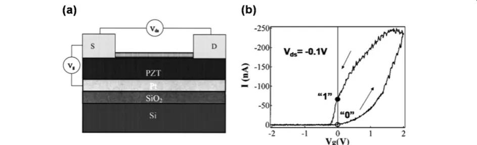
[image:3.595.65.538.610.704.2]fundamental researches and nanodevice applications due to their unique structures and stable properties [71,72]. Tremendous efforts have been made to fabricate NW FeFETs, which use the NWs as the active channel. In the early days, In2O3 NWs have been integrated with lead zirconate titanate (PZT) to fabricate FeFET. Due to the high dielectric constant and the switchable spontaneous polarization of PZT, the fabricated device received an enhanced performance and memory effect [25], when compared with the traditional SiO2-gate FET. The sche-matic diagram is shown in Figure 4a, which reveals that the back-gate FeFET structure has been used in this re-search. The In2O3NWs with a diameter of 10 nm were first ultrasonicated in isopropanol and then deposited onto the PZT/Pt/SiO2/Si substrate by spin-coating tech-nique. Photolithography, Ti/Au deposition, and lift off were carried out subsequently to pattern the source and drain electrodes, which were in contact with an individ-ual NW. The fabricated FeFET operated on an accumu-lation/depletion mode with the conduction of the active NW channel modulated by the gate potential. Figure 4b shows the transfer curves of the memory device, exhibit-ing a closed counterclockwise loop, whenVGwas sweep-ing upward and then downward. AsVG= 0 V, there were two pronouncedly different values of IDS, which were caused by the switchableProf the PZT layer. Hence, we could define the larger one as a binary 1 and the smaller one as 0 to realize the basic program function. More-over, the methods used in this experiment could be gen-eralized and applied to other NW systems to obtain nanoscale memory devices.
Having inherent defects in ZnO NWs, such as oxygen vacancies and Zn interstitials, ZnO NWs present the char-acter of the natural n-type semiconductor [73]. In Liao's recent work [2], ZnO NW was combined with PZT thin film to realize the memory function successfully. The schematic diagram and scanning electron microscopy (SEM) image were shown in Figure 5a,b, respectively. As
[image:4.595.306.539.87.353.2]ZnO NW is an n-type semiconductor, with the polarization of PZT, a positive pulse gate voltage would raise up the band of the channel and then deplete the elec-trons in the NW, as shown in Figure 5c. The device pre-sented an effectively‘off’state, which could be defined as a binary 0. The binary 1 representing the opposite state could be defined as well in Figure 5d. Based on this principle, the state of the device could be switched by a timely pulse; in other words, the programming process was realized. The transfer character also demonstrated the
[image:4.595.66.538.558.702.2]Figure 4Schematic circuit diagram of In2O3nanowire FeFET (a) and characteristics of PZT-gated In2O3NW transistor (b).The PZT-gated In2O3NW transistor withVDS=−0.1 V shows pronounced hysteresis.‘1’and‘0’denote two states atVG= 0 V for the memory operation.
switching mechanism with two pronounced states at VG= 0 V, which is shown in Figure 6a. Reading cycles of 103of both 1 and 0 states were carried out in Figure 6b. As we can see, the two states were still well distinguish-able, showing a sustaining memory performance.
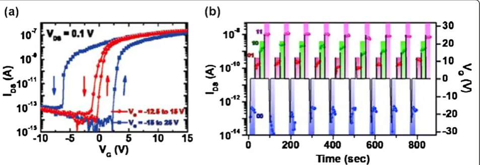
Despite the achievements made with the NWs, which yield many attractive features and desirable capability for potential applications, there are still many more new approaches coming up to further improve the integrated density. The multi-bit FeFET has been considered to supply higher density for storage, which could overcome the scaling limitations and economic challenges in the current silicon industry. The ZnO NW FET (Figure 7a) with coated ferroelectric BaTiO3(BTO) NPs has realized the function for a two-bit memory [17]. Figure 7b,c showed the schematic view of the differing degrees of reoriented electric dipole moments when a positive and negative bias was applied, respectively. The polarization of the NPs gave rise to a higher positive gate bias and then induced more polarized NPs. The more polarized charges were accumulated at the NP-NW interface, the larger the conductance of the active channel was. The surface engineering further caused a positive shift of the threshold voltage (Vth). In Figure 8a, it's obvious to find that Vthwas dependent on the sweep range of the gate voltage as well as the sweep direction. A more negative initial sweep voltage caused a more positive shift ofVth. Similarly, a more negative threshold voltage shift was related to a more positive initial sweep voltage. In addition, as mentioned previously, the information could be read out by detecting the current or the active chan-nel resistance, so an individual device used herein could store multi-bit information with different gate voltage pulses. The different states of the IDSwere correspond-ing to different binary information, which could be modulated by varying gate voltage pulses. Figure 8b showed the detailed practical process of programming
‘00’,‘01’,‘10’, and ‘11’ states. With the ability of storing multi-bit information in an individual memory device, the device reported herein provided a new way to en-hance the integrated density.
Furthermore, the synthesis methods applied here demonstrated a simple room-temperature process for in-tegrating the FE NPs with ZnO NW to fabricate the multi-bit memory device. The device fabricated in this way had a remarkably high on/off ratio of 104and a long retention time over 4 × 10⁴ s, which made it easy to recognize the two binary states. This work thus provided a viable route to fabricate high density NVMDs to over-come the existing physical and technological limitations.
Nanotetrapod-based FeFET
In order to exploit the bottom-up technology, extensive studies on 3D structure-based devices have flourished, inspired by the peculiar prosperity of the architectures. Depending on the kinetics of the growth process, two crystal structures of one same compound can exist sta-bly. Despite the changes in size, the additional structure provides more electronic states and characters. These special features provide the precious opportunity for making efficient nanodevices. CdS nanotetrapods pro-vide a typical example in which each individual
nanote-trapod is combined with the pyramidal-shaped
zincblende structure core and wurtzite arms, with the electrons and holes located in each other, respectively. Moreover, the bandgap of the arms is larger than the one of the core. With the type II band alignment, a pe-culiar electron transport is observed.
[image:5.595.58.540.553.695.2]Due to the unique and also discommodious 3D struc-ture, CdS nanotetrapods were impossible to lie flat on the gate, resulting in poor capacitance coupling, whereas the ferroelectric with high dielectric constant can make up it; therefore, the memory effect was also observed [35]. Figure 9a shows the schematic diagram, Figure 9b,c
Figure 6Memory characteristics ZnO NW FeFET device.(a)IDS-VGtransfer characteristics atVDS= 2 V of a FeFET device based on a ferroelectric
PZT gate oxide. (b) Endurance tests by measuring the off- and on-state drain current at a fixedVDS= 2 V as a function of programming cycles of the
shows the transmission electron microscopy (TEM) images of CdS nanotetrapods, and Figure 9d,e shows the SEM images of the device. To investigate the perform-ance of the prepared device, the transfer character of the device was measured with the gate voltage swept upward and then downward continually under various tempera-tures (see Table 1). It is obvious that a counterclockwise hysteretic loop is presented at 300 K, whereas a clock-wise hysteretic loop is presented at 80 K. The phenomenon in Figure 1a could be attributed to the ‘charge-store’memory effect [74]. The defects in the FE layer and the FE-CdS interface provided the low poten-tial site for storing charges which affects the distribution
[image:6.595.59.540.90.228.2]of the charges in the active channel, just like floating gates. On the other hand, the typical ferroelectric mem-ory clockwise loop in Figure 10b indicated that the ferroelectric memory played the dominant role at low temperature. The charge-store memory effect competed with ferroelectric memory as the temperature varied. This was demonstrated by the curve at 140K where no evident hysteretic loop was present (Figure 10c). At low temperature, few trapped charges were active, and the charge-store effect became frozen [75]; therefore, the ferroelectric memory effect became dominant, which was proved by the ferroelectric character at 8.5K (Figure 10d). The positive voltage led to−Pr in the FE
Figure 7Schematic views of ZnO NW FET and polarization model for FE NPs surrounding a NW.(a) A schematic view of a top-gate FET-based nonvolatile memory device. For a top-gate ZnO NW FET where a ZnO NW is incorporated with FE NPs, cross-linked poly (4-vinylphenol) (c-PVP) was used as a gate dielectric. (b,c) The schematic views of a simplified polarization model for FE NPs surrounding a NW. The lines show the electric field distribution between a ZnO NW and a gate electrode. Electric dipole moments are reoriented along electric field lines, resulting in different polarization states according to the gate electric field strength. Furthermore, affected by more reoriented electric dipole moments, the denser the equipotential lines around the upper part of a NW are, the easier it is to induce more polarized charges at the FE-NW interface. Thus, different conductance states result from different net amounts of reoriented electric dipole moments dependent on the applied gate electric field strength.
Figure 8Hysteresis behaviors of top-gate NW FET and the switching characteristics.(a) Hysteresis behaviors of a top-gate NW FET as a function of the sweep range of gate voltages. Compared with the hysteretic behavior of a back-gate FET with a clockwise hysteresis loop, devices with the top-gate structure show a counterclockwise hysteresis loop, confirming that the origin of such hysteretic behaviors is due to the polarization of FEs. Arrows indicate gate voltage sweep directions. (b) Switching characteristics of a device with a top gate structure measured withVDS=0.1 V andVG= 0 V, clearly showing that a FeFET functions as a two-bit memory with four different conductance states defined as 00,
[image:6.595.62.539.500.664.2]layer and an upward band of core, resulting in a higher potential barrier on the core/shell interface which gave rise to a lower conductance and a positive shift of the electric spectra, as shown in Figure 10d. The binary 1 and 0 can then be defined at 8.5 K, respectively.
CNT-based FeFET
The performance of the oxide NW-based FeFET is predetermined by the material properties, such as the in-trinsic defects and poor field-effect mobility. As a flex-ible and high carrier mobility material with no dangling bond, the carriers in the carbon nanotube (CNT) can realize 1D near-ballistic transport at room temperature [76,77], which is the inherent property that is absent in the traditional oxide NWs [36]. Due to the decrease of the density of states over the increasing energy, the same amount of carriers can induce a more intensified shift of Fermi level than in traditional oxide NWs [37]. CNT therefore has attracted more and more attention with new researches focusing on fabricating CNT-based FET in the past decades [78,79]. With the narrow bandgap of
0.5 eV, the depolarization field is suppressed in CNT, which supplies a much more stable remnant polarization than the traditional oxide NWs. Thus, the enhancement of performance can be obtained from the CNT-based FeFET memory device. However, there still exist many intrinsic flaws in the fabrication of FeFETs. For example, the defects on the interface between the FE layer and single-wall carbon nanotube (SWCNT) can trap charges and hence lead to deterioration of polarization. In addition, the temperature-dependent charge-store mem-ory effect is not controllable as the amount and the dis-tribution of the defects are uncontrollable [80]. Hence, controlling the ‘floating gates’ distributed along the SWCNT channel has been proved difficult.
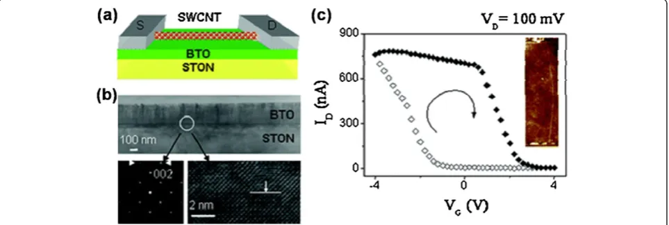
[image:7.595.57.540.89.228.2]Based on an excellent FE-CNT interface with few defects in the FE layer, an intrinsic ferroelectric memory FeFET was fabricated by integrating BTO with SWCNT [38]. The moderate preparation process has been carried out to reduce the interface reaction: BTO was pre-prepared on a smooth Nb-doped (001) SrTiO3(STON) substrate by pulsed laser deposition (PLD). Then, the Figure 9Schematic illustration of nanotetrapod transistor and images of CdS nanotetrapod and the fabricated device.(a) Schematic illustration of a nanotetrapod transistor with a 300-nm-thick ferroelectric dielectric under testing with scanning tunneling microscope (STM) tips. The source (S) and drain (D) electrodes are the patterned Pt layer. (b) Typical TEM image of the multiarmed CdS nanotetrapod used in this study. (c) The enlarged micrograph of a single CdS nanotetrapod. (d) SEM image of a single CdS nanotetrapod device. (e)In situSEM image of two STM tips (shown in white) probing on a testing device.
Table 1 The coupling between size effect and fatigue in different FE systems
Ferroelectric systems Size effect Fatigue behavior
Ferroelectrics Electrode Size effect Samples Fatigue Samples
BaTiO3, SrTiO3, BST, PZT Metal Yes BTO/metal, BST/Pt,
PZT/Pt, Ni/SrTiO3Pt
Yes BTO/metal, PZT/Pt
BaTiO3,SrTiO3,BST,PZT Electrolyte No BTO/LiCl No BTO/LiF
BaTiO3, SrTiO3, BST, PZT Oxide No PZT/RuO2,BST/IrO2,
BST/SRO,PZT/LSCO
No PZT/RuO2,PZT/SRO,
PZT/YBCO,PZT/LSCO
SBT Metal No SBT/Pt No SBT/Pt
Bi4Ti3O12 Metal Yes BIT/Ti–Ag Yes BIT/Au
Bi4Ti3O12 Oxide No BIT/CaRuO No BIT/Sb-doped SnO2, BIT/SRO
[image:7.595.56.541.589.732.2]temperate method of spin coating was utilized to deposit SWCNTs onto BTO. Figure 11a showed the schematic diagram of the memory device. The TEM image of the microstructure of the memory device was also displayed in Figure 11b, which revealed a coherent epitaxial growth of BTO on STON. The typical clockwise hysteresis loop
[image:8.595.57.540.89.357.2]was shown in Figure 11c. As we mentioned previously, theVthshift was in accordance with the variation of the sweeping region and the initial value. The Vthvalues of the device herein were 2.5 V and−1.5 V asVGswept up-ward and downup-ward, respectively, which supplied a wide memory window of 4 V. Thus, when a positive pulse was Figure 10I-VGtransfer characteristics.TypicalI-VGtransfer characteristic was measured at (a) 300, (b) 140, (c) 80, and (d) 8.5 K (withVDS= 2 V
for a to c;VDS= 50 mV for d). In (a), a counterclockwise hysteresis loop occurs at room temperature due to a charge-store effect. In (b), at 80 K, a
clockwise hysteresis loop is opened, indicating a nonvolatile memory operation. In (c), a competition between the ferroelectric effect and the charge-storage effect essentially closes the memory window at 140 K. In (d), at 8.5 K, a ferroelectric-modulated SET behavior is observed. The two red circles represent a bistable state. The sharp increase at a gate voltage of−6 V is due to the leakage current.
Figure 11Schematic sketch and TEM images of the CNT FeFET and theID-VGtransfer characteristics.(a) Schematic sketch of the fabricated CNT FeFET. (b) Structural characterization of BaTiO3thin films deposited on STON substrates by TEM, indicating the coherent epitaxial
growth of the BaTiO3thin film with respect to the STON substrate. (c) TypicalID-VGtransfer characteristics of the CNT FeFET made of SWCNT with
[image:8.595.58.540.523.685.2]applied on the active SWCNT channel (assuming a posi-tive voltage of drain-source), the polarization of BTO went from the FE layer towards the SWCNT. When the pulse was released, a high barrier was induced by the downward band bending of SWCNT. Hence, the device was effectively at off state, which could be defined as bin-ary 0. The binbin-ary 1 could be defined correspondingly as well. A series of homologous pulses tracking the hyster-esis loop could therefore realize a sequence of erases and writes. It should be noted that a compromised hysteresis loop has been observed when the gate voltage was below 1 V, as shown in Figure 12a, whereas the coercive voltage of the FE layer herein was about 2 V. To further investi-gate this interesting behavior, a theoretical simulation was performed. As shown in Figure 12b,c, the electric field at the interface between the SWCNT and FE layer was far more thanEC caused by the ultrathin SWCNT; thus, the device could still remain valid at the gate volt-age of less than 1 V. Therefore, CNT FeFET offers great
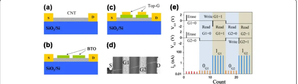
[image:9.595.58.540.89.225.2]potential for manufacturing low-power consumption NVMDs. For a coherent study of this work, a double-gate SWCNT FeFET (a two-bit memory device) was fab-ricated with the similar technology roadmaps. The sche-matic maps of the fabrication are shown in Figure 13a,b,c [38]. As a p-type intrinsic SWCNT FeFET memory de-vice, withVDS= 10 mV, the device was turned off when a positive gate pulse (2 V) was applied on both gates, which corresponded to the program process of erasing the information stored to binary state 00. The binary in-formation of 01 could be written into an individual FeFET by applying a low bias of −0.5 V on gate 2, which was lower than the threshold voltage yet not enough to induce an efficient polarization in the FE layer. As a result, gate 1 became off (binary 0 state) and gate 2 became on (binary 1 state). The whole program process is shown in Figure 13e, which exhi-bits a high mobility of approximately 103 cm2 V−1s−1 and an ultrahigh integration density of over 200 Gbit/ Figure 12Transfer characteristics of the device and calculated electric field mappings around the SWCNT channel.(a) Transfer
characteristics of the FeFET memory unit with a 300-nm-SWCNT as conducting channel. (b,c) Calculated electric field mappings around the SWCNT channel at 1 and 0.1 V gate voltages, respectively. The red dashed line in the scale bar indicates the measured coercive electric field of the ferroelectric film.
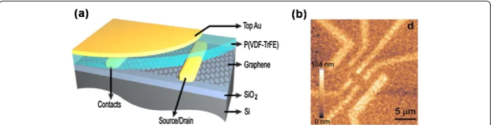
[image:9.595.57.541.538.674.2]Figure 14Schematic diagram and AFM image of a finished memory device.(a) Sample geometry of a finished memory device. (b) AFM image of the memory device. The contrast comes from the slightly different crystallization of PVDF-TrFE on SiO2, graphene, and Au electrodes, respectively.
Figure 15Electrical switch characteristics of the fabricated device.(a) Resistance hysteretic loop. The black curve represents the experimentally measured D of the PVDF-TrFE thin film with similar thickness. Inset (a): the electric displacement continuity equation at ferroelectric-graphene interface. Inset (b): a polarized PVDF-TrFE molecule. Cyan, gray, and white atoms represent fluorine, carbon, and hydrogen, respectively. (b) Electric hysteresis loop. R is used as a function of VTGfor the graphene-ferroelectric sample. From the linear part of this curve at high voltage, the charge carrier mobility is estimated
to be 700 cm2V−1s−1, takingκ
PVDF= 10. (c) Switching from 0 to 0 state in graphene-ferroelectric memory by a full loop sweep of VTG(±85 V). (d)
[image:10.595.62.538.242.665.2]in.2. This is highly desirable for the practical applications.
Graphene-based FeFET
Unlike the traditional semiconductor, graphene does not have bandgap. Therefore, the graphene-based FET usu-ally has poor on/off ratio at room temperature [81,82]. Although it has no advantages for digital switches, its high carrier mobility and excellent transconductance make it an ideal material for the radio frequency analog electronics in the logic integrated circuit [83-86]. The high carrier mobility also makes it a promising candidate for the next-generation ultrafast NVMDs [47,87]. More-over, the enhanced interfacial coupling makes the
performance of the graphene-based memory device much more elevated [43,46].
The graphene-based FeFET was fabricated using gra-phene as active channel (Figure 14a) [43]. A 700-nm-thick FE layer of poly(vinylidene fluoride-trifluoroethylene) (PVDF-TrFE) was then spin-coated on the graphene as the top gate. The atomic force microscopy (AFM) image (Figure 14b) showed that the FE layer has formed a con-tinuous thin film. With the switchable polarization of PVDF-TrFE, a resistance hysteretic loop with double peaks was obtained in Figure 15a, due to the induced dop-ing in graphene caused by the flippdop-ing electric dipoles. The binary states of 0 and 1 could then be defined as the minimum and the maximum values of R, respectively. With the closed hysteretic loop, the program processes could be realized by sweepingVGin the specific direction. Regardless of how the binary state transits, the program processes could be realized by following a full loop, as shown in Figure 15c,d,e,f. The graphene-based FeFET fea-tured a high carrier mobility of 200,000 cm2V−1s−1and a reading speed as fast as 10 fs. It should be further noted that the pronounced ΔR/R exceeded 200 %, which was essential for the retention time and fatigue resistance. These unique characteristics of graphene-based FeFET offer excellent potential in the applications of ultrafast FeFET-based NVMDs.
Challenges and improvements
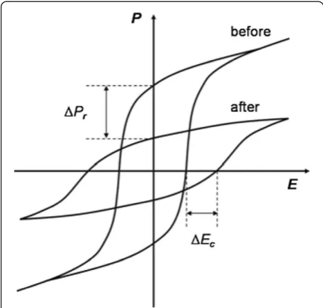
[image:11.595.56.290.89.312.2] [image:11.595.60.539.557.683.2]In the previous sections, we have introduced several excel-lent researches and their potential applications in the do-main of NVMDs. However, several inherent flaws have hindered its practical deployment, such as the endurance, fa-tigue, and retention time [88-91]. Theoretically, the charac-teristics of ferroelectric would not change. Nevertheless, the visualized experimental transformation of the hysteretic loop of the FE layer revealed that after a number of repetitive bi-polar switching cycles,Pr decreased andECincreased [92] (Figure 16). As a result, the smallerPrmay not be able to
Figure 16Hysteresis loops before and after bipolar fatigue.The loops show decrease in polarization and sometimes an increase in coercive field (particularly for ceramics).
Figure 17The schematic structure and memory performance of the device.(a) Pt-SrBi2Ta2O9-Hf-Al-O-Si MFIS FET. (b) Data retention
characteristic of the Pt-SrBi2Ta2O9-Hf-Al-O-Si FET. After application of the poling voltages ±6 V, the drain currents of both on and off states were
measured as a function of time.Vkeep=1.7 V andVD=0.1 V. (c) Endurance cycle performance of the Pt-SrBi2Ta2O9-Hf-Al-O-Si FET. The applied switching
induce enough carriers in the active channel and would lead to difficulty in distinguishing the binary signal 0 and 1, which consequently stops the memory device. Moreover, a larger ECmeans that a higher bias is required to switch the device. More researches therefore have been done to overcome these problems, including the introduction of new technolo-gies and new materials to get enhanced performance.
Oxide conductor as electrodes
[image:12.595.59.540.89.398.2]According to the model proposed by Dawber [93] and Scott [94], oxygen vacancies in ferroelectric films are believed to be able to impact the fatigue. Due to the local phase decomposition of ferroelectric and the oxy-gen vacancy migration towards the FE-electrode inter-face, accumulating and forming a pin structure, the Figure 18Schematic illustration of DPN method, the AFM image, and memory performance of the fabricated device.(a) Preparation of an Au-metal gate using AuCl4solution with a writing speed of approximately 300 nm/s by the DPN method. (b) A CNT-based nonvolatile memory device made
of a CNT channel, a nanostructured PVDF-TrFE-gate insulator, and an Au-metal gate. (c) AFM image of the CNT-based nonvolatile memory device, entirely composed of nanostructured elements. (d) Two retainedIDSstates plotted as a function of the relaxation time. (e) Fatigue-test result of the
PVDF-TrFE-based FET memory device.
[image:12.595.55.540.567.713.2]remnant polarization is dramatically decreased [95]. In the typical example of PZT, the oxide conductive materi-als were utilized as the electrodes [96], which effectively blocked the diffusion effect in each interface. The crys-talline structures therefore were not corroded, showing no fatigue behavior. The size effect was associated to the fatigue behavior as well. Table 1 shows a few ferroelec-tric systems and the characteristics of size effect in rela-tion to fatigue behavior [97].
Insert buffer
After a number of switch cycles, the carriers in the semi-conductor may inject into the FE layer, which deteriorated the dielectric constant of the FE layer. Moreover, the re-duction of remnant polarization was observed after modu-lating the VG, as proved by extensive experiments [98-100]. Therefore, a high κ buffer was introduced between the FE layer and semiconductor. On one hand, the buffer acted as the diffusion barrier to prevent the ferroelectric from being deteriorated [101]. On the other hand, though the superposed layers were equivalent to two serial capaci-tors, it made the voltage at the FE layer only slightly smal-ler than the initial gate voltage [53]. The representative work has been carried out in the early days, which inserted a 13-nm-thick buffer insulation layer of (HfO2)0.75(Al2O3)
0.25between p-type Si and a 400-nm-thick FE layer of SBT [14]. Figure 17a shows the schematic structure of the de-vice. As shown in Figure 17b,c, it retained an on/off ratio of more than 106 even after 12 days and endured 1012 cycles with no changes. Due to the superior retention and endurance, considerable researches have been done to ex-ploit this for practical applications.
Reduction of interfacial states
The scientific experiments have demonstrated that the interface quality of the device is essential for the fatigue be-havior [102,103]. The reduced interaction is beneficial for the fatigue resistance, which was demonstrated by the researches executing a post annealing to obtain enhanced performance [19]. Many new technologies and new materi-als were materi-also introduced to enhance the fatigue resistance, such as the position controllable dip-pen nanolithography (DPN) technology [104]. In this work, PVDF-TrFE was used as the ferroelectric gate. Unlike the inorganic ferro-electric, organic ferroelectric (PVDF-TrFE) has temperate chemical affinity and lower interfacial tension towards the CNT channel, which led to fewer defects in the interface. Figure 18a,b shows the visualized schematic technology maps of the fabricating process, and Figure 18c was the AFM image of the CNT-based nonvolatile memory device. The introduction of nanodot ferroelectric gate (approxi-mately 9.2 nm) realized a high integration density of the memory device, with the bistable state remarkably well retained at up to 106s. Moreover, as shown in Figure 18d,e,
even after approximately 1010 switching cycles, the two states were still distinguishable, demonstrating great performance.
Conclusions
In this paper, we explain the operating principles of FeFET and review several excellent researches on the integration of semiconductor materials with ferroelectric to achieve agreeable memory performance. The advantages of the nonvolatility and NDRO process make FeFET ideal for memory applications. With the development of material fabrication technologies, the non-planar ferroelectric nanostructures such as FE NWs [105-107], nanotube [108-110], and NPs [108] have been prepared successfully. Although the capacity of the first FeRAM had only a 256-bit density [111], with the incorporation of the modern semiconductor technology, ferroelectric nanostructures with much higher integration density have been integrated in a large scale [112,113]. The integration density can be further enhanced with new technologies and/or new de-vice structures. Based on the current achievements on the controllable and selective growth of CNT arrays, as shown in Figure 19a, we suggest a new FeFET architecture by in-tegrating CNT arrays with ferroelectric to further enhance the integration density of the memory devices. While current FeFET advancements have supplied potential routes to overcome the scale limitations and economic challenges, the fatigue and retention time remain as the main challenges hindering the practical applications. It still will be a long way to go to realize the mass commercial production.
Competing interests
The authors declare that they have no competing interests.
Authors’contributions
XL wrote and revised the manuscript. YL and WC suggested many helpful and interesting issues for improving the review paper. JL revised the paper thoroughly. LL drafted and revised the manuscript. All authors read and approved the final manuscript.
Acknowledgments
This work was supported by the MOE NCET-10-0643 and NSFC grant (nos. 11104207 and 10975109) as well as‘the grant of state key laboratory of advanced technology for materials synthesis and processing (Wuhan University of Technology)’.
Author details
1Key Laboratory of Artificial Micro- and Nano-structures of Ministry of
Education, and School of Physics and Technology, Wuhan University, Wuhan 430072, People's Republic of China.2State Key Laboratory of Advanced
Technology for Materials Synthesis and Processing, and School of Materials Science and Engineering, Wuhan University of Technology, Wuhan 430070, People's Republic of China.
Received: 17 February 2012 Accepted: 23 April 2012 Published: 1 June 2012
References
2. Liao L, Fan H, Yan B, Zhang Z, Chen L, Li B, Xing G, Shen Z, Wu T, Sun X: Ferroelectric transistors with nanowire channel: toward nonvolatile memory applications.ACS Nano2009,3:700–706.
3. Tue PT, Miyasako T, Trinh BNQ, Li J, Tokumitsu E, Shimoda T:Optimization of Pt and PZT films for ferroelectric-gate thin film transistors.Ferroelectrics
2010,405:281–291.
4. Heremans P, Gelinck GH, Muller R, Baeg KJ, Kim DY, Noh YY:Polymer and organic nonvolatile memory devices.Chem Mater2011,23:341–358. 5. Xie D, Ren TL, Liu LT:M/Bi3.4La0.6Ti3O12/I/Si capacitors for the application
in FEDRAM. InProceedings of 2007 International Workshop on Electron Devices and Semiconductor Technology: June 3–4 2007; Beijing. Washington D.C: IEEE; 2007:74–77.
6. Arimoto Y, Ishiwara H:Current status of ferroelectric random-access memory.MRS Bull2004,29:823–828.
7. Wang H, Wu Y, Cong C, Shang J, Yu T:Hysteresis of electronic transport in graphene transistors.ACS nano2010,4:7221–7228.
8. Ling QD, Lim SL, Song Y, Zhu CX, Chan DSH, Kang ET, Neoh KG: Nonvolatile polymer memory device based on bistable electrical switching in a thin film of poly (n-vinylcarbazole) with covalently bonded C60.Langmuir2007,23:312–319.
9. Mukherjee B, Mukherjee M:Nonvolatile memory device based on Ag nanoparticle: characteristics improvement.Appl Phys Lett2009,94:173510. 10. Gerra G, Tagantsev AK, Setter N:Ferroelectricity in asymmetric
metal-ferroelectric-metal heterostructures: a combined first-principles phenomenological approach.Phys Rev Lett2007,98:207601.
11. Kornev IA, Fu H, Bellaiche L:Properties of ferroelectric ultrathin films from first principles.J Mater Sci2006,41:137–145.
12. Gruverman A, Kholkin A:Nanoscale ferroelectrics: processing, characterization and future trends.Rep Prog Phys2006,69:2443. 13. Shaw T, Trolier-McKinstry S, McIntyre P:The properties of ferroelectric films
at small dimensions.Annu Rev Mater Sci2000,30:263–298.
14. Sakai S, Ilangovan R:Metal-ferroelectric-insulator-semiconductor memory FET with long retention and high endurance.IEEE Electron Device Lett.
2004,25:369–371.
15. Tue PT, Bui NQT, Miyasako T, Tokumitsu E, Shimoda T:Fabrication and characterization of a ferroelectric-gate FET With a ITO/PZT/SRO/Pt stacked structure. InInternational Conference on Microelectronics: December 19–22 2010; Cairo. New York: IEEE; 2010:32–35.
16. Hutchby JA, Bourianoff GI, Zhirnov VV, Brewer JE:Extending the road beyond CMOS.IEEE Circuits Devices Mag.2002,18:28–41.
17. Sohn JI, Choi SS, Morris SM, Bendall JS, Coles HJ, Hong WK, Jo G, Lee T, Welland ME:Novel nonvolatile memory with multibit storage based on a ZnO nanowire transistor.Nano Lett2010,10:4316–4320.
18. Jimenez D, Miranda E, Godoy A:Analytic model for the surface potential and drain current in negative capacitance field-effect transistors.IEEE Trans Electron Devices2010,57:2405–2409.
19. Yoon SM, Yang SH, Jung SW, Byun CW, Park SHK, Hwang CS, Lee GG, Tokumitsu E, Ishiwara H:Impact of interface controlling layer of Al2O3for
improving the retention behaviors of InGaZn oxide-based ferroelectric memory transistor.Appl Phys Lett2010,96:232903.
20. Horenstein MN, Sumner R, Miller P, Bifano T, Stewart J, Cornelissen S: Ultra-low-power multiplexed electronic driver for high resolution deformable mirror systems. InProceedings of SPIE 7930,7930M1: January 24 2011; San Francisco. Bellingham: SPIE; 2011.
21. Brewer JE, Zhirnov VV, Hutchby JA:Memory technology for post CMOS era.IEEE Circuits Devices Mag.2005,21:13–20.
22. Kubel F, Schmid H:Structure of a ferroelectric and ferroelastic monodomain crystal of the perovskite BiFeO3.Acta Crystallogr., Sect. B:
Struct. Sci1990,46:698–702.
23. Kang SJ, Bae I, Shin YJ, Park YJ, Huh J, Park SM, Kim HC, Park C:Nonvolatile Polymer memory with nanoconfinement of ferroelectric crystals.Nano Lett2011,11:138–144.
24. Pradhan MR, Rajan E:A system engineering approach to molecular electronics.International Journal of Computer Applications IJCA2010, 3:14–23.
25. Lei B, Li C, Zhang D, Zhou Q, Shung K, Zhou C:Nanowire transistors with ferroelectric gate dielectrics: enhanced performance and memory effects.Appl Phys Lett2004,84:4553–4555.
26. Shen Z, Chen Z, Li H, Qu X, Chen Y, Liu R:Nanoembossing and piezoelectricity of ferroelectric Pb (Zr0. 3,Ti0. 7)O3nanowire arrays.Appl
Surf Sci2011,257:8820–8823.
27. Chiang YD, Chang WY, Ho CY, Chen CY, Ho CH, Lin SJ, Wu TB, He JH: Single-ZnO-nanowire memory.IEEE Trans Electron Devices. 2011, 58:1735–1740.
28. Yang Y, Zhang X, Gao M, Zeng F, Zhou W, Xie S, Pan F:Nonvolatile resistive switching in single crystalline ZnO nanowires.Nanoscale2011, 3:1917–1921.
29. Chen SW, Lee CC, Chen MT, Wu JM:Synthesis of BiFeO3/ZnO core–shell
hetero-structures using ZnO nanorod positive templates.Nanotechnology
2011,22:115605.
30. Kim HJ, Jung SM, Kim YH, Kim BJ, Ha S, Kim YS, Yoon TS, Lee HH: Characterization of gold nanoparticle pentacene memory device with polymer dielectric layer.Thin Solid Films2011,519:6140–6143. 31. Wang S, Yang H, Xian T, Liu X:Size-controlled synthesis and
photocatalytic properties of YMnO3nanoparticles.Catal Commun2010,
12:625–628.
32. Mokhnatyuk A:Three-dimensional optical memory in ferroelectric media. J. Russ. Laser Res.1999,20:279–295.
33. Lowrey TA, Duesman KG, Cloud EH:Method of making a 3-dimensional programmable antifuse for integrated circuits.Patent US5324681, June 28 1994.
34. Ou E, Wong SS:Array architecture for a nonvolatile 3-dimensional cross-point resistance-change memory.IEEE J Solid State Circuits2011, 46:2158–2170.
35. Fu W, Qin S, Liu L, Kim TH, Hellstrom S, Wang W, Liang W, Bai X, Li AP, Wang E:Ferroelectric gated electrical transport in CdS nanotetrapods. Nano Lett.2011,11:1913–1918.
36. Fuhrer M, Kim B, Dürkop T, Brintlinger T:High-mobility nanotube transistor memory.Nano Lett.2002,2:755–759.
37. Ishiwara H:Current status of ferroelectric-gate Si transistors and challenge to ferroelectric-gate CNT transistors.Curr Appl Phys2009,9:S2–S6. 38. Fu W, Xu Z, Bai X, Gu C, Wang E:Intrinsic memory function of carbon
nanotube-based ferroelectric field-effect transistor.Nano Lett2009, 9:921–925.
39. Fu W, Xu Z, Liu L, Bai X, Wang E:Two-bit ferroelectric field-effect transistor memories assembled on individual nanotubes.Nanotechnology
2009,20:475305.
40. Rinkio M, Johansson A, Paraoanu G, Torma P:High-speed memory from carbon nanotube field-effect transistors with high-κgate dielectric.Nano Lett2009,9:643–647.
41. Meunier V, Kalinin SV, Sumpter BG:Nonvolatile memory elements based on the intercalation of organic molecules inside carbon nanotubes.Phys Rev Lett2007,98:56401.
42. Naber RCG, Tanase C, Blom PWM, Gelinck GH, Marsman AW, Touwslager FJ, Setayesh S, De Leeuw DM:High-performance solution-processed polymer ferroelectric field-effect transistors.Nat Mater2005,4:243–248.
43. Zheng Y, Ni GX, Toh CT, Zeng MG, Chen ST, Yao K, Özyilmaz B: Gate-controlled nonvolatile graphene-ferroelectric memory.Appl Phys Lett
2009,94:163505.
44. Naber RCG, Asadi K, Blom PWM, De Leeuw DM, De Boer B:Organic nonvolatile memory devices based on ferroelectricity.Adv Mater2010, 22:933–945.
45. Kim TW, Gao Y, Acton O, Yip HL, Ma H, Chen H, Alex KYJ:Graphene oxide nanosheets based organic field effect transistor for nonvolatile memory applications.Appl Phys Lett2010,97:023310.
46. Hong X, Hoffman J, Posadas A, Zou K, Ahn C, Zhu J:Unusual resistance hysteresis in n-layer graphene field effect transistors fabricated on ferroelectric Pb(ZrTi)O.Appl Phys Lett2010,97:033114.
47. Doh YJ, Yi GC:Nonvolatile memory devices based on few-layer graphene films.Nanotechnology2010,21:105204.
48. Zheng Y, Ni GX, Bae S, Cong CX, Kahya O, Toh CT, Kim HR, Im D, Yu T, Ahn JH:Wafer-scale graphene/ferroelectric hybrid devices for low-voltage electronics.Europhys Lett2011,93:17002.
49. Zheng Y, Ni GX, Toh CT, Tan CY, Yao K, Özyilmaz B:Graphene field-effect transistors with ferroelectric gating.Phys Rev Lett2010,105:166602. 50. Hill NA:Why are there so few magnetic ferroelectrics?J Phys Chem B
2000,104:6694–6709.
51. Dawber M, Rabe K, Scott J:Physics of thin-film ferroelectric oxides.Rev Mod Phys2005,77:1083.
53. Yeh CS, Wu JM:Characterization of Pt/multiferroic BiFeO/(Ba, Sr)TiO/Si stacks for nonvolatile memory applications.Appl Phys Lett2008, 93:154101.
54. Liao M, Imura M, Fang X, Nakajima K, Chen G, Koide Y:Integration of (PbZrTiO) on single crystal diamond as metal-ferroelectric-insulator -semiconductor capacitor.Appl Phys Lett2009,94:242901.
55. Liu X, Ji ZY, Liu M, Shang LW, Li DM, Dai YH:Advancements in organic nonvolatile memory devices.Chin Sci Bull2011,56:3178–3190. 56. Lin CM, Shih W, Chang IY, Juan PC, Lee JY:Metal-ferroelectric
(BiFeO)-insulator (YO)-semiconductor capacitors and field effect transistors for nonvolatile memory applications.Appl Phys Lett2009,94:142905. 57. Shiga H, Takashima D, Shiratake S, Hoya K, Miyakawa T, Ogiwara R, Fukuda
R, Takizawa R, Hatsuda K, Matsuoka F:A 1.6 GB/s DDR2 128 Mb chain FeRAM with scalable octal bitline and sensing schemes.IEEE J Solid State Circuits2010,45:142–152.
58. Velev JP, Duan CG, Belashchenko KD, Jaswal S, Tsymbal EY:Effect of ferroelectricity on electron transport in Pt/BaTiO3/Pt tunnel junctions.
Phys Rev Lett2007,98:137201.
59. Im JH, Jeon HS, Kim JN, Kim DW, Park BE, Kim CJ:Ferroelectric properties of SrBi2Ta2O9thin films on Si (100) with a LaZrOxbuffer layer.
J Electroceram.2009,22:276–280.
60. Alexe M, Harnagea C, Visinoiu A, Pignolet A, Hesse D, Gsele U:Patterning and switching of nano-size ferroelectric memory cells.Scr Mater2001, 44:1175–1179.
61. Rinkio M, Johansson A, Paraoanu G, Torma P:High-speed memory from carbon nanotube field-effect transistors with high-кgate dielectric.Nano Lett.2009,9:643–647.
62. Naber R, De Boer B, Blom P, De Leeuw D:Low-voltage polymer field-effect transistors for nonvolatile memories.Appl Phys Lett2005,87:203509. 63. Kim K, Lee S:Integration of lead zirconium titanate thin films for high
density ferroelectric random access memory.J Appl Phys2006, 100:051604.
64. Goux L, Xu Z, Kaczer B, Groeseneken G, Wouters DJ:Deposition of 60 nm thin Sr0.8Bi2.2Ta2O9layers for application in scaled 1T1C and 1T FeRAM
devices.Microelectron Eng2005,80:162–165.
65. Lee KH, Lee G, Lee K, Oh MS, Im S, Yoon SM:High-mobility nonvolatile memory thin-film transistors with a ferroelectric polymer interfacing ZnO and pentacene channels.Adv Mater2009,21:4287–4291.
66. Lau S, Zheng R, Chan H, Choy C:Preparation and characterization of poly (vinylidene fluoride-trifluoroethylene) copolymer nanowires and nanotubes.Mater Lett2006,60:2357–2361.
67. Lai EK, Lue HT, Hsieh KY:Stacked thin film transistor, non-volatile memory devices and methods for fabricating the same.Patent, US7999295. August 16 2011.
68. Lee W, Aw K, Wong H, Chan K, Leung M, Salim NT:An organic thin film transistor based non-volatile memory with zinc oxide nanoparticles.Thin Solid Films2011,519:5208–5211.
69. Suresh A, Novak S, Wellenius P, Misra V, Muth JF:Transparent indium gallium zinc oxide transistor based floating gate memory with platinum nanoparticles in the gate dielectric.Appl Phys Lett2009, 94:123501.
70. Yoon SM, Yang SH, Ko Park SH, Jung SW, Cho DH, Byun CW, Kang SY, Hwang CS, Yu BG:Effect of ZnO channel thickness on the device behaviour of nonvolatile memory thin film transistors with double-layered gate insulators of Al2O3and ferroelectric polymer.J. Phys. D: Appl.
Phys.2009,42:245101.
71. Kim HW, Kim NH, Shim JH, Cho NH, Lee C:Catalyst-free MOCVD growth of ZnO nanorods and their structural characterization.J Mater Sci Mater Electron2005,16:13–15.
72. Park C, Im S, Yun J, Lee GH, Lee BH, Sung MM:Transparent photostable ZnO nonvolatile memory transistor with ferroelectric polymer and sputter-deposited oxide gate.Appl Phys Lett2009,95:223506. 73. Liao L, Li J, Liu D, Liu C, Wang D, Song W, Fu Q:Self-assembly of aligned
ZnO nanoscrews: Growth, configuration, and field emission.Appl Phys Lett2005,86:083106.
74. Prakash J, Choudhary A, Kumar A, Mehta D, Biradar A:Nonvolatile memory effect based on gold nanoparticles doped ferroelectric liquid crystal. Appl Phys Lett2008,93:112904.
75. Li Q, Zhu X, Xiong HD, Koo SM, Ioannou D, Kopanski JJ, Suehle J, Richter C: Silicon nanowire on oxide/nitride/oxide for memory application. Nanotechnology2007,18:235204.
76. Javey A, Guo J, Wang Q, Lundstrom M, Dai H:Ballistic carbon nanotube field-effect transistors.Nature2003,424:654–657.
77. Nishio T, Miyato Y, Kobayashi K, Ishida K, Matsushige K, Yamada H:The effect of local polarized domains of ferroelectric P(VDF/TrFE) copolymer thin film on a carbon nanotube field-effect transistor. Nanotechnology2008,19:035202.
78. Artukovic E, Kaempgen M, Hecht D, Roth S, Grüner G:Transparent and flexible carbon nanotube transistors.Nano Lett.2005,5:757–760. 79. Bradley K, Gabriel JCP, Grüner G:Flexible nanotube electronics.Nano Lett.
2003,3:1353–1355.
80. Lee JD, Hur SH, Choi JD:Effects of floating-gate interference on NAND flash memory cell operation.IEEE Electron Device Lett.2002,23:264–266. 81. Kim S, Nah J, Jo I, Shahrjerdi D, Colombo L, Yao Z, Tutuc E, Banerjee SK:
Realization of a high mobility dual-gated graphene field-effect transistor with Al2O3dielectric.Appl Phys Lett2009,94:062107–062103.
82. Wang X, Ouyang Y, Li X, Wang H, Guo J, Dai H:Room-temperature all-semiconducting sub-10-nm graphene nanoribbon field-effect transistors. Phys Rev Lett2008,100:206803.
83. Liao L, Bai J, Lin YC, Qu Y, Huang Y, Duan X:High-performance top-gated graphene-nanoribbon transistors using zirconium oxide nanowires as high dielectric constant gate dielectrics.Adv Mater2010, 22:1941–1945.
84. Liao L, Bai J, Cheng R, Lin YC, Jiang S, Qu Y, Huang Y, Duan X:Sub-100 nm channel length graphene transistors.Nano Lett.2010,10:3952–3956. 85. Liao L, Bai J, Qu Y, Lin Y, Li Y, Huang Y, Duan X:High-кoxide nanoribbons
as gate dielectrics for high mobility top-gated graphene transistors. PNAS2010,107:6711.
86. Liao L, Duan X:Graphene-dielectric integration for graphene transistors. Mater Sci Eng R2010,:(70) 354–370.
87. Meric I, Han MY, Young AF, Ozyilmaz B, Kim P, Shepard KL:Current saturation in zero-bandgap, top-gated graphene field-effect transistors. Nat Nanotechnol2008,3:654–659.
88. Kato Y, Kaneko Y, Tanaka H, Kaibara K, Koyama S, Isogai K, Yamada T, Shimada Y:Overview and future challenge of ferroelectric random access memory technologies.Jpn J Appl Phys2007,46:2157–2163.
89. Gysel R, Stolichnov I, Tagantsev AK, Riester SWE, Setter N, Salvatore GA, Bouvet D, Ionescu AM:Retention in nonvolatile silicon transistors with an organic ferroelectric gate.Appl Phys Lett2009,94:263507.
90. Ren TL, Zhang MM, Jia Z, Wang LK, Wei CG, Xue KH, Zhang YJ, Hu H, Xie D, Liu LT:Model and key fabrication technologies for FeRAM. In2009 International Conference on Semiconductor Technology for Ultra Large Scale Integrated Circuits and Thin Film Transistors (ULSIC vs. TFT): July 5–10 2009; Xi'an. Edited by Kuo Y. Pennington: ECS; 2009:217.
91. Jeong Hwan K, Park BE, Ishiwara H:Fabrication and electrical
characteristics of metal-ferroelectric-semiconductor field effect transistor based on poly (vinylidene fluoride).Jpn J Appl Phys2008,47:8472–8475. 92. Lou X:Polarization fatigue in ferroelectric thin films and related
materials.J Appl Phys2009,105:024101–024124.
93. Dawber M, Scott J:A model for fatigue in ferroelectric perovskite thin films.Appl Phys Lett2000,76:1060–1062.
94. Scott J, Dawber M:Oxygen-vacancy ordering as a fatigue mechanism in perovskite ferroelectrics.Appl Phys Lett2000,76:3801.
95. Lou X, Zhang M, Redfern S, Scott J:Local phase decomposition as a cause of polarization fatigue in ferroelectric thin films.Phys Rev Lett2006, 97:177601.
96. Fe L, Wouters D:Effect of RuO2growth temperature on ferroelectric
properties of RuO2/Pb (Zr, Ti) O3/RuO2/Pt capacitors.Appl Phys Lett2000,
76:1318–1320.
97. Jin H, Zhu J:Size effect and fatigue mechanism in ferroelectric thin films. J Appl Phys2002,92:4594.
98. Juan TP, Chang C, Lee JY:A new metal-ferroelectric (PbZr0. 53Ti0. 47O3)-insulator (Dy2O3)-semiconductor (MFIS) FET for nonvolatile
memory applications.IEEE Electron Device Lett.2006,27:217–220. 99. Luo YF, Xie D, Zang YY, Song R, Ren TL, Liu LT:Buffer layer
dependence of B3.15Nd0.85Ti3O12(BNdT) based MFIS capacitor for
FeFET application. In2008 9th International Conference on Solid-State and Integrated-Circuit Technology: October 20–23 2008; Beijing. Edited by Huang R. Washington D.C: IEEE; 2008:2592.
100. Yang C, Hu G, Wen Z, Yang H:Effects of Bi2Ti2O7buffer layer on memory
101. Murari N, Thomas R, Pavunny S, Calzada J, Katiyar R:DyScO3buffer layer
for a performing metal-ferroelectric-insulator-semiconductor structure with multiferroic BiFeO3thin film.Appl Phys Lett2009,94:142907–142903. 102. Park C, Lee G, Lee KH, Im S, Lee BH, Sung MM:Enhancing the retention
properties of ZnO memory transistor by modifying the channel/ ferroelectric polymer interface.Appl Phys Lett2009,95:153502. 103. Park CH, Lee KH, Lee BH, Sung MM, Im S:Channel/ferroelectric interface
modification in ZnO non-volatile memory TFT with P(VDF-TrFE) polymer. J Mater Chem2009,20:2638–2643.
104. Son JY, Ryu S, Park YC, Lim YT, Shin YS, Shin YH, Jang HM:A nonvolatile memory device made of a ferroelectric polymer gate nanodot and a single-walled carbon nanotube.ACS Nano2010,4:7315–7320. 105. Wang Z, Hu J, Yu MF:One-dimensional ferroelectric monodomain
formation in single crystalline BaTiO nanowire.Appl Phys Lett2006, 89:263119.
106. Zhang X, Zhao X, Lai C, Wang J, Tang X, Dai JY:Synthesis and piezoresponse of highly ordered Pb(Zr0. 53Ti0. 47)O3 nanowire arrays. Appl Phys Lett2004,85:4190–4192.
107. Wang J, Sandu C, Colla E, Wang Y, Ma W, Gysel R, Trodahl H, Setter N, Kuball M:Ferroelectric domains and piezoelectricity in monocrystalline Pb(Zr, Ti)O nanowires.Appl Phys Lett2007,90:133107.
108. Alexe M, Hesse D, Schmidt V, Alexe M, Hesse D, Schmidt V, Senz S, Fan H, Zacharias M, Gsele U:Ferroelectric nanotubes fabricated using nanowires as positive templates.Appl Phys Lett2006,89.
109. Feng M, Wang W, Zhou Y, Jia D:Synthesis and characterization of ferroelectric SrBi2Ta2O9nanotubes arrays.J Sol–gel Sci Technol2009,
52:120–123.
110. Seo B, Shaislamov U, Kim SW, Kim HK, Yang B, Hong S:Bi3. 25La0. 75Ti3O12
(BLT) nanotube capacitors for semiconductor memories.Physica E2007, 37:274–278.
111. Takashima D:Overview and scaling prospect of ferroelectric memories. CMOS Processors and Memories2010,:36–380.
112. Choi WB, Bae E, Kang D, Chae S, Cheong B, Ko J, Lee E, Park W:Aligned carbon nanotubes for nanoelectronics.Nanotechnology2004,15:S512. 113. Sun Y, Fuge GM, Ashfold MNR:Growth mechanisms for ZnO nanorods
formed by pulsed laser deposition.Superlattices Microstruct2006, 39:33–40.
doi:10.1186/1556-276X-7-285
Cite this article as:Liuet al.:Ferroelectric memory based on nanostructures.Nanoscale Research Letters20127:285.
Submit your manuscript to a
journal and benefi t from:
7 Convenient online submission
7 Rigorous peer review
7 Immediate publication on acceptance
7 Open access: articles freely available online
7 High visibility within the fi eld
7 Retaining the copyright to your article