N A N O E X P R E S S
Open Access
Effects of Rapid Thermal Annealing and
Different Oxidants on the Properties of
La
x
Al
y
O Nanolaminate Films Deposited by
Atomic Layer Deposition
Chenxi Fei , Hongxia Liu
*, Xing Wang, Lu Zhao, Dongdong Zhao and Xingyao Feng
Abstract
A comparative study of different sequences of two metal precursors [trimethylaluminum (TMA) and
Tris(isopropylcyclopentadienyl) lanthanum (La(iPrCp)3)] for atomic layer deposition (ALD) lanthanum aluminum oxide (LaxAlyO) films is carried out. The percentage compositions of C and N impurity of LaxAlyO films were investigated using in situ X-ray photoelectron spectroscopy (XPS). The effects of different oxidants on the physical and chemical properties and electrical characteristics of LaxAlyO films are studied before and after annealing. Preliminary testing results indicate that the impurity level of LaxAlyO films grown with different oxidants can be well controlled before and after annealing. Analysis indicates the rapid thermal annealing (RTA) and kinds of oxidants have significant effects on the equivalent oxide thickness (EOT), dielectric constant, electrical properties, and stability of LaxAlyO films. Additionally, the change of chemical bond types of rapid thermal annealing effects on the properties of LaxAlyO films are grown with different oxidants also investigated by XPS.
Keywords:ALD, X-ray photoelectron spectroscopy, Rapid thermal annealing, EOT
Background
The miniaturization of complementary metal-oxide-semiconductor (CMOS) devices would eventually re-quire the thinning of a gate dielectric, whose capacitance should be equivalent to that of SiO2with a thickness less
than 1 nm. Ultrathin SiO2as a gate dielectric has been
rapidly confronted with its fundamental limit due to its unacceptably high leakage current. The replacement of SiO2 with high dielectric constant (k) materials has
re-cently attracted considerable attention because their large physical thickness can suppress a gate tunneling leakage current at a scaled equivalent oxide thickness (EOT) [1–4]. Several candidate materials for the gate di-electric films such as HfO2 [5], ZrO2 [6], La2O3 [7],
Y2O3 [8], Ta2O5 [9], and Al2O3 [10] have been studied
extensively during the past decade. As a promising high-k material, La2O3has advantages of high dielectric constant
(~30) and good thermal stability, but the hygroscopicity
would lead to high leakage [11]. Al2O3has many favorable
properties like kinetic stability and thermodynamic stabil-ity on Si up to high temperatures, good interface with Si, and low bulk defect density. However, the dielectric con-stant of Al2O3 (~9) is low [12]. Lanthanum aluminate
(LaAlO3 or LAO), which is a compound of La2O3 and
Al2O3, is a promising material as it possesses a large
band-gap (5–6 eV), a high dielectric constant (22–25), and a relatively large band offset with Si (2 eV)[13].
Various deposition techniques such as molecular beam epitaxy (MBE) [14], pulsed laser deposition (PLD) [15], metal-organic chemical vapor deposition (MOCVD) [16], and atomic layer deposition (ALD) have been explored to grow the high-kdielectric layers on Si sub-strate [17]. ALD is a method of cyclic deposition and oxidation which consists of alternate pulsing of the pre-cursor gases and vapors on the substrate surface result-ing in subsequent chemisorptions or surface reaction of the precursors to produce the desired oxide. Under suit-able conditions, ALD is a saturation reaction with con-stant thickness increase in each deposition cycle. Hence,
* Correspondence:hxliu@mail.xidian.edu.cn
Key Laboratory for Wide-Band Gap Semiconductor Materials and Devices of Education, School of Microelectronics, Xidian University, Xi’an 710071, China
regardless of the precursor dose supplied, the resulting thickness will always be the same, if the appropriate saturation dose is supplied. This is termed as the self-limiting growth mechanism of ALD which facilitates the growth of conformal thin films with accurate thickness control. ALD is also suitable for depositions on trench-type structures. Also, for thin films, the ALD produces better uniformity and lesser defects as compared to other deposition techniques [18, 19]. These qualities make the ALD method attractive for manufacturing of future generation integrated circuits especially gate dielectric applications.
Various oxygen sources have been used in the past for ALD such as O3, O2, and, the most common, H2O. The
oxidation power of the oxygen source towards the bare Si surface is very important in ALD to achieve low EOT values, since growth of low k layer such as SiOx can
reduce the overall capacitance. In order to obtain low charge leakage, residual impurities in the high-k film should be reduced as much as possible. The oxidants have great influences on the defects and residual impur-ities in the high-kfilm if the process conditions are opti-mized in ALD process. On the other hand, the effects of RTA on the properties of LaxAlyO films have been
reported [20, 21]. People found that the growth of the interface layer was suppressed and the properties of film were enhanced by RTA. However, the oxidant effects on the characteristics of LaxAlyO before and after annealing
have rarely been discussed. In this study, two kinds of oxidants (H2O and O3) are used to deposit LaxAlyO
films by ALD. The effects of the different combinations of the different oxidants with metal precursors on the physical, electrical, and chemical properties of annealed LaxAlyO films are investigated.
Methods
A P-type Si B-doped (100) wafer with a resistivity of 8–12 Ω cm was cleaned with a (HCl:H2O2:H2O = 1:1:5)
solution for 10 min at 85 °C to remove organic contamin-ation and then chemically etched with a diluted hydro-fluoric acid solution (HF:H2O = 1:100) to remove native
oxides, both followed by a 30-s rinse in deionized water. LaxAlyO films were deposited on Si wafers by a
layer-by-layer deposition process using different metal processors (trimethylaluminum (TMA) and tris(isopropylcyclopenta-dienyl) lanthanum [La(iPrCp)3]) and oxidants (H2O and
O3) at 300 °C by ALD reactor (Picosun R-200, Espoo,
Finland). Ultra-high purity nitrogen (N2, 99.999%) was
employed as carrier and purge gas. The container of the TMA is at room temperature, corresponding to a vapor pressure of 10 to 15 hPa, and La(iPrCp)3 was kept at
180 °C, respectively. When H2O is used as an oxidant,
ALD sequence was composed of 0.5 s La(iPrCp)3pulse/6 s
purge with N2/0.5 s H2O pulse/8 s purge with N2 and
0.1 s TMA pulse/3 s purge with N2/0.1 s H2O pulse/4 s
purge with N2. When O3is used as an oxidant, ALD
se-quence was composed of 0.5 s La(iPrCp)3pulse/8 s purge
with N2/0.5 s O3pulse/10s purge with N2and 0.1 s TMA
pulse/3 s purge with N2/0.5 s O3pulse/4 s purge with N2.
Post-deposition annealing (PDA) was performed for 60 s in N2 ambient at 600 °C using rapid thermal annealing
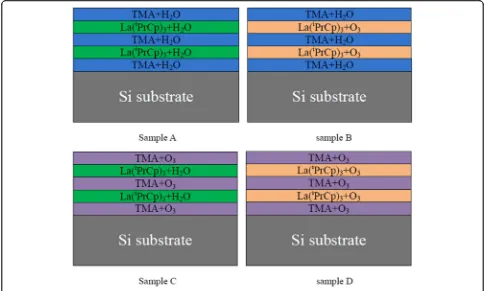
(RTA). Figure 1 shows the schematic drawings of struc-tures of different LaxAlyO films. The number of
depos-ition cycles for all films were 100. Film thicknesses were measured by J.A. Woollam M2000D spectroscopic ellipso-metry. The bonding structures of the films were examined by X-ray photoelectron spectroscopy (XPS). The electrical properties of the films were measured using a metal-insulator semiconductor (MIS) capacitor structure. Metal gate (200 nm Au) with a diameter of 130 μm was de-posited by magnetron sputtering through a shadow mask, and Al was sputtered as the back contact metal. Capacitance-voltage (C-V) characteristics were evalu-ated using an Agilent B1500A semiconductor param-eter analyzer. The EOT and dielectric constant of the capacitor were obtained by the Hauser CVC program taking into account quantum mechanical effects.
Results and Discussion
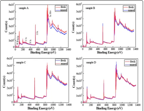
Figure 2 shows the XPS spectra of the LaxAlyO films
with different oxidants before and after annealing. The main peaks consist of Al 2p, O 1 s, and La 3d5/2peaks;
subordinate peaks consist of C 1 s, N 1 s, and Si 2p peaks. The interactions between La2O3and Al2O3layers
occur, which is accompanied with the decomposition and recomposition of unstable bonds or groups residing in LaxAlyO films during the annealing process.
There-fore, the change is observed in the XPS spectrum of the LaxAlyO films after annealing. On the other hand, an
ob-vious change is observed in the spectrum of sample A after annealing compared to the other samples. This phenomenon attributed to the physical adsorption prop-erty of H2O. The high-concentration hydroxyl/hydrogen
groups were formed in LaxAlyO films although the purge
time is sufficiently long during the ALD process. The residue of hydroxyl/hydrogen groups generated many defects and dangling bonds, which causes the increasing of the impurity residuals in LaxAlyO films. In contrast to
the H2O, O3 preserves the self-limiting nature of ALD
reactions, and no oxidant by-products reside in film growth. Therefore, the change is not obvious in the spectrum of sample D after annealing.
The XPS quantitative analysis is performed to deter-mine the chemical composition of the film. Figure 3 shows the percentage compositions of C and N impur-ities for LaxAlyO films. The residual C impurity mainly
as-deposited samples. In Fig. 3a, the percentage compos-ition of C impurity for as-deposited sample A is higher than that for the other samples. Moreover, the variation of the degree of reduction of the percentage composition of C impurity for sample A is more severe than that for the other samples after annealing. This result indicates that the film using O3as an oxidant is more prone to
achieve the saturation adsorption reaction and has a greater advantage in controlling the C impurity level compared with the film using H2O as an oxidant [19].
On the other hand, the percentage composition of N im-purity for as-deposited sample D is higher than that for the other samples shown in Fig. 3b. The residual N im-purity mainly comes from the formation of La–N and Si–N bonding. O3 with strong oxidization and lability
can split the N–C bonds of by-products and ligands easily. The unsaturated dangling bonds attach to La in the de-position process and form La–N bonds, which is defined as residual N-related impurities. Due to the diffusivity of the atoms, furthermore, Si–N bonds are formed at the interface between the film and Si substrate in the depos-ition process. The two reasons explain the phenomenon that the percentage composition of N impurity of sample D is higher than that of the other samples. During the an-nealing process, the unstable bonds can decompose, and carrier gas purges the residue out of the chamber which caused the decreasing of the content of N impurity [22].
Table 1 shows the percentage compositions of different atoms in different LaxAlyO films. The ratio of La:Al:O
approximately 1:3:6 for each samples before and after annealing indicates that the oxidants have a small influ-ence on the stoichiometry of LaxAlyO films. In
conclu-sion, the LaxAlyO film grown with O3 as the oxidant
generates lower C and higher N impurity level than the films using H2O as an oxidant. C and N impurity
con-centrations decreased, and the characteristics of LaxAlyO
films improved after rapid thermal annealing.
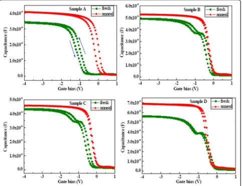
Figure 4 shows C-V characteristics of the LaxAlyO
films with different oxidants before and after annealing. The gate voltage was swept from negative to positive voltage and then again back to negative voltage. C-V curves with O3 used as oxidant formed a width step
which is caused by the trapped holes injected from the LaxAlyO layer into the depletion layer. The width of the
depletion layer in the Si substrate grows with the gate bias increasing. Growth of the depletion layer will stop, and the capacitance becomes constant after all the trapped holes in the interface layer are injected into the depletion layer. Magnitude of the trap charge concentra-tion in the oxide layer is determined by the magnitude of the hysteresis voltage. Sample D has a small hysteresis voltage compared with the other samples before anneal-ing. This indicates that film using O3as an oxidant
pos-sesses low-interface state density and good-interface
[image:3.595.55.539.88.379.2]quality. For samples A, B, and C, oxidant contains water, and the complex interface layer (IL) is formatted due to the interdiffusion of Si, Al, La, and O atoms in the deposition process. Moreover, the values of flat band voltage (VFB) of four samples are negative before
an-nealing. This attributed to the formation of positive
fixed charges in films. The formation of oxygen va-cancies in LaxAlyO films increases the positive oxide
charge due to the growth of silicate interfacial layer. The flat band voltage was shifted in a positive direc-tion, and the hysteresis voltages decreased after an-nealing at 600 °C for LaxAlyO films. The quantity of
Fig. 2XPS spectra of LaxAlyO films grown using different oxidants before and after annealing
[image:4.595.56.542.87.464.2] [image:4.595.58.540.586.715.2]positive charges is reduced, and oxygen vacancies are filled due to the decomposition and recombination of chemical bonds in films during the annealing process [23]. This indicates that LaxAlyO films possess a
lower trap charge density and a better quality after annealing.
On the other hand, the values of accumulation capaci-tance of films increased after annealing; this attributed to a decrease of the concentration of interfacial fixed charge and defects. However, sample D has a large value of accumulation capacitance compared with the other samples before and after annealing. There are two rea-sons for this phenomenon. First of all, films deposited with oxidant containing H2O tend to easily form
La(OH)3 which will decrease the whole dielectric
con-stant and value of accumulation capacitance of films. Secondly, the use of O3 as the oxidant improved
elec-trical properties of the LaxAlyO films by suppressing the
formation of complex interfacial layers and La(OH)3[24].
Figure 5 shows the values of thickness of the LaxAlyO
films. The values of thickness of samples B and D are higher than the values of thickness of samples A and C. This indicates that the growth rates of La2O3and Al2O3
films using O3 as an oxidant are higher than the films
using H2O as an oxidant. Growth rates of Al2O3 films
[image:5.595.57.290.110.236.2]achieved stable values of 0.97 and 1.01 Å/cycle when
Table 1Percentage compositions of atomic atoms in LaxAlyO films
Sample La(at%) Al(at%) O(at%) C(at%) N(at%) Sample A Fresh 11.99 26.37 56.35 3.58 1.71
Anneal 11.28 27.14 57.48 2.64 1.46
Sample B Fresh 11.96 26.69 57.24 2.79 1.32
Anneal 9.98 27.18 59.15 2.55 1.14
Sample C Fresh 11.24 26.04 57.69 3.41 1.62
Anneal 11.03 26.58 58.17 2.85 1.37
Sample D Fresh 9.75 27.17 58.61 1.83 2.64
Anneal 8.91 27.78 59.87 1.51 1.93
[image:5.595.58.541.344.716.2]H2O is used as oxidant, and growth rates of La2O3films
achieved stable values of 0.71 and 1.03 Å/cycle when O3
is used as oxidant. This result indicates that the film using O3 as an oxidant is more prone to achieve the
saturation adsorption reaction. This analysis is in accord with the analyses of changes of impurity content we discussed before. Furthermore, the values of thickness of the LaxAlyO films increased after annealing because of
the formation of an interfacial layer between the film
growth layer and Si substrate. Moreover, the change of values of thickness of four LaxAlyO films before and after
annealing is negligible. This can be explained by the densi-fication of the films after thermal annealing [25].
Figure 6 shows the values of dielectric constant and EOT of the LaxAlyO films. As shown in Fig. 6, thekvalue
and EOT of sample A are 10.7 and 5.8 nm, respectively. Sample A has a small permittivity and large EOT com-pared with the other samples. The small permittivity
Fig. 5Values of thickness of the LaxAlyO films before and after annealing
[image:6.595.58.538.87.328.2] [image:6.595.57.538.488.709.2]attributed to the formation of La(OH)3 and La silicate
during the ALD process. Formation of much La(OH)3is
because of the reaction of La2O3layer and the moisture
contained in H2O oxidant, carrier gas, and atmosphere
[26]. Formation of La silicate attributed to the interdiffu-sion of La and O atoms that belong to La2O3layer close
to substrate and Si atoms which came from Si substrate. The kvalue and EOT are 18.1 and 3.6 nm of sample D, which has the largest permittivity and smallest EOT. This phenomenon attributed to the advantage of O3. Different
from H2O, the use of O3as an oxidant can suppress the
formation of La(OH)3. This caused sample D possessing
large permittivity. Values of EOT andkvalue of sample B are 4.2 nm and 15.1, respectively; values of EOT and k value of sample C are 4.6 nm and 13.5, respectively. For the two samples, both with mixed as oxidants, possess dif-ferent properties. For sample C, the La precursor reacts with O3 while the Al precursor reacts with H2O in the
deposition process. For sample B, on the contrary, the La precursor reacts with H2O, while the Al precursor reacts
with O3. The different deposition sequences of oxidants
for H2O and O3cause sample C formatting less La(OH)3
and better interface layer quality which attributed to the reaction of saturated adsorption in La2O3 films and less
diffusion between atoms at interface compared with B. The phenomenon makes sample C possessing larger permittivity and smaller EOT than sample B.
EOT decreased and permittivity increased of the four samples after annealing at 600 °C. The reduction of EOT mainly attributed to the densification process of LaxAlyO
films. The La, Si, and O atoms recombined in interface layer during the RTA process; this caused a decrease of the concentration of interfacial fixed charge and defects [27]. Furthermore, the increasing of permittivity attrib-uted to the increasing of accumulation capacitance and reduction of impurity after annealing.
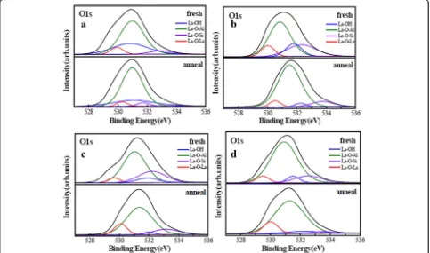
In order to prove the analyses above, XPS spectra were obtained using Al Kα. The binding energy (BE) was cali-brated with the position of the C 1 s peak at 284.8 eV. O 1 s spectrums of four samples before and after annealing were fitted with four peaks after the application of a Smart background are shown in Figure 7. Red, green, blue, and purple curves stand for the La–O–La, La–O– Al, La–OH, and La–O–Si bonds, respectively. The exist-ence of La–O–Al and La–O–La bonds attributed to the formation of LaxAlyO and La2O3 layer in films. The
existence of La–O–Si bond indicates the formation of La silicate at La2O3/Si interfacial layer [28]. According
to previous report, La atom has the strongest tendency among rare earth atoms forming silicate components [29]. Thus, the first few cycles of ALD La2O3 are
con-sumed to form a silicate interlayer. As shown in Fig. 7a, sample A possesses a large intensity of La–OH peak which attributed to the La(OH)3 compared with the
[image:7.595.57.540.427.712.2]other samples. This phenomenon indicates that the film with H2O used as oxidant more easily leads to the
for-mation of La hydroxide and reduction of permittivity. As shown in Fig. 7b, c, the intensities of La–OH and La–O–Si peaks of sample B are larger than that of sam-ple C. This difference indicates that samsam-ple B has a large EOT and a small permittivity compared with sample C, which coincides with the values of EOT and permittivity for corresponding samples.
Moreover, the intensities of La–OH and La–O–Si peaks of LaxAlyO films decreased after annealing at
[image:8.595.305.539.244.742.2]600 °C. This attributed to the reduction of impurity con-tent and concentration of defects in the interface of films during the annealing process. Sample D has a smallest intensity of La–OH and La–O–Si peaks com-pared with the other samples after annealing shown in Fig. 7d. This indicates that the use of O3as the oxidant
suppressed the formation of La(OH)3 and growth of
interface layer. To summarize, annealing improved the electrical properties and increased the permittivity of LaxAlyO films.
Conclusions
In summary, the annealing effect of LaxAlyO
nanolami-nate films with different oxidants (H2O and O3)
depos-ited on a Si substrate by ALD was investigated. First of all, the C and N impurity concentrations in LaxAlyO
films were improved by rapid thermal annealing. More-over, electrical properties were improved of films, and content of La hydroxide was reduced by rapid thermal annealing, which makes films to have a large dielectric constant and a small EOT. Furthermore, the use of H2O
as the oxidant leads to the formation of La(OH)3, which
makes the properties of films worse. Using O3 as the
oxidant improved electrical properties of the deposited LaxAlyO films by suppressing the formation of interface
layer and La(OH)3. The LaxAlyO film using O3 as an
oxidant possessed a high permittivity and a small EOT compared with the other samples after annealing. These results show that using O3 as an oxidant is suitable for
high-performance ALD LaxAlyO film deposition as
required for gate dielectric applications.
Abbreviations
ALD:Atomic layer deposition; CMOS: Complementary metal-oxide-semiconductor; EOT: Equivalent oxide thickness; IL: Interfacial layer; La(iPrCp)
3: Tris(isopropylcyclopentadienyl) lanthanum; MBE: Molecular beam
epitaxy; MIS: Metal-insulator semiconductor; MOCVD: Metal-organic chemical vapor deposition; PDA: Post-deposition annealing; PLD: Pulsed laser deposition; RTA: Rapid thermal annealing; TMA: Trimethylaluminum; XPS: X-ray
photoelectron spectroscopy
Acknowledgements
This research is supported by the National Natural Science Foundation of China (Grant Nos. 61376099 and 61434007) and the Foundation for Fundamental Research of China (Grant No. JSZL2016110B003).
Authors’Contributions
CxF generated the research idea, analyzed the data, and wrote the paper. CxF and XW carried out the experiments and measurements. XyF and LZ participated in the discussions. HxL has given final approval of the version to be published. All authors read and approved the final manuscript.
Competing Interests
The authors declare that they have no competing interests.
Publisher’s Note
Springer Nature remains neutral with regard to jurisdictional claims in published maps and institutional affiliations.
Received: 25 December 2016 Accepted: 12 March 2017
References
1. Gray NW, Prestgard MC, Tiwari A (2014) Tb2O3thin films: an alternative
candidate for high-k dielectric applications. Appl Phys Lett 105:222903 2. Wong H, Yang BL, Dong S, Iwai H, Kakushima K, Ahmet P (2012) Current
conduction and stability of CeO2/La2O3stacked gate dielectric. Appl Phys
Lett 101:233507
3. Terlinden NM, Dingemans G, Vandalon V, Bosch RHEC, Kessels WMM (2014) Influence of the SiO2interlayer thickness on the density and polarity of
charges in Si/SiO2/Al2O3stacks as studied by optical second-harmonic
generation. J Appl Phys 115:033708
4. Cao D, Cheng X, Jia T, Xu D, Wang Z, Xia C et al (2013) Characterization of HfO2/ La2O3layered stacking deposited on si substrate. J Vac Sci Technol B
31:01A113
5. Sharma A, Longo V, Verheijen MA, Bol AA, (Erwin) Kessels WMM. Atomic layer deposition of HfO2using HfCp(NMe2)3and O2plasma. J. Vac. Sci.
Technol. A. 2017; 35:01B130
6. Weinreich W, Wilde L, Müller J, Sundqvist J, Erben E, Heitmann J et al (2013) Structural properties of as deposited and annealed ZrO2influenced by atomic
layer deposition, substrate, and doping. J Vac Sci Technol A 31:257–264 7. Wang X, Liu HX, Fei CX, Yin SY, Fan XJ (2015) Silicon diffusion control in
atomic-layer-deposited Al2O3/La2O3/Al2O3gate stacks using an Al2O3barrier
layer. Nanoscale Res Lett 10:141
8. Chu RL, Chiang TH, Hsueh WJ, Chen KH (2014) Passivation of GaSb using molecular beam epitaxy Y2O3to achieve low interfacial trap density and
high-performance self-aligned inversion-channel p-metal-oxide-semiconductor field-effect-transistors. Appl Phys Lett 105:182106 9. Cheng S, Sang L, Liao M, Liu J, Imura M, Li H et al (2012) Integration of
high-dielectric constant Ta2O5oxides on diamond for power devices. Appl
Phys Lett 101:232907
10. Yan Z, Zhou C, Xiang Z, Peng Z, Dou Y, Wang W et al (2013) Passivation mechanism of thermal atomic layer-deposited Al2O3films on silicon at
different annealing temperatures. Nanoscale Res Lett 8:114 11. Zhang X, Tu H, Zhao H, Yang M, Wang X, Xiong Y et al (2011) Band
structure and electronic characteristics of cubic La2O3gate dielectrics
epitaxially grown on InP substrates. Appl Phys Lett 99:132902 12. Mcdonnell S, Pirkle A, Kim J, Colombo L, Wallace RM (2012)
Trimethyl-aluminum and ozone interactions with graphite in atomic layer deposition of Al2O3. J Appl Phys 112:104110
13. Suzuki M, Yamaguchi T, Fukushima N, Koyama M (2008) LaAlO3gate
dielectric with ultrathin equivalent oxide thickness and ultralow leakage current directly deposited on Si substrate. J Appl Phys 103:034118 14. Zhang HT, Dedon LR, Martin LW, Engelherbert R (2015) Self-regulated
growth of LaVO3thin films by hybrid molecular beam epitaxy. Appl Phys
Lett 106:233102
15. Golalikhani M, Lei QY, Chen G, Spanier JE, Ghassemi H, Johnson CL et al (2013) Stoichiometry of LaAlO3films grown on SrTiO3by pulsed laser
deposition. J Appl Phys 114:027008
16. Yeluri R, Liu X, Guidry M, Koksaldi OS, Lal S, Kim J et al (2014) Dielectric stress tests and capacitance-voltage analysis to evaluate the effect of post deposition annealing on Al2O3films deposited on GaN. Appl Phys Lett 105:222905
17. Lim BS, Rahtu A, Gordon RG (2003) Atomic layer deposition of transition metals. Nat Mater 2:749–54
18. Batra N, Gope J, Vandana N, Panigrahi J, Singh R, Singh PK (2015) Influence of deposition temperature of thermal ALD deposited Al2O3films on silicon
19. Park TJ, Sivasubramani P, Coss BE, Kim HC, Lee B, Wallace RM et al (2010) Effects of O3and H2O oxidants on C and N-related impurities in
atomic-layer-deposited La2O3films observed by in situ x-ray photoelectron
spectroscopy. Appl Phys Lett 97:092904
20. Yao Y, Fu K, Yan C, Dai J, Chen Y, Wang Y, Zhang B, Hitz EM, Hu L (2016) Three-dimensional printable high-temperature and high-rate heaters. ACS Nano 10:5272–5279
21. Ma JW, Lee WJ, Cho M-H, Chung KB, An C-H, Kim H, Cho YJ, Moon DW, Cho HJ (2011) Changes in electronic structure of LaxAlyO films as a function of
postdeposition annealing temperature. J Electrochem Soc 158:G79–G82 22. Fan JB, Liu HX, Ma F, Zhuo QQ, Hao Y (2013) Influences of different oxidants
on the characteristics of HfAlOxfilms deposited by atomic layer deposition.
Chinese Phys B 22:027702
23. Cao D, Cheng X, Zheng L, Wang Z (2014) Effects of rapid thermal annealing on the properties of HfO2/La2O3nanolaminate films deposited by plasma
enhanced atomic layer deposition. J Vac Sci Technol A 33:01A116 24. Lee B, Park TJ, Hande A, Kim MJ, Wallace RM, Kim J et al (2009) Electrical
properties of atomic-layer-deposited La2O3films using a novel La
formamidinate precursor and ozone. Microelectron Eng 86:1658–1661 25. Eom D, Hwang CS, Kim HJ, Cho MH, Chung KB (2008) Thermal annealing
effects on the atomic layer deposited LaAlO3thin films on Si substrate.
Electrochem Solid-State Lett 11:7
26. Suzuki M (2012) Comprehensive study of lanthanum aluminate high-dielectric-constant gate oxides for advanced CMOS devices. Materials 5:443–477 27. Molina J, Tachi K, Kakushima K, Ahmet P, Tsutsui K, Sugii N et al (2007)
Effects of N2-based annealing on the reliability characteristics of tungsten/
La2O3/silicon capacitors. J Electrochem Soc 154:G110–G116
28. Maeng WJ, Kim WH, Kim H (2010) Flat band voltage (VFB) modulation by
controlling compositional depth profile in La2O3/HfO2nanolaminate gate
oxide. J Appl Phys 107:074109
29. Chiang CK, Wu CH, Liu CC, Lin JF, Yang CL, Wu JY et al (2011) Effects of La2O3capping layers prepared by different ALD lanthanum precursors on
flatband voltage tuning and EOT scaling in TiN/HfO2/SiO2/Si MOS structures.
J Electrochem Soc 158:H447–H451
Submit your manuscript to a
journal and benefi t from:
7Convenient online submission
7Rigorous peer review
7Immediate publication on acceptance
7Open access: articles freely available online
7High visibility within the fi eld
7Retaining the copyright to your article