N A N O R E V I E W
Open Access
Formation mechanisms of nano and microcones
by laser radiation on surfaces of Si, Ge, and SiGe
crystals
Artur Medvid
1,2*, Pavels Onufrijevs
1, Renata Jarimaviciute-Gudaitiene
3,4, Edvins Dauksta
1and Igoris Prosycevas
3Abstract
In this work we study the mechanisms of laser radiation interaction with elementary semiconductors such as Si and Ge and their solid solution SiGe. As a result of this investigation, the mechanisms of nanocones and microcones formation on a surface of semiconductor were proposed. We have shown the possibility to control the size and the shape of cones both by the laser. The main reason for the formation of nanocones is the mechanical compressive stresses due to the atoms’redistribution caused by the gradient of temperature induced by strongly absorbed laser radiation. According to our investigation, the nanocone formation mechanism in semiconductors is characterized by two stages. The first stage is characterized by formation of a p-n junction for elementary semiconductors or of a Ge/Si heterojunction for SiGe solid solution. The generation and redistribution of intrinsic point defects in elementary semiconductors and Ge atoms concentration on the irradiated surface of SiGe solid solution in temperature gradient field take place at this stage due to the thermogradient effect which is caused by strongly absorbed laser radiation. The second stage is characterized by formation of nanocones due to mechanical plastic deformation of the compressed Ge layer on Si. Moreover, a new 1D-graded band gap structure in elementary semiconductors due to quantum confinement effect was formed. For the formation of microcones Ni/Si structure was used. The mechanism of the formation of microcones is characterized by two stages as well. The first stage is the melting of Ni film after irradiation by laser beam and formation of Ni islands due to surface tension force. The second step is the melting of Ni and subsequent manifestations of Marangoni effect with the growth of
microcones.
Keywords:Laser radiation, Microcones, Nanocones, Thermogradient effect
Review
Introduction
Semiconductor nanostructures are the most investigated object in solid state physics due to their promising appli-cation in microelectronics and optoelectronics. Today we have some well-developed methods for the formation of nanostructures: MBE [1], CVD [2], ion implantation [3], and laser ablation [4]. The above-mentioned methods need subsequent thermal annealing of the structures in a furnace. Nanostructure growths by these methods need a lot of time and a high-vacuum or a special environment,
for example, inert Ar gas. As a result, nanocrystals grow with uncontrollable parameters, broad size distribution, and chaotically, the so-called self-assembly. Therefore, one of the important tasks for nanoelectronic and optoelec-tronic growth is the elaboration of new methods for the formation of nanostructures in semiconductors with con-trolled features.
On the other hand, laser technology is of interest both fundamentally because laser radiation of a semiconduc-tor can lead to different and sometimes opposite results, for example, annealing defects after ion implantation or creating new additional defects and from a device view-point [5], since it can be used for annealing B/n-Si or F/p-Si structures during p-n junction formation which is appropriate for many kinds of microelectronic de-vices [6].
* Correspondence:[email protected]
1
Institute of Technical Physics, Riga Technical University, 14 Azenes Str, Riga, Latvia
2
Institute of Semiconductor Physics, NAS of Ukraine, 45 Pr. Nauki, Kyiv, Ukraine
Full list of author information is available at the end of the article
Moreover, our recent investigations have shown that laser radiation can be successfully applied for formation of cone-like nanostructures [7-10] with laser intensity, which do not cause melting of the material. The 1D-graded band gap structure in elementary semiconductors was formed due to quantum confinement effect [8]. Fur-thermore, it has been shown that irradiation by laser of Si single crystal with intensity which exceeds melting of material leads to formation of microcones, which are possible to use for solar cells, the so-called black Si [11]. The lack of understanding of the interaction effects of laser radiation with a semiconductor limits laser tech-nology application in microelectronics [12]. So the aims of this research are to show a new possibility for for-mation of nanocones and microcones on a surface of elementary semiconductors (Si, Ge) and their solid solu-tion by laser radiasolu-tion, and to propose the mechanism of cones formation.
Materials and methods
For the formation of nanocones in the experiments on i-type Ge single crystals with resistivity ρ = 45 Ω cm,
Na = 7.4 × 1011 cm−3, Nd = 6.8 × 1011cm−3, where Na andNdare acceptor and donor concentrations, and sam-ples with the size of 16.0 × 3.0 × 2.0 mm3 were used. The samples were mechanically polished with diamond paste and chemically treated with H2O2and CP-4 (HF/ HNO3/CH3COOH in volume ratio of 3:5:3).
Different intensities, pulse durations, and wavelengths of nanosecond Nd:YAG laser were used to irradiate the samples (pulse repetition rate at 12.5 Hz, power of
P = 1.0 MW and wavelength of λ = 1,064 nm). The diameter of the spot of the laser beam was 3 mm, and point-to-multipoint method was used for irradiation of the samples. All experiments of nanocone formation were performed in ambient atmosphere at pressure of 1 atm,T = 20°C, and 60% humidity. Current–voltage (I-V)
characteristics were measured for the nonirradiated and irradiated samples with nanocones formed on a surface of i-Ge samples. The measurements of theI-V character-istics were performed by soldering 99% tin and 1% an-timony alloy contacts directly on the irradiated surface of Ge with the tin contacts on the opposite side. Mea-surements of I-V characteristics were done at room temperature and atmospheric pressure.
The structure consisting of Ni catalyst with thick-nesses d= 30 nm deposited on commercial Si(111) sin-gle crystals were used for formation of microcones. Pulsed Nd:YAG laser for treatment Ni/Si structure with following parameters was used: wavelength ofλ = 1,064 nm, pulse duration of τ= 150 ms, pulse repetition rate of 12.5 Hz, power atP= 1.0 MW, laser intensity ofI= 4 MW/cm2. The threshold intensity of microcones forma-tion is 3.15 MW/cm2. The samples were treated by laser radiation in scanning mode with step of 20 μm. All ex-periments of microcones formation were performed in ambient atmosphere at pressure of 1 atm,T = 20°C, and 60% humidity.
Investigations of the reflection obtained from the sur-face with decorated microcones structure were done with Avantes AvaSpec-2048 UV/VIS/NIR spectrometer (Avantes Inc., Apeldoorn, The Netherlands) in the wave-length range of 200 to 1,100 nm [spectrometer based on AvaBench-75 symmetrical Czerny-Turner construction (Avantes Inc., Apeldoorn, The Netherlands) with 2,048 pixel CCD detector and resolution of 1.4 nm].
[image:2.595.59.539.556.706.2]Surface morphology and chemical analysis of the sam-ples by scanning electron microscope (SEM) with inte-grated energy dispersive X-ray spectrometer (SEM-EDX) Hitachi S-900 (Hitachi America, Ltd., Brisbane, CA, USA) were used. Photoluminescence (PL) measurements were performed by equipment Fluorolog-3, using photo detector Hamamatsu R928 and xenon lamp (450 W) (Hamamatsu Photonics GmbH, Herrsching, Germany).
Results and discussion
Nanocones
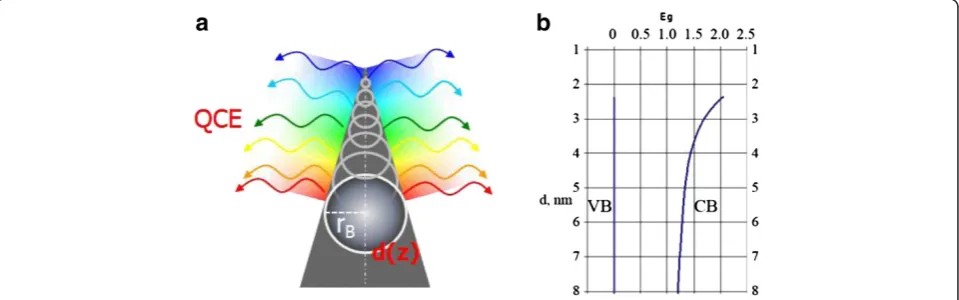
Quantum confinement effect (QCE) is one of the most investigated phenomena in semiconductors. The pre-sence of QCE in semiconductors leads to a crucial change of physical properties of the material, especially in quantum dots. Recently, a new quantum system, quantum cone [9], which possesses unique properties, was observed. It is known that if the radius of the sphere inscribed in nanostructure is equal or less than Bohr’s radius of exciton, quantum confinement effect takes place [13]. The diameter of the nanocone is a function
of its heightd(z); therefore, a nanocone is a graded band gap structure. A schematic image of a nanocone with a gradually increasing band gap from a substrate up to the tip of the cone is shown in Figure 1a. A calculated band gap structure of Si as a function of the nanowire’s diameter using the formula from the paper [14] ΔEg =
(2Ћ2ζ2) / (m*d2), where 1/ (m*)=1 / (me*)+ 1 / (mh*),
(me* and mh*are electron and hole effective masses,
re-spectively) andd is the diameter, is shown in Figure 1b. For QWs, ζ = 2.4048. In our case, the diameter of the nanocone is a function of its height d(z); therefore, it is a graded band gap semiconductor. The shape of this quantum structure allows us to obtain graded band gap in elementary semiconductors. The physical properties of a semiconductor strongly depend on the solid angle of the nanocone. So if the angle is about 60°, then the nanocone is a quantum dot - 0D system; if the angle tends to be at 180°, then the nanocone degenerates to a quantum well - 2D system; and if the angle tends to 0°, then the nanocone degenerates to the wire - 1D system. The most interesting case is when the angle is between 60° and 0°, then band gap of a semiconductor gradually increases towards the top of the nanocone, leading to a graded band gap structure. The possibility of wide appli-cations of graded band gap structure in optoelectronics devices was shown in [12]. For example, a photodetector possessing both properties can be of bolometric type with an ‘open window’ on top of the cones or with a selective spectral sensitivity depending on light propa-gation direction and a light source with gradual change of the emitted wavelength depending on z-coordinate.
-3.0 -2.5 -2.0 -1.5 -1.0 -0.5 0.0 0.5 1.0 1.5 2.0
-0.002 0.000 0.002 0.004 0.006 0.008 0.010 0.012 0.014 0.016 0.018 0.020
I, A
U, V 1
[image:3.595.57.290.89.247.2]2
Figure 2Current–voltage characteristics of Ge sample and plot ofd(V) /d(lnJ) andH(J).I-Vcharacteristics (curve 1) before and after irradiation (curve 2) by Nd:YAG laser at intensityI= 1.15 MW/cm2
and wavelengthλ= 266 nm. (1, A) Plot ofd(V) /d(lnJ) andH(J) depending on current densityJaccording to [21].
[image:3.595.60.538.473.714.2]Understanding of the mechanism of nanocones forma-tion in semiconductors by laser radiaforma-tion is a very im-portant task for physics and nanotechnology. Recently, we have shown a possibility to form nanocones by Nd: YAG laser radiation on the surface of elementary semi-conductors such as Si [8], Ge [7], and CdZnTe [13], and SiGe [9] solid solutions. The phenomena of ‘blue shift’ of the PL spectra and ‘red shift’ of the phonon LO line in the Raman spectra are explained by exciton and pho-non quantum confinement effect in nanocones [7]. The asymmetry of the PL band in the spectrum of Si nanocones is explained by the formation of 1D-graded band gap structure [8]. A two-stage mechanism of nanocones formation has been proposed for SiGe solid solution [9]. The first stage of nanocones formation is the generation and redistribution of point defects (impurity atoms and intrinsic defects - vacancies and in-terstitials) in temperature gradient field, the so-called thermogradient effect (TGE) [15]. As a result of TGE, a new phase on the irradiated surface is formed, for ex-ample, Ge phase on the surface of SiGe solid solution [9], which was confirmed by appearance of new LO line in back-scattering Raman spectra. The second stage is characterized by mechanical plastic deformation of the strained top layer leading to arise of the nanocones due to selective laser absorption of the top layer. This stage is more or less similar to Stranski-Krastanov (S-K) growth mode of quantum dots. The main difference be-tween the processes is the nonhomogeneous heating up of the structure. In the S-K mode, heating in ho-mogenous temperature field takes place, but in the case of laser heating, most of the energy of laser radiation is absorbed by the top layer. Therefore, control of na-nocones parameters by laser intensity, wavelength, and number of pulses is possible, as was shown on SiGe solid solution [9]. The first stage is more difficult for under-standing of the physical processes which take place
[image:4.595.55.539.89.246.2]during of growth of nanocones, especially in pure intrin-sic elementary semiconductors (Ge, Si) and compounds (GaAs, CdTe). It is clear now that the key step in both S-K growth mode and nanocone laser growth technol-ogy is the formation of mechanically strained layers. For elementary semiconductors, such as Si and Ge crystals, mechanical stress already exists due to p-n junction for-mation, which depends on doping level and effective diameter of the impurities in the atoms. Moreover, the possibility to form p-n junction in p-Si [16-18] and p-Ge [19] by strongly absorbed laser has been shown. We propose the following mechanism of nanocones forma-tion in pure elementary semiconductor: at the first stage, generation and redistribution of intrinsic point defects in temperature gradient field do occur. The redistribu-tion of defects takes place because interstitial atoms drift towards the irradiated surface, but vacancies drift in the opposite direction - in the bulk of semiconductor ac-cording to the thermogradient effect. Since the intersti-tials in Ge crystal are of n-type and vacancies are known to be of p-type [20], a p-n junction is formed. I-V char-acteristics after irradiation by Nd:YAG laser at intensity Figure 4Dynamics of nanocones formation by laser radiation in intrinsic semiconductors.(1–8) Schematic images of dynamics of
nanocones formation by laser radiation in intrinsic semiconductors.
[image:4.595.304.539.569.689.2]I = 1.15 MW/cm2 and wavelength λ = 266 nm are an evidence of the first stage in i-Ge (Figure 2, curve 2). According to the calculations the ideality factor,n is in-creasing from 2.2 to 20 as the current increases, and the potential barrier height isΦ= 1.1 eV. We explained that such potential barrier height by the formation of he-terojunction due to quantization of electron energy in the top layer cannot exceed the band gap of Ge crystal
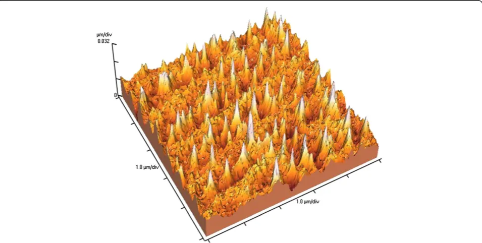
(0.67 eV at room temperature). An evidence of this sug-gestion is the absence of photovoltaic force on the po-tential barrier. The large ideality factor can be explained by the additional resistivity caused by large thickness of the crystal at approximately 1 mm and by deep level (Ea = 0.2 eV) of vacancies as a p-type impurity [20]. At the second stage of the process, nanocones (Figure 3) are formed on the irradiated surface of the semiconduc-tors due to plastic deformation of the top layer (n-type) in the same way as in the previous case with semicon-ductor solid solutions. Dynamics of nanocones forma-tion by laser radiaforma-tion in intrinsic semiconductors is shown in Figure 4.
Microcones
It is known that microcones of Si can absorb more than 95% of incident light [22] because in array of micro-cones, light is repeatedly reflected between the mi-crocones and is absorbed almost completely, and a single Si crystal reflects visible light by 30% [23]. The microstructured surface is completely black to the naked eye (see Figure 5). Therefore, Si with microcones is known as black Si [24]. Black Si is an excellent material for solar cells [22]. Solar cells with microcones are proved to be more efficient, generating more current than the conventional one. Also, black Si can be used to make infrared detectors, which is a new application for Si [24].
[image:5.595.56.291.90.578.2]The surface microstructuring of ordinary Si by pulsed femtosecond laser-induced plasma [25,26] or chemical vapor deposition with catalytic metal on Si [27] is used for black Si formation. We proposed a new laser me-thod, which is simpler and cheaper comparison with above-mentioned methods [11].
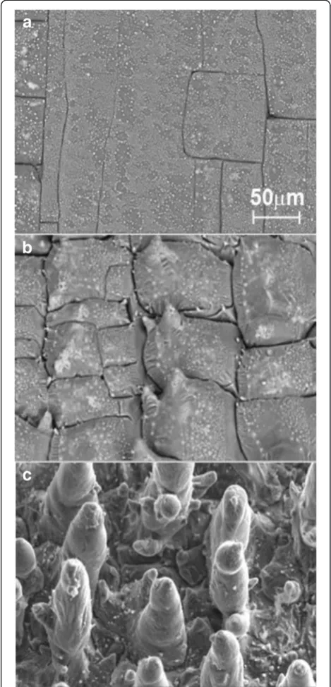
Figure 6SEM images of Ni/Si surface irradiated by Nd:YAG laser.SEM images of Ni/Si surface irradiated by Nd:YAG laser at intensity 4.5 MW/cm2: 3 laser pulses per point (a), 10 laser pulses per point (b), and 22 laser pulses per point (c).
Figure 7SEM image of Ni/Si surface irradiated by Nd:YAG laser.
[image:5.595.305.539.521.694.2]In our experiments, after Ni/Si structure irradiation by Nd:YAG laser, various degrees of damage are observed on the surface of the Ni/Si, such as the appearance of cracks and formation of small (several microns) Ni islands, as shown in Figure 6a. The Nd:YAG laser inten-sity threshold, at which the self-organization of cone-like microstructures with the size of 3.15 MW/cm2, was ob-served on the surface of Ni/Si layer system. The further increase of the laser intensity and number of pulses lead to the formation of cone-like microstructures and ma-ximal height of the cone of about 100 μm. The control
of the microcone shape and height was achieved by changing the intensity of laser radiation and a number of pulses (Figure 6b,c) [11].
Optical reflection measurements showed that the inte-grated reflection of black Si is by 97.73% lower than for crystalline wafer of Si (Figure 7). For example, in visible region of the spectra at 500 nm, the reflection from sili-con drops approximately from 35% to 1% after micro-cones formation.
We proposed a two-stage mechanism of microcones formation. The first stage is melting of Ni thin film after
200 400 600 800 1000
0.01 0.1 1 10 100
Ref
lection, %
Wavelenght, nm 1
2
[image:6.595.59.539.90.298.2]3
Figure 8Reflection spectra of Si surface with microcones.The reflection spectra of Si: curve 1, Si single crystal; curves 2 and 3, Si with microcones formed by 1,600 and 2,000 number of the laser pulses, respectively. Angle of incidence is 90°.
400 450 500 550 600 650 700
0 20000 40000 60000 80000 100000 120000 140000 160000 180000 200000 220000
PL intensity, a.u.
Wavelength, nm
Lex = 340 nm
a
b
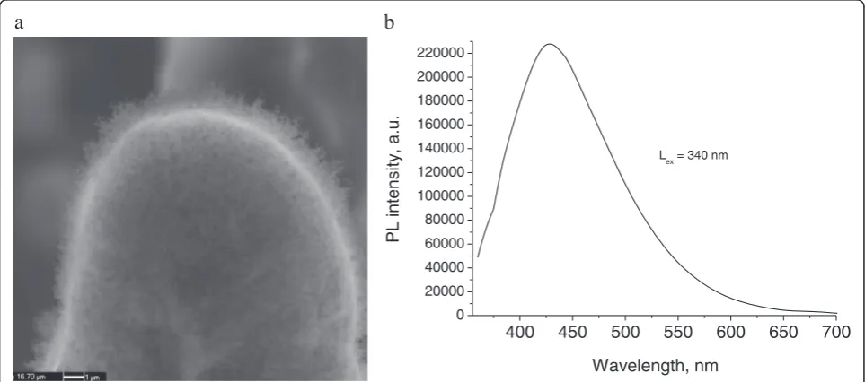
[image:6.595.57.539.492.705.2]irradiation by laser beam and formation of Ni islands due to surface tension force (Figure 8). The second stage is melting of the structure and mass transfer along an interface between two materials (Si and Ni islands) due to surface tension gradient, the so-called Marangoni effect [28]. Moreover, the detailed investigation of the morph-ology of single microcone using SEM has shown forma-tion of nanowires on the surface of microcone (Figure 9a). The EDX measurements showed a high content of oxygen atoms (54%) in the processed samples. In addition, a PL spectrum shows a wide band with maximum 430 nm (Figure 9b). From EDX and PL measurements it was pos-sible to conclude that nanowires consist of SiO2.
Conclusions
Based on the above results, the following conclusions can be drawn:
1. Experimentally, we have shown the possibility to control the size and the shape of cones both by the laser radiation and the semiconductor parameters. 2. Nanocone formation mechanism in semiconductors
is characterized by two stages. The first stage is characterized by formation of n-p junction for elementary semiconductors or Ge/Si heterojunction for SiGe solid solution. The second stage is
characterized by formation of nanocones due to mechanical plastic deformation of the compressed Ge layer on Si and in elementary semiconductor compressed n-type top layer.
3. The mechanism of the formation of microcones is characterized by two stages. The first stage is melting of Ni film after irradiation by laser beam and formation of Ni islands due to surface tension force. The second step is melting of Ni and
subsequent manifestations of Marangoni effect with growth of microcones.
Abbreviations
AFM:Atomic force microscope;I-V: current–voltage; PL: Photoluminescence; QCE: Quantum confinement effect; RR: Rectification ratio; SEM: Scanning electron microscope; S-K: Stranski-Krastanov; TGE: Thermogradient effect.
Competing interests
The authors declare that they have no competing interests.
Authors’contributions
AM conceived the studies and coordinated the experiment. All of the authors participated to the analysis of the data and wrote the article. PO and ED carried out the sample with nanocones preparation and characterization. RJG, ED, PO, and IP carried out the sample with microcones preparation and characterization. All the authors read and approved the manuscript.
Authors’information
AM is the head of Semiconductors Laboratory at Riga Technical University. PO is the lead researcher in Semiconductor Laboratory at Riga Technical University. ED is a Ph D student in Riga Technical University. RJG is an associate professor at Kaunas University of Applied Sciences. IP is an associate professor at Kaunas University of Technology.
Acknowledgments
Authors AM and PO gratefully acknowledge the financial support by the European Regional Development Fund within the project‘Sol–gel and laser technologies for the development of nanostructures and barrier structures’, 2010/0221/2DP/2.1.1.1.0/10/APIA/VIAA/145 and Latvian Council of Science according to the grant 10.0032.6.2. ED thanks for the support of this work by the European Social Fund within the project‘Support for the implementation of doctoral studies at Riga Technical University’. RJ thanks the Research Council of Lithuania for Postdoctoral fellowship that was funded by the European Union Structural Funds project‘Postdoctoral Fellowship Implementation in Lithuania.’
Author details
1
Institute of Technical Physics, Riga Technical University, 14 Azenes Str, Riga, Latvia.2Institute of Semiconductor Physics, NAS of Ukraine, 45 Pr. Nauki, Kyiv,
Ukraine.3Institute of Materials Science, Kaunas University of Technology, Savanoriu Ave. 271, Kaunas, Lithuania.4Faculty of Technology, Kaunas
University of Applied Sciences, Pramones Ave. 20, Kaunas, Lithuania.
Received: 28 March 2013 Accepted: 6 May 2013 Published: 4 June 2013
References
1. Talochkin AB, Teys SA, Suprun SP:Resonance Raman scattering by optical phonons in unstrained germanium quantum dots.Phys Rev2005,
72:115416–11154.
2. Wu XL, Gao T, Bao XM, Yan F, Jiang SS, Feng D:Annealing temperature dependence of Raman scattering in Ge+−implanted SiO2 films.J Appl Phys1997,82:2704.
3. Hartmann JM, Bertin F, Rolland G, Semeria MN, Bremond G:Effects of the temperature and of the amount of Ge on the morphology of Ge islands grown by reduced pressure-chemical vapor deposition.Thin Sol Film 2005,479:113–120.
4. Yoshida T, Yamada Y, Orii T:Electroluminescence of silicon
nanocrystallites prepared by pulsed laser ablation in reduced pressure inert gas.J Appl Phys1998,83:5427–5432.
5. Dumitras DC:Nd YAG Laser.Rijeka: InTech; 2012:318. ISBN 978-953-51-0105-5. 6. Shah RR, Hollingsworth DR, DeJong GA, Crosthwait DL:P-N junction and
Schottky barrier diode fabrication in laser recrystallized polysilicon on SiO2.Electron Device Lett, IEEE1981,2:159–161.
7. Medvid A, Dmytruk I, Onufrijevs P, Pundyk I:Quantum confinement effect in nanohills formed on a surface of Ge by laser radiation.Phys Status Solidi C2007,4:3066–3069.
8. Medvid A, Dmitruk I, Onufrijevs P, Pundyk I:Properties of nanostructure formed on SiO2/Si interface by laser radiation.Solid State Phenom2008,
131–133:559–562.
9. Medvid’A, Onufrijevs P, Lyutovich K, Oehme M, Kasper E, Dmitruk N, Kondratenko O, Dmitruk I, Pundyk I:Self-assembly of nanohills in Si1−
xGex/Si hetero-epitaxial structure due to Ge redistribution induced by laser radiation.J Nanosci Nanotechnol2010,10:1094–1098.
10. Medvid A, Mychko A, Pludons A, Naseka Y:Laser induced nanostructure formation on a surface of CdZnTe crystal.J Nano Res2010,11:107–112. 11. Medvid’A, Onufrijevs P, Dauksta E, Kyslyi V:“Black silicon”formation by
Nd:YAG laser radiation.Adv Mater Res2011,222:44–47.
12. Medvid’A:Chapter 2. Laser induced self-assembly nanocones’formation on a surface of semiconductors.InLaser Growth and Processing.Edited by Vainos N. London: Woodhead; 2012:85–112.
13. Medvid A, Mychko A, Strilchyk O, Litovchenko N, Naseka Y, Onufrijevs P, Pludonis A:Exciton quantum confinement effect in nanostructures formed by laser radiation on the surface of CdZnTe ternary compound.
Phys Status Solidi C2009,6:209–212.
14. Li J, Lin-Wang:Comparison between quantum confinement effect of quantum wires and dots.Chem Mater2004,16:4012–4015.
15. Medvid A:Redistribution of point defects in the crystalline lattice of a semiconductor in an inhomogeneous temperature field.Defect and Diffusion Forum2002,210–212:89–102.
16. Medvid’A, Onufrijevs P, Dauksta E, Barloti J, Ulyashin AG, Dmytruk I, Pundyk I:P-N junction formation in ITO/p-Si structure by powerful laser radiation for solar cells applications.Adv Mater Res2011,222:225–228. 17. Mada Y, Inoue N:p-n Junction formation using laser induced donors in
18. Blums J, Medvid A:The generation of donor centres using double frequency of YAG:Nd laser.Phys Status Solidi1995,147:K91–K94. 19. Kiyak SG:Formation of p-n junction on p-type Ge by millisecond laser
pulses.Phys Tech Semiconduct1984,18:1958–1964.
20. Claeys C:Germanium-Based Technologies: from Materials to Devices.London: Elsevier; 2007.
21. Cheung K, Cheung NW:Extraction of Shottky diode parameters from forward current–voltage characteristics.Appl Phys Lett1986,49:85–87. 22. Koynov S, Brandt M, Stutzmann M:Black nonreflecting silicon surfaces for
solar cells.Appl Phys Lett2006,88:203107–1–203107–3.
23. Kosyachenko LA:Solar Cells - Silicon Wafer-Based Technologies.Intech: Rijeka; 2011.
24. Yamamoto K, Sakamoto A, Nagano T, Fukumitsu K:NIR sensitivity enhancement by laser treatment for Si detectors.Nuclear Instr Meth Phys 2010,A624:520–523.
25. Halbwax M, Sarnet T, Delaporte P, Sentis M, Etienne H, Torregrosa F, Vervisch V, Perichaud I, Martinuzzi S:Micro and nano-structuration of silicon by femtosecond laser: application to silicon photovoltaic cells fabrication.Thin Sol Film2008,516:6791–6795.
26. Liu S, Zhu J, Liu Y, Zhao L:Laser induced plasma in the formation of surface-microstructured silicon.Mater Lett2008,62:3881.
27. Jeon M, Uchiyama H, Kamisako K:Characterization of tin-catalyzed silicon nanowires synthesized by the hydrogen radical-assisted deposition method.Mater Lett2009,63:246–248.
28. Bennett TD, Krajnovich DJ, Grigoropoulos CP, Baumgart P, Tarn AC:
Marangoni mechanism in pulsed laser texturing of magnetic disk substrates.J Heat Tran1997,119:589–596.
doi:10.1186/1556-276X-8-264
Cite this article as:Medvidet al.:Formation mechanisms of nano and microcones by laser radiation on surfaces of Si, Ge, and SiGe crystals.
Nanoscale Research Letters20138:264.
Submit your manuscript to a
journal and benefi t from:
7Convenient online submission
7Rigorous peer review
7Immediate publication on acceptance
7Open access: articles freely available online
7High visibility within the fi eld
7Retaining the copyright to your article