N A N O E X P R E S S
Open Access
In situ
–
Directed Growth of Organic Nanofibers
and Nanoflakes: Electrical and Morphological
Properties
Roana Melina de Oliveira Hansen
*, Morten Madsen, Jakob Kjelstrup-Hansen, Horst-Günter Rubahn
Abstract
Organic nanostructures made from organic molecules such aspara-hexaphenylene (p-6P) could form nanoscale components in future electronic and optoelectronic devices. However, the integration of such fragile nanostructures with the necessary interface circuitry such as metal electrodes for electrical connection continues to be a significant hindrance toward their large-scale implementation. Here, we demonstrate in situ–directed growth of such organic nanostructures between pre-fabricated contacts, which are source–drain gold electrodes on a transistor platform (bottom-gate) on silicon dioxide patterned by a combination of optical lithography and electron beam lithography. The dimensions of the gold electrodes strongly influence the morphology of the resulting structures leading to notably different electrical properties. The ability to control such nanofiber or nanoflake growth opens the possibility for large-scale optoelectronic device fabrication.
Introduction
Optoelectronic devices are abundant in our electronics technology including for example LEDs, lasers, and photodetectors. For miniaturized, on-chip applications such as optical detection in lab-on-a-chip systems, inte-gration of optoelectronic functionality [1] with silicon-based technology is of high interest due to the advanced technologies available for silicon processing. Optoelec-tronic functionality, however, is often difficult to achieve using only silicon technology due to silicon’s indirect band gap. One possible solution is to integrate uncon-ventional materials into platforms fabricated by means of conventional silicon technology, such as materials being organic thin films or nanofibres or inorganic nanowires with direct band gaps [2-5].
Much research has focused on inorganic nanowires, both in terms of proof-of-principle optoelectronic devices like LEDs [6], lasers [7], and photodetectors [8] and also in terms of large-scale integration methods such as trans-fer printing [9] and in situ growth [10]. The organic counterparts, however, have so far received less attention despite several unique advantages such as inherent
tunability by the ability to tailor molecules for specific applications through synthetic chemistry [11,12], rela-tively low material cost, low temperature processing, and potentially high efficiency [13]. In addition to these two groups of nanowires, also hybrid (metal/organic or metal-oxide/organic) nanowires have been the subject of much study due to their potential within for example nanoelectronics [14] and energy storage [15] applications. In this work, we focus on organic nanostructures. Initial growth experiments have demonstrated thatpara -hexaphenylene (p-6P) molecules can self-assemble into mutually parallel aligned nanofibers when deposited by physical vapor deposition on a globally [16] or locally [17] heated muscovite mica substrate. The resulting fibers are straight, crystalline and have specific optical properties such as emission of polarized blue light [18], waveguiding [19], and lasing [20]. However, muscovite mica is not further processable, making it difficult to pat-tern device architecture directly on the growth substrate. One solution to this problem is to transfer the nanofibers to an appropriate device platform. However, this method is complicated due to the weak van der Waals forces between the molecular constituents that render the nano-fibers fragile, and thereby make it difficult to directly adopt the printing transfer techniques developed for large-scale transfer of inorganic nanowires [9].
* Correspondence: roana@mci.sdu.dk
NanoSYD, Mads Clausen Institute, University of Southern Denmark, Alsion 2, 6400, Sønderborg, Denmark.
An alternative surface forp-6P nanofiber growth is that of a thin gold film. However, the resulting fibers do not present the mutual alignment observed for nano-fibers grown on mica [21]. An option is to use gold-coated silicon as substrate, which can be processed to have micro- or nanoscale surface structures. We have recently shown that nanofibers grown on microstruc-tured, gold-coated substrates tend to grow perpendicular to the structures and that orientation and length control can be achieved [22]. In a further development of this method, we showed that it is also possible to grow fibers between nanoscale metal structures that can guide the nanofiber growth [23].
In this work, we demonstrate in situ growth of nano-structures (nanofibers and nanoflakes) between electro-des on a device platform to directly establish the necessary electrical connection that enables the use of organic nanostructures as optoelectronic device compo-nents. We have fabricated transistor platforms by pre-paring gold drain and source electrodes on silicon dioxide substrates, using the underlying silicon as back-gate. With this approach, the nanostructures can be grown directly on the gold electrodes, bridge small gaps, and establish electrical contact. We show how thep-6P nanostructure morphology depends on the electrode design for this in situ growth, and how this affects the electrical characteristics.
Experimental
The device platform is patterned in a mix-and-match process, where bonding pads and connecting electrodes are first fabricated on 100 nm silicon dioxide on highly doped silicon by optical lithography, metal deposition (5 nm Ti/30 nm Au), and lift-off. Nanoscale drain and source gold electrodes, partly overlapping the previously fabricated connecting electrodes, are then fabricated by e-beam lithography (EBL), gold deposition and lift-off. The electrode pattern is written by EBL at an acceleration voltage of 30 keV in 150 nm of PMMA resist. After expo-sure, the pattern is developed by immersion in a 3:1 IPA: MIBK solution, followed by metal deposition of (2 nm Ti/ 30 nm Au) and lift-off. Finally, the substrates are cleaned in a mild oxygen plasma to remove any organic residues, and the substrates are then ready for nanofiber growth.
Organic elongatedp-6P nanostructures are grown on the nanostructured gold electrodes by physical vapor deposition ofp-6P molecules at a rate of 0.1 Å/s from a Knudsen cell. The nominal p-6P thickness is 20 nm as measured by a cooled quartz microbalance. During deposition, the substrate is heated to 185°C, and the deposition is performed under high vacuum conditions (10-9 mbar).
The electrical characterization is made using a cus-tom-built, LabVIEW-controlled measurement set-up,
where the voltage is controlled by a 16-bit National Instruments DAQ card, which also samples the current measured by a Stanford Research SR 570 current ampli-fier. The dimensions of electrodes and nanofibers are characterized by scanning electron microscopy (SEM) and atomic force microscopy (AFM) operated in tapping mode to avoid damage to the nanofibers.
Results and Discussion
[image:2.595.307.538.442.691.2]In order to investigate how the electrode design influences the resulting nanostructures, pairs of drain and source gold electrodes were fabricated with the separation gapg varying from 150 nm to 1μm and the electrode widthw between 150 nm and 2.4μm; see Figure 1a. Upon deposi-tion ofp-6P molecules, elongated organic nanostructures are formed on the gold surfaces and in most cases bridge the gaps, thereby establishing electrical connection. Figure 1b,c shows SEM images of nanostructures grown on electrodes with two different widths at a gap of 200 nm. The AFM images and cross-sectional profile of each of thep-6P structures are shown in Figure 2. In both cases, thep-6P nanostructures are bridging the gaps; how-ever, there is a difference in the morphology of structures depending on the electrode width. Narrow gold electrodes (Figure 2a) lead to tall and narrow nanostructures (here termed “nanoflakes”). This type of structures is also observed for nanostructures formed on alumina templates without gold coating [24]. Wider electrodes (Figure 2b)
lead to fiber-like nanostructures (“nanofibers”) more resembling those grown on plane (non-structured) gold surfaces.
The molecular orientation in the grown nanostruc-tures was checked by polarization-dependent optical measurements. The luminescence output from ap-6P molecule is aligned along the long molecular axis [16]. Fluorescence microscopy showed that both kind of structures (nanofibers and nanoflakes) emit light polar-ized approximately perpendicular to the long axis of the nanostructures, which demonstrates that the molecules are oriented in this direction. This indicates that the molecular orientation of both nanofibers and flakes is similar to that known for p-6P nanofibres grown on muscovite mica.
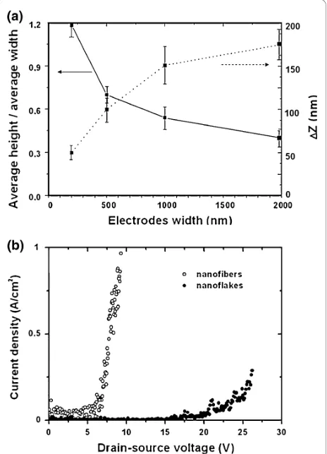
A systematic investigation of the morphology of the organic nanostructures was made for different electrode widths w, by measuring the dimensions (width and height) of the grown nanostructures by SEM and AFM, respectively, and by calculating the aspect ratio, i.e. height-to-width ratio, as well as the difference between the maximum and minimum heights (ΔZ=Zmax- Zmin)
[image:3.595.57.290.88.254.2]along the long axis of each individual structure. Figure 3a shows how these factors change as a function of the electrode width w. The data are based on mea-surements on about 120 nanostructures. For wide elec-trodes, the ratio between the average height and the average width of the nanostructures is smaller than for structures grown on narrow electrodes. We propose the following explanation for the phenomenon: on wide electrodes, the surface diffusion area is large, and p-6P clusters can aggregate and form long and flat fibers. On narrow electrodes, the surface diffusion area, where clusters are formed, is smaller, and the growth is
hindered by boundaries. As a consequence, the molecules grow preferentially side by side in the vertical direction since tail-to-tail growth for rod-like molecules is improbable. The structures grown on wide electrodes exhibit a more jagged morphology, as previously shown forp-6P nanofibers grown on gold surfaces [21,22]. This effect is also shown in Figure 3a, which shows an increase inΔZfor structures grown on wider electrodes. Figure 3b shows electrical measurements made by applying a voltage between the drain–source electrodes and measuring the current flowing through the organic nanofibers/flakes grown on narrow (w = 200 nm) and wide (w= 2μm) electrodes, respectively, with zero volts applied to the gate. Measurements prior top-6P deposi-tion were performed to verify that the measured current is not related to any leakage current. The current den-sity values were calculated by dividing the measured current with the total nanofiber/nanoflake cross-sectional area. The curves confirm that it is possible to
Figure 2a, b AFM images of gold electrodes withg= 200 nm and aw= 150 nm (nanoflakes) and b 2.4μm (nanofibers) after
[image:3.595.307.539.330.652.2]p-6P deposition. The cross-sectional profiles of both organic structures are shown in (c).
establish direct electrical connection to organic nano-structures and shown here is a clear difference in the electrical characteristics for the different structures with significantly higher current densities in the nanofibers even at relatively low voltages.
In order for a field-effect transistor to reach satura-tion, short-channel effects should be avoided by having a channel length that is at least 10 times larger than the gate oxide thickness [25,26]. All experiments presented here have been made on substrates with 100 nm oxide, so in order to minimize short-channel effects, the chan-nel length i.e. the gap to be bridged should be increased to 1 μm. The first experiments on platforms with gaps of these dimensions showed that the nanoflakes or nanofibers are not able to bridge such long gaps. In order to determine the maximum gap that the organic structures can bridge, a set of devices with var-ied electrodes widths w and separation gaps g were fabricated and investigated. Figure 4 illustrates the prob-abilities for the organic nanostructures to bridge at different configurations. The data were extracted from around 150 devices, and it shows the probability for the device to have at least one bridging structure. Forg < 200 nm, the probability for bridging structures is 1, but it decreases when gincreases, and it is 0 for g= 1 μm. Therefore, the chosen standard separation gap was 200 nm.
It should be noted that growth parameters such as the substrate temperature during deposition and the nom-inalp-6P thickness have a large influence on the prob-ability for the nanostructures to bridge the gaps. In the
present experiments, the substrate temperature was kept constant at 185°C and the nominal thickness was 20 nm. It was observed that there was a high probability for the nanostructures to bridge the gaps under these conditions. At even higher surface temperatures, no nanostructure growth was observed.
More elaborate results of the electrical characterization are shown in Figure 5a, which include output characteris-tics (IDSvs.VDS) for narrow (w= 200 nm) and wide (w=
2μm) electrodes. These were measured by sweeping the drain–source voltage from 0 V to positive voltages, back to negative voltages, and returning and finishing the mea-surement at 0 V. Each sweep was performed with a con-stant gate voltage (0 or -10 V). The conductivity of the nanostructures increases when a negative voltage is applied to the gate electrode, showing that the nanofibres or nanoflakes are p-type semiconductors. It is seen from Figure 5a that a lowerVDSis needed to conduct a current
[image:4.595.305.540.347.684.2]in the nanostructures grown on the wide electrodes (nano-fibers) compared to the structures grown on the narrow
Figure 4Probability for having at least one bridgingp-6P structure on a device with varied electrode widths and separation gaps.
[image:4.595.56.292.481.689.2]electrodes (nanoflakes), as was also seen in Figure 3b. We explain this difference in turn-on voltage by the fact that the nanofibers have a larger contact area to the gold elec-trode surface compared to the nanoflakes and therefore have a smaller contact resistance. We have not observed any saturation behavior even when the drain–source vol-tage is swept up to 70 V (at this volvol-tage, the fibers and flakes are destroyed); however, this is as expected since the electrode gap width to oxide thickness ratio is too small. Therefore, the field-effect mobility and the threshold vol-tage cannot be extracted from the data. The curves sweep-ing back to 0 V (Figure 5) show hysteresis. This effect is often observed for organic semiconductors [27] and is most likely due to charge trapping.
The transfer (IDSvs. VDS) curves for the devices
con-taining nanoflakes are shown in Figure 5b. The sweeps were made by sweeping the gate voltage from 0 to 20 V, back to -20 V, returning to 0 V. The drain–source vol-tage was kept constant at 0 and -20 V, respectively. These curves confirm that the nanoflakes behave as p-type semiconductors and exhibit an onset voltage of around -10 V.
Conclusions and Outlook
A method for growing in situ organic nanoflakes or nanofibers on a transistor platform was demonstrated in this work. The results show that the morphology of the nanostructures is strongly influenced by the drain and source electrodes width. When the gold electrodes are narrow, thep-6P molecules form high and narrow flake-like structures. This could be explained by topographical boundaries forp-6P diffusion on these substrates, which leads to more vertical aggregation. On wider gold electro-des, the larger surface diffusion areas lead to nanofiber growth, similar to growth on plane gold surfaces [21] (faceted morphology). The nanofibers start to conduct electrical current at lowerVDSthan the nanoflakes. The
proposed explanation for this behavior is that thep-6P nanofibers have a bigger contact area with the electrodes, which reduces the contact resistance. Both kinds of struc-tures present typical electrical characteristics of an organic semiconductor connected to a metal electrode in which a current starts to flow after application of a certain voltage.
Investigations of the maximum bridgeable gap were performed and showed a probability of 1 for nanostruc-tures bridging a gap of 200 nm. Since our oxide thick-ness is limited to 100 nm, the ratio between gap and insulator thickness is not high enough for the nanostructure transistor to reach saturation. However, electrical measurements show that an applied negative gate voltage increases the conductivity and thereby confirms that holes are the primary charge carriers.
The ability to pattern in situ growth of organic nano-fibers and nanoflakes on device platforms opens up a
route for use in a wide range of applications, such as large-scale fabrication of OLEDs and OFETs. We have demonstrated how the electrical properties of these structures can be altered by changing the structures morphology. In addition, nanofibers can be relatively straightforward assembled from other organic molecules with different optoelectronic properties [28]. For better transistor performance, one possibility would be to employ a bottom-contact/top-gate geometry that increases the contact area from which carriers inject.
Acknowledgements
This work was financially supported by the Danish Council for Technology and Innovation through the Octopus innovation consortium.
Received: 8 July 2010 Accepted: 12 August 2010 Published: 25 August 2010
References
1. Monat C, Domachuk P, Eggleton BJ:Nat Photonics2007,1:106-114. 2. Agarwal R, Lieber CM:Appl Phys A: Mater Sci Process2006,85:209-215. 3. Boukai AI, Bunimovich Y, Tahir-Kheli J, Yu J-K, Goddard III WA, Heath JR:
Nature2008,451:168-171.
4. Moran-Mirabal J,et al:Nano Lett2007,7(2):458-463. 5. Zaumseil J, Friend J, Sirringhaus H:Nat Mater2006,5:69. 6. Minot ED,et al:Nano Lett2007,7(2):367-371.
7. Duan X, Huang Y, Agarwal R, Lieber CM:Nature2003,421:241-245. 8. Law JBK, Thong JTL:Appl Phys Lett2006,88:133114.
9. Fan Z,et al:Nano Lett2008,8(1):20-25.
10. Svensson CPT,et al:Nanotechnology2008,19:305201.
11. Müllen K, Scherf U:Organic Ligth Emitting Devices.Wiley-VCH Weinheim, London; 2005.
12. Hoppe H, Sariciftci NS:J Mater Res2004,19:1924-1945.
13. Lim SJ, An BK, Jung SD, Chung MA, Park SY:Angew Chem Int Ed2004,
43:6346-6350.
14. Zheng KB, Shen HT, Ye CN, Li JL, Sun DL, Chen GR:Nano-Micro Lett2009,
1:23-26.
15. Ryu J, Kim S-W, Kang K, Park CB:ACS Nano2010,4:159-164. 16. Balzer F, Rubahn H-G:Appl Phys Lett2001,79:3860-3862. 17. Balzer F, Rubahn H-G:Nano Lett2002,2:747.
18. Balzer F, Rubahn H-G:Adv Func Mat2005,15:17.
19. Balzer F, Bordo VG, Simonsen AC, Rubahn H-G:Phys Rev B: Condens Mat
2003,67:115408.
20. Quochi F, Cordella F, Mura A, Bongiovanni G, Balzer F, Rubahn H-G:J Phys Chem B2005,109:21690.
21. Balzer F, Kankate L, Niehus H, Frese R, Maibohm C, Rubahn H-G:
Nanotechnology2006,17:984-991.
22. Madsen M, Kjelstrup-Hansen J, Rubahn H-G:Nanotechnology2009,
20:115601/1-5.
23. de RM, Hansen O, Kjelstrup-Hansen J, Rubahn HG:Nanoscale2010,
2:134-138.
24. Madsen M, Kartopu G, Andersen NL, Es-Souni M, Rubahn H-G:Appl Phys A
2009,96:591-594.
25. Chua LL, Ho PKH, Sirringhaus H, Friend RH:Appl Phys Lett2004,84:3400. 26. Frank DJ, Dennard RH, Nowak E, Solomon PM, Taur Y, Wong HSP:Proc IEEE
2001,89:259.
27. Jung T, Dodabalapur A, Wenz R, Mahapatra S:Appl Phys Lett2005,
87:182109.
28. Schiek M, Balzer F, Al-Shamery K, Brewer JR, Lützen A, Rubahn H-G:Small
2008,4:176.
doi:10.1007/s11671-010-9758-z
Cite this article as:Hansenet al.:In situ–Directed Growth of Organic Nanofibers and Nanoflakes: Electrical and Morphological Properties.