N A N O E X P R E S S
Open Access
Characterization of Films with Thickness Less
than 10 nm by Sensitivity-Enhanced Atomic
Force Acoustic Microscopy
Mikio Muraoka
*, Shinji Komatsu
Abstract
We present a method for characterizing ultrathin films using sensitivity-enhanced atomic force acoustic
microscopy, where a concentrated-mass cantilever having a flat tip was used as a sensitive oscillator. Evaluation was aimed at 6-nm-thick and 10-nm-thick diamond-like carbon (DLC) films deposited, using different methods, on a hard disk for the effective Young’s modulus defined as E/(1 -ν2), whereEis the Young’s modulus, andνis the Poisson’s ratio. The resonant frequency of the cantilever was affected not only by the film’s elasticity but also by the substrate even at an indentation depth of about 0.6 nm. The substrate effect was removed by employing a theoretical formula on the indentation of a layered half-space, together with a hard disk without DLC coating. The moduli of the 6-nm-thick and 10-nm-thick DLC films were 392 and 345 GPa, respectively. The error analysis showed the standard deviation less than 5% in the moduli.
Introduction
The protective coating for hard disks, namely a dia-mond-like carbon (DLC) film, is now targeted for thick-ness less than 3 nm because of the reduced spacing between the magnetic layer and the read/write head [1]. The mechanical properties become very important for reliability of the devices. The chemical structure of DLC significantly depends on the deposition process and influences the mechanical properties such as elasticity and hardness. Especially the Young’s modulusE drasti-cally varies with a content of sp3-bonds, which form three-dimensional interlinks in the amorphous network of carbons (E ≈ 100–800 GPa) [2-4]. Therefore, the modulus is useful to identify the chemical structure of films.
Various approaches for the determination of the elas-tic properties of thin films have been previously used, including nanoindentation [5], laser spectroscopic meth-ods [3], and removed substrate methmeth-ods [4]. However, it is still a challenging problem to evaluate ultrathin films like DLC films with thickness less than 10 nm.
Atomic force acoustic microscopy (AFAM) [6] is a promising method, which belongs to a family of dynamic techniques of atomic force microscope (AFM) such as micro-deformation microscopy [7] and ultraso-nic atomic force microscopy [8]. AFAM measures the resonant frequencyfof an AFM cantilever whose sensor tip is in contact with a sample oscillated by a piezoelec-tric device. If an appropriate order of the vibration mode is selected, fvaries with the contact stiffness k*, namely the interactive force gradient between a tip and a sample. The effective Young’s modulus Es* of a sam-ple, defined as Es / (1−s2) (Es: the Young’s modulus, νs: the Poisson’s ratio), is evaluated using contact mechanics relatingk* to Es*.
Characterization of a 50-nm-thick Ni film deposited on a Si substrate was demonstrated in AFAM, where f was observed without the substrate effects [9]. In regard to DLC thin films, only relative evaluation was per-formed [10]. These studies required a blunt tip with a radius of about 200 nm and a stiff cantilever of spring constantkc≈ 50 N/m to realize reproducible measure-ments. However, the requirement reduced the spatial resolution and the sensitivity in detection of the contact force.
When attempting to analyze difficult samples like a DLC film with thickness less than 10 nm, higher * Correspondence: [email protected]
Department of Mechanical Engineering, Akita University, 1-1 Tegatagakuen-machi, Akita, 010-8502, Japan.
performance of AFAM is required on the detection ofk* and the spatial resolution. We previously proposed a concentrated-mass (CM) cantilever as a way of enhan-cing the sensitivity in k*-detection without trade-offs [11]. A CM cantilever assures the maximum sensitivity for any sample material. Also, a flat tip with ductile-metal coating, keeps a stable contact area of a radius less than 5 nm and drastically simplifies the relation betweenk* and Es* [12].
The method we previously developed, termed sensitiv-ity-enhanced AFAM [12], is extended in this letter to the determination of the elastic modulus of ultrathin films. The demonstration was carried out for DLC films with thickness of 6 and 10 nm, deposited on a hard disk. A curve relating f to Es* was determined from multiple measurements on reference samples. The uncertainty was discussed by error analysis. In the eva-luation of the DLC-coated samples, the substrate effect was taken into account by using an analytical model for indentation of a layered half-space [13].
Experimental Procedure and Theory
CM Cantilever and Apparatus
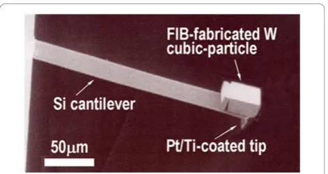
The experimental procedure is described elsewhere in detail [11,12]. We will briefly explain it here. The main body of a CM cantilever was a rectangular cantilever made of single-crystalline silicon (μMasch Co. Ltd.,kc= 0.65 N/m, fundamental resonant frequency 40.9 kHz). The silicon tip had an apex radius of about 10 nm and was coated with a 25-nm-thick Pt/Ti film. The coated tip was plastically deformed on a flat diamond surface under a contact load of 2 μN to give it a flat-ended shape. This plastic deformation also induced a work-hardening of the coating, which would prolong the life-time of the coated tip [12]. For the concentrated mass, a tungsten (W) particle of 35 × 33 × 20 μm in size was micro-machined from a W sheet of 20 μm thick by focused ion beam (FIB). The particle’s mass was about 445 ng, which corresponds to a mass ratio of 10.9, namely the ratio of the particle’s mass to the silicon-cantilever’s mass. The particle was attached adhesively to the free end of the cantilever by micromanipulation. Figure 1 shows a scanning electron micrograph of the CM cantilever. The main difference from the previous works [11,12] was in the use of the micro-machined particle instead of a deoxidized random particle for the concentrated mass. Another difference was in the pro-cess that a flat tip was formed from a virgin tip, not from a tip wasted after several tens of scans for imaging. An atomic force microscope (SII Co. Ltd., SPI3700-SPA270) was used in so-called contact mode for obser-ving the contact resonance spectra. The amplitude of cantilever vibration was acquired with a lock-in amplifier through a heterodyne down-converter.
A piezoelectric device placed beneath a sample was used for the oscillation. The time-averaged cantilever deflec-tion signal, which corresponds to the contact forceFe, was maintained through a built-in feedback circuit, where the electronic circuit is not subjected to sinusoi-dal signals at ultrasonic frequencies. The resonant frequency was measured at five to ten different locations on a sample to confirm reproducibility. All experiments were carried out at a temperature of 20–25°C and rela-tive humidity of about 40–50%.
Reference and DLC Samples
The reference samples and the elastic moduli are listed in Table 1. We employed a sapphire (0001) wafer in addition to silicon wafers and a diamond (100) used in the previous work [12]. These values were deduced from the crystal moduli determined by ultrasonic velo-city techniques for bulk samples (see appendix for sapphire).
DLC films of 6 nm thick and 10 nm thick were depos-ited on a substrate by sputtering a carbon target in Ar gas and by plasma-assisted chemical vapor deposition (CVD), respectively. The film thickness was estimated based on the deposition time. The substrate was a hard disk, which consisted of metallic multi-layers for mag-netic record and a glass substrate, namely (50-nm-thick Co-Cr-alloy layer)/(70-nm-thick Ti-alloy layer)/(0.6-mm-thick glass substrate). Also, the substrate without DLC coating was tested for the elastic modulus.
Theory for Evaluation of Thin Films
The resonant frequency (f) of a CM cantilever increases with the contact stiffness (k*) in accordance with the spring-mass model, namely k*/kc = (f/f0)2, wheref0 is the fundamental resonant frequency in the absence of a sample. A flat tip maintains a constant contact area independent of the adhesion force and the contact force. This also ensures constant k*. The theoretical formula
[image:2.595.305.541.87.212.2]k* = 2aE* for a flat-ended punch [14] is applicable,
whereais the radius of the contact area.E* is the effec-tive Young’s modulus of the contact region, defined as 1/E∗ =1/E*t +1/Es*. E*t[=Et / (1−t2)] is the effective Young’s modulus of a tip. These equations give the formula relatingfto E*s [12]:
f AE E
E E
= + 2 t s
t s * *
* *, (1)
where A(=a f02/kc) is a factor proportional to the contact radius. Both E*t andAcan be determined from thefmeasurements for reference samples.
Analytical models on indentation of a layered half-space for a circular punch proved the validity of the fol-lowing empirical formula [13]:
1 1
1 1
E E
t
a E
t a
s film sub
* = * −exp − * exp ,
⎛ ⎝⎜
⎞ ⎠⎟ ⎡
⎣
⎢ ⎤
⎦
⎥ + ⎛⎝⎜− ⎞⎠⎟
(2)
where Efilm* and E*sub are the effective Young’s
mod-uli of a film and a substrate, respectively. The coefficient gis a function ofa/t, wheretis the film thickness. The numerical result on a relation of ganda/twas graphi-cally shown in reference [13]. Note that the symbolain reference [13] is defined as the square root of the con-tact area, which differs from the definition of a (the radius of the contact area) in this letter, and theng mul-tiplied by π1/2 equals the symbol a in reference [13]. Examples of the numerical result are indicated with cir-cles in Figure 2. The numerical data can be well fitted by the following formula.
=
(
)
+ +
c a t
a t c a t c
n
n n
0
0
1
2 2 3
/
( / ) ( / ) , (3)
where c0 = 0.4684, c2 = 0.009968, c3 = 1.004, n0 = 0.4910,n1 = 1.736, and n2 = 6.607 are the coefficients determined by a nonlinear least-square fit.
Errors in E*s for a sample come from uncertainties
in the predetermination of A and Et* and in the f measurement for the sample, which are represented by the standard deviations sA, sE t, and sf, respectively. The standard deviation sEs of Es* can be estimated by the error propagation on Eq. 1: Es2 =D2AA2 −2D DA Et A Et+DEt2Et2 +Df2f2,
where DA = ∂E*s/∂A D, Et = ∂E*s/∂E*t and Df= ∂E*s/∂f. In term of the covariance between Aand Et*, the correla-tion coefficient is set to -1, the validity of which was confirmed in the fitting of Eq. 1. Assuming negligible errors in g and a/t, the standard deviation sEfilm of E*film is estimated by the error propagation
on Eq. 2: Efilm2 = Es2Es2 + Esub2 Esub2
D D , where
DEsub= ∂Efilm* /∂Esub* , DEsub = ∂E*film/∂E*sub, and sEsub is the standard deviation of Esub* .
Results and Discussion
Effective Young’s Modulus of a Flat Tip and the Contact Radius
The CM cantilever in free space measuredf0= 9.917 kHz for the fundamental resonant frequency. Figure 3 shows spectra for the reference, Si (100) wafer. The resonant frequency seems to become independent of the contact force (Fe) when increasingFe. This reflects the constant contact area observed in the case of the flat tip.
[image:3.595.57.540.102.164.2]To measuref, we setFeto be a value as small as possi-ble, at which the resonant peak was clear and settled in frequency. The value depended on the sample material. The resonance frequencies for Si (100), Si (111), Al2O3 (0001), and diamond (100) were f= 199.3 ± 1.3 kHz, 218.6 ± 1.9 kHz, 254.5 ± 1.1 kHz, and 281.0 ± 1.1 kHz, whereFeis set to 300, 400, 500, and 700 nN, respectively. The errors show the 95% confidence regions (±2s). The excellent reproducibility was attained in the
Table 1 Elastic moduli of reference samples
Reference sample Young’s modulusEs(GPa) Poisson’s ratio (νs) Effective Young’s modulus Es*=Es/ (1−s2) [GPa]
Diamond (100) 1050 0.1 1061
Sapphire (0001) 451.2 0.172 465.1
Silicon (111) 187.9 0.180 194.2
[image:3.595.304.540.532.673.2]Silicon (100) 130.0 0.278 140.9
measurements for 5–10 different positions on each refer-ence surface. Figure 4 shows examples of spectra for the reference samples.
Fitting Eq. 1 to the relationship between the resonant frequencies measured for reference and the effective Young’s moduli listed in Table 1, we determined
A(=a f02/kc) and Et*, which are hard to measure or
estimate directly. Figure 5 shows the least-squares fit obtained for the reference samples, which yielded A= 0.2496 ± 0.0061 (± 2s) m/kg and E*t = 184.6 ± 8.8
(± 2s) GPa. The errors forAand Et* correlate, and the
error’s sign is taken opposite to each other.
Use of the values of A,kc, andf0 produced a reason-able contact radiusa= 1.7 nm. Also, the value of E*t is comparable to the averaged value for bulk platinum (196 GPa) and bulk titanium (129 GPa), but close to the value for platinum differently from the previous work (Et* = 152.3 GPa) [12]. This would be on account of the contact area smaller than that in the previous work
(a = 4.4 nm) [12]. In the contact deformation of the present tip, the contribution of surface layer (Pt) would dominate rather than the insert layer (Ti).
The square of the correlation coefficient (r2 = 0.9987) of the fit confirms the validity of the theory on a CM cantilever with a flat tip. The error bar for each data point and the broken curves in Figure 5 indicate the 95% confidence regions.
Evaluation of DLC Thin Films
The samples coated with the 6-nm-thick DLC film (Sputter) and the 10-nm-thick DLC film (CVD) mea-sured f = 240.4 ± 1.6 (± 2s) kHz and f = 239.6 ± 0.5 (± 2s) kHz, where Feis set to 600 and 800 nN, respec-tively. The DLC coating shifted the resonant frequency to higher than that of the sample without DLC coating [f = 229.8 ± 1.6 (± 2s) kHz (Fe= 500 nN)]. Also, the values offfor the two DLC films were alike despite the different thickness. This does not mean that the reso-nance is free from the substrate effects.
The effective Young’s modulus of a sample was determined from the curve in Figure 5 to be Es* =
310.5 ± 11.4 GPa, 305.2 ± 3.5 GPa, and 247.8 ± 8.2 GPa for the hard disks with 6-nm-thick DLC (Sputter), 10-nm-thick DLC (CVD), and without DLC coating, respectively. The errors are in the 95% confidence regions. The last one corresponds to Esub* . The value of Esub* was similar to the modulus of Co-Cr alloys (230–280 GPa) [15,16].
Substituting the values of Esub* and Es* into Eq. 2, we obtained the effective Young’s modulus of a film (Efilm* ), where g was calculated using a= 1.7 nm and
[image:4.595.55.291.88.245.2]t= 6 nm or 10 nm. The moduli were Efilm* = 391.8 ± 34.7 (± 2s) GPa and 345.1 ± 8.5 (± 2s) GPa for the 6-nm DLC (Sputter) and the 10-nm DLC (CVD),
[image:4.595.303.539.523.655.2]Figure 3The spectra of the CM cantilever vibration in contact with silicon (100) when increasing the contact force (Fe).
Figure 4The spectra for reference samples [Si (100), Si (111), Al2O3(0001), and diamond (100)] and hard disk samples [6
nm-DLC (Sputter), 10 nm-DLC (CVD) and Co-Cr alloy (hard disk without DLC)].
[image:4.595.57.293.541.669.2]respectively. The presence of substrate effects was clear in that the values of Es* for the 6-nm-film-coated and 10-nm-film-6-nm-film-coated samples were 20 and 10% less than the corresponding values of Efilm* , respectively. The values of E*film were within the range of values reported for several DLC films, from 100 to 800 GPa [2-4]. Also, a good precision of 2s < 10% was attained.
An error in a/t, which was neglected in the present evaluation, also causes uncertainty of the results. A pos-tulated error of 20% in a/t results in a relatively small error of about 5 and 2.5% in Efilm* for the DLC films of 6 nm thick (a/t= 0.283) and 10 nm thick (a/t= 0.17), respectively. The resulting error increases with a/t. Therefore, the contact radius (a) should be minimized.
The indentation depth δs, namely the total displace-mentδ(=Fe/k*) minus the tip deformation, can be esti-mated by taking account of the contribution of a sample, ks*=2aE*s, in the contact stiffness. The estimate was s =Fe/k*s = 0.57 nm and 0.77 nm for the 6-nm-DLC and 10-nm-6-nm-DLC samples, respectively. These indentation depths are 10% or less of the film thickness. The substrate effect should be carefully considered even when AFAM is applied. The present method provides the AFAM method of determining the elastic modulus for ultrathin films, eliminating the influence of a sub-strate. The sensitivity-enhanced AFAM proved to be sensitive enough for the determination of the ultrathin film elasticity and to have the excellent repeatability and reliability.
Conclusion
The 6-nm-thick and 10-nm-thick diamond-like carbon (DLC) films on a hard disk were evaluated for the effective Young’s modulus using sensitivity-enhanced atomic force acoustic microscopy. The modulus was determined from the measurements of the contact resonant frequency with the aid of a theory on inden-tation of a layered half-space. The moduli of the 6-nm DLC and 10-nm DLC were 391.8 ± 34.7 GPa and 345.1 ± 8.5 GPa, respectively, which reflected differ-ence in the method of film deposition. The errors, the 95% confidence regions (± 2s), show that this method gives a precise estimate of the effective Young’s modulus.
Appendix
Calculations of the modulus are alike for cubic crystals like diamond and silicon [12] and for trigonal crystals like sapphire (Al2O3). A trigonal crystal, however, has
more constants, c11, c12, c13, c14, c33, and c44, than a cubic crystal. They relate stressessito strainsεi(i= 1 - 6) as follows:
1 11 1 12 2 13 3 14 4
2 12 1 11 2 13 3 14 4
3 13
= + + +
= + + −
=
c c c c
c c c c
c (( )
( ) (
1 2 33 3
4 14 1 2 44 4
5 44 5 14 6
6 14 5
+ + = − + = − = − + c c c c c
c cc11−c12)6/2
(4)
where the subscripts adopt an abbreviated notation (e.g., s1 = s11, and s4 = s23) [17]. All components are referred to Cartesian coordinates xi (i = 1 - 3), where the x1 and x3 axes are taken along the a1-axis [1000] and the c-axis [0001], respectively. Calculation of the effective Young’s modulus for the C-plane (0001) requires the Young’s modulus E[0001] in the direction of the c-axis. Eliminating ε1, ε3, and ε4 in Eq. 4 under the condition of uniaxial stressingsi = 0 (i ≠ 3), we can obtain the following formula from
E[0001]=s3/ε3.
E c c
c c
[0001] 33 13 . 2
11 12 2
= −
+ (5)
While the Poisson’s ratioν[0001]depends on the direc-tion in which lateral strain is measured, we let ε1 (= ε2) represent lateral strain for simplicity. This simplifies the calculation ofν[0001]:
[0001] 1 .
3 2 3 13 11 12 ≈ − = − = + c
c c (6)
The elastic moduli for sapphire in Table 1 were obtained from Eqs. 5 and 6 together with the single-crystal constants, c11 = 490.2 GPa, c12 = 165.4 GPa,
c13= 113.0 GPa, andc33= 490.2 GPa [18].
Acknowledgements
We extend our appreciation to Mr. Fukunori Izumida of Iwate Industrial Research Institute and Mr. Shunsuke Goto of LIGHTOM, Inc., for their assistance in micro-machining the concentrated mass, to Dr. Jun Ariake of Akita Institute of Advanced Technology for providing the DLC-coated hard disk samples, and to Mr. Yasuyuki Hasebe of MAHK Co., Ltd., for his generosity in proffering the sapphire wafer. This work was supported by the Japan Society for the Promotion of Science under a Grant-in-Aid for Science Research (S) 18106003, (A) 20246028, and (B) 20360049.
References
1. Cord B, Scherer J:IEEE Trans Mag2000,36:67.
2. Schultrich B, Scheibe HJ, Dresher D, Ziegle H:Surf Coat Technol1998, 98:1097.
3. Ferrari AC, Robertson J, Beghi MG, Bottani CE, Ferulano R, Pastorelli R:Appl Phys Lett1999,75:1893.
4. Chung J-W, Lee C-S, Ko D-H, Han JH, Eun KY, Lee K-R:Diam Rel Mater2001, 10:2069.
5. Pharr GM, Callahan DL, McAdams SD, Tsui TY, Anders S, Anders A, Ager JW, Brown IG, Bhatia CS, Silva SRP, Robertson J:Appl Phys Lett1996,68:779. 6. Rabe U, Janser K, Arnold W:Rev Sci Instrum1996,67:3281.
7. Cretin B, Sthal F:Appl Phys Lett1993,62:829. 8. Yamanaka K, Nakano S:Jpn J Appl Phys1996,35:3787.
9. Kopycinska-Müller M, Geiss RH, Müller J, Hurley DC:Nanotechnology2005, 16:703.
10. Amelio S, Goldade AV, Rabe U, Scherer V, Bhushan B, Arnold W:Thin Solid Films2001,392:75.
11. Muraoka M:JSME Int J A2002,45:567. 12. Muraoka M:Nanotechnology2005,16:542. 13. King RB:Int J Solids Struct1987,23:1657. 14. Sneddon IN:Int J Eng Sci1965,3:47.
15. Davidson JA, Mishra AK, Kavacs P, Poggie RA:Biomed Mater Eng1994,4:231. 16. Black J, Hastings GW:Handbook of Biomaterials Properties.Chapman and
Hall, London; 1998.
17. Thurston RN: InPhysical Acoustics I–Part A.Edited by: Mason WP. Academic, New York; 1964:.
18. Anderson OL: InPhysical Acoustics III–Part B.Edited by: Mason WP. Academic, New York; 1965:.
doi:10.1007/s11671-010-9778-8
Cite this article as:Muraoka and Komatsu:Characterization of Films with Thickness Less than 10 nm by Sensitivity-Enhanced Atomic
Force Acoustic Microscopy.Nanoscale Res Lett20116:33.
Submit your manuscript to a
journal and benefi t from:
7Convenient online submission
7Rigorous peer review
7Immediate publication on acceptance
7Open access: articles freely available online
7High visibility within the fi eld
7Retaining the copyright to your article
![Figure 2 Relationship betweenrepresents the numerical result obtained by the theoreticalanalysis for indentation of a layered half-space [13], and thesolid curve is a least-square fit of Eq](https://thumb-us.123doks.com/thumbv2/123dok_us/8847022.933456/3.595.304.540.532.673/figure-relationship-betweenrepresents-numerical-obtained-theoreticalanalysis-indentation-thesolid.webp)

