Energy Efficiency Enhancement for 45nm 1Mb SRAM
Array Structures
Mamatha Samson,
Ph.D.GNITS for women Hyderabad
Madhulatha
AMITECH PVT. LTD (INDIA) Hyderabad
ABSTRACT
Energy efficiency is a supreme design concern in many ultralow-power applications. In such applications, high density Static Random-Access Memory (SRAM) plays a significant role. This paper explores and analyzes 1Mb SRAM array structures for energy efficiency improvement by adopting circuit modifications and inclusion of charge sharing circuits. The analysis shows that the array structure optimization and charge accumulator circuits can improve the energy efficiency for the same SRAM bit density and the same supply voltage.
Keywords
Six-transistor (6T) Static Random-Access Memory (SRAM), energy efficiency, minimum energy, SRAM, charge-share
1.
INTRODUCTION
Extremely low power SRAM is required in many applications like wearable devices sensor nets and mobile applications. There are various approaches that are adopted to reduce power dissipation in SRAM arrays like power supply voltage scaling and power gating. Lower power supply voltage reduces the dynamic power in quadratic fashion and leakage power in exponential way. But results in reduced noise margin. Forward body biasing methods and multi Vt techniques are used to reduce sub threshold leakage current High dielectric constant gate technology decreases the gate leakage current. Energy loss is reduced by Adiabatic charging technique. The SRAM working purely on adiabatic charging principles need multiple phase power clocks [1]. Although there is huge saving in energy during writing as well as reading, the design of the SRAM circuit is complex and not same as the design of conventional SRAM. The latency of operation is more. In energy recovery approach, energy stored in the bit line capacitance that is normally lost to ground during writing is collected and pumped back into the source. Based on the phase of the charging source, pre charging techniques, sense amplifier, the complexity and area of the pumping circuit, there are variants [2, 3, 4 and 5]. The pumping circuit add to the area of the SRAM array.
To overcome the design complexity and latency of complete adiabatic SRAMS, SRAMs that make use of adiabatic charging technique partially have been designed. High resistivity switches are used to vary the power supply voltage slowly in [6].Based on whether adiabatic charging is applied to only power supply line or ground line or bit lines and word lines or only bit lines, there are many types of adiabatic SRAMs [7,8 9 and 10].
Energy stored in the bit lines is recycled by the help of switches to adjacent bit lines in order to save energy in bit line
charge- recycle method. This method reduces the swing voltages to a low swing voltage. Based on whether energy recycling is done only during writing cycle or during both writing and reading cycles, there are variants [11 and 12] The circuit uses power switches and complex switching mechanism.
This paper describes the implementation of circuit techniques [13] that effectively use the charge of the non-selected bit lines by charge sharing methods in case of structurally optimized 1Mb SRAM array and the results obtained are compared with the SRAM array without these techniques adopted.
2.
DESIGN DESCRIPTION
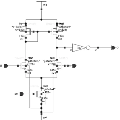
45nm 1 Mb 6T SRAM array with row and column decoders, bit-line conditioning circuitry, read-write control circuitry, sense amplifiers and clock tree buffers is implemented using hierarchical bit line architecture[Fig.1] in cadence environment. A SRAM cell [ Fig.2] is first tested for its working.
Hierarchical bit lines limit the excess bit line swing. The sense amplifiers [Fig.3] in the short local bit lines (LBL) become inactive after the word line falls. The charges from the selected local bit lines pass to the global bit lines by charge sharing method. During writing the charge is pumped back to the global bit lines with the help of write driver circuit as shown in the Fig. 4.
16COLUMNS 2 0 4 8 R O W S
X16
4
X3WL
Selected column LB L G B L Sense AmplifierL L L
L
Figure 2: 6t SRAM Cell
The charge (electrons) in the local bit lines which are not selected are allowed to pass to global bit lines (GBL) with the help of switches. Hence the wasted power consumption caused by excess swing of the bit lines is also suppressed. The global bit lines get charges and can support many local lines. The sense amplifiers implemented is differential amplifier type. It is shown in the Fig. 3. The nand type of row decoder addresses the word lines.
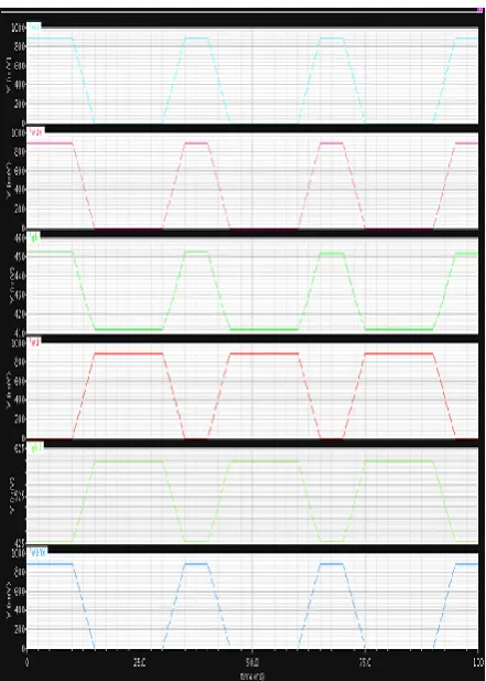
[image:2.595.324.536.74.597.2]The performance of the SRAM cell under noisy conditions is evaluated with the help of SNM [14]. It is found to be 0.34V. The corresponding butterfly curve is plotted as shown in the Fig. 6. The wave forms of the one of the SRAM cells during writing is shown in the Fig. 7 and for a cell in an array of size 1 MB is shown the Fig. 8. The waveforms corresponding to Charge collector circuit is shown in the Fig. 9.The waveforms corresponding to charge sharing circuit is shown in the Fig. 10.
The leakage power of a 6T SRAM cell with power supply voltage equal to 1V is 924.5E-6 watts. The power comparison is carried with the similar SRAM array without energy saving from non selected bit lines. The readings are tabulated in the Table 1.
[image:2.595.326.540.79.288.2]Figure 3 Sense amplifier
Figure 4 Write Driver circuit (WDC).
Figure 5 Charge Collector Circuit (CCC).
Figure 6 Write operation of a single 6T SRAM cell. Global
bit line
Global bit line
Write enable
[image:2.595.327.527.306.582.2] [image:2.595.68.272.523.727.2] [image:2.595.333.526.613.750.2]Figure 7 Write and read operation of the 6T SRAM cell in an array of size 1Mb
Figure 8: Read static noise margin
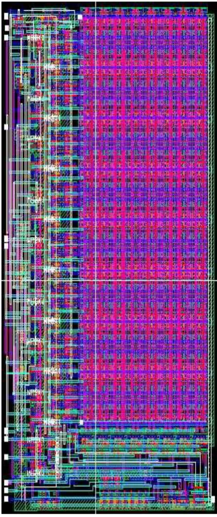
The leakage power of a 6T SRAM cell with power supply voltage equal to 1V is 924.5E-6 watts. The power comparison is carried with the similar SRAM array without energy saving technique from non selected bit lines. The readings are tabulated in the Table 1. The power saving is found to be 1Mb 47.7%. at 1V power supply voltage and 63% at 0.58V power supply voltage. The difference is due to reduced dynamic power consumption.The schematic of the entire 1 Mb SRAM Array is shown in the Fig. 12 and the corresponding layout is shown in the Fig. 13 respectively.
[image:3.595.322.537.70.424.2]The various 6T SRAM cell parameters (per SRAM cell) are found out. Diffusion capacitance of access transistors is 1.0512fF. Word line capacitance is 0.076fF. Gate capacitance of access transistors is 1.4832fF. The cell area is 29.33 µm2 .
[image:3.595.66.268.237.414.2]Table 1: Power comparisons of SRAM array with and without charge collection.
Fig. 9 Wave forms of Charge Collecting Circuit
Figure 10 Wave forms of Charge Sharing Write circuit S
No Circuit Name
Power Dissipation
(µw) at 0.7V
Power Dissipation
(µW) at 0.59V
1
SRAM array with Charge Collector Circuits.
209.3 μW 51.36 μW
2
SRAM array without Charge Collector Circuits.
[image:3.595.319.540.439.748.2]Figure 11 The schematic view of the SRAM array
3.
CONCLUSION
The schematic and the layout of 1Mb SRAM Array of have been drawn in Cadence environment using Virtuoso tool. The charge from the unused bit lines are successfully utilized during writing with the help of switching circuits. The power dissipation of the SRAM array with Charge Collector Circuits is compared with that of SRAM array without Charge Collector Circuits .The power saving is found to be 47.7%, when the power supply voltage is 1V. The low power SRAM array can find application in mobile devices and biomedical applications. This type of charge collection can be extended to
other memory circuits. Figure 12 Layout of the design
4.
REFERENCES
[1] D. Somasekhar, Yibin Ye, Kaushik Roy, “An Energy Recovery Static RAM Memory Core, In Proc. 1995 Symposium on Low Power Electronics”, San Jose, CA, October 9-1, 1995
[2] N. Tzartzanis and W.C. Athas, “Energy recovery for the design of high-speed, low power static RAMs,” In Proc. IEEE International Symposium on Low Power Electronics and Design pp. 55–60, 1996
[3] Joohee Kim, Conrad H. Ziesler, Marios C. Papaefthymiou “Energy Recovering Static Memory” In
Proc. ISLPED’02, Monterey, California, USA, August 12–14, 2002
[4] Joohee Kim,M.C Papaefthymiou, In Proc. “Constant – Load Energy Recovery Memory For Low Power, International Symposium on Low power Electronics and Design,pp.240-243. 2004
[image:4.595.316.539.81.612.2][6] Shunji Nakata in “Recent Patents on Electrical Engineering, 2009, Vol.2,No.1
[7] Byung-Do Yang “A Low Power SRAM Using Bit Line Charge –Recycling for Read and WriteOperations in IEEE Journal of Solid-State Circuits, Vol.45, No. 10, October 2010
[8] Jun-Jun Yu, Peng-Jun Wang “Design of Adiabatic SRAM Based on CTGAL Circuit”. In Proc. The 8thInternational Conference on Solid State and Integrated-Circuit Technology, October 23-26, 2006 [9] Hao-I Yang,Ssu-Yun Lai,and Wei Hwang “Low-Power
Floating Bit line 8-T SRAM Design with Write Assistant Circuits” In Proc. IEEE International SOC Conference ,October, 2008
[10]Shunji Nakata,Hirotsugu Suzuki,Ryota Honda,Takahito Kusumoto,Shinjchiro Mutoh, Hiroshi Makino, Masayuki Makino, Masayuki Miyama and Yoshio Matsuda “ Adiabatic SRAM with a shared Access Port using a Controlled Ground Line and Step-Voltage Circuit” In Proc. IEEE International Symposium on Circuits and Systems, ISCAS 2010, pp.2474-2477, 2010.
[11]Keejong Kim, Hamid Mahmoodi and Kaushik Roy “A Low Power SRAM Using Bit- Line Charge-Recycling” IEEE Journal of Solid State Circuits, vol.43, no.2, pp. 446-458, 2008
[12]Byung-Do Yang “A Low Power SRAM Using Bit Line Charge –Recycling for Read and Write Operations in IEEE Journal of Solid-State Circuits, Vol.45, No. 10, October 2010
[13]S. Moriwaki1, Y. Yamamoto1, A. Kawasumi1, T. Suzuki2, S. Miyano1, T. Sakurai3 and H. Shinohara1,”A 13.8pJ/Access/Mbit SRAM with Charge Collector circuits for Effective Use of Non Selected Bit Line Charges”. In Proc. Symposium on VLSI Circuits Digest of Technical Papers, 2012