Extending Systems-on-Chip to the Third Dimension:
Performance, Cost and Technological Tradeoffs
Roshan Weerasekera, Li-Rong Zheng
ECS/ICT/KTH,ELECTRUM 229, 164 40 Kista, Sweden. Email:{roshan,lirong}@kth.se
Dinesh Pamunuwa
Centre for Microsystems EngineeringLancaster University Lancaster LA1 4YR, UK. Email: [email protected]
Hannu Tenhunen
ECS/ICT/KTH, ELECTRUM 229, 164 40 Kista, Sweden. Email: [email protected]Abstract—Because of the today’s market demand for
high-performance, high-density portable hand-held applications, elec-tronic system design technology has shifted the focus from 2-D planar SoC single-chip solutions to different alternative options as tiled silicon and single-level embedded modules as well as 3-D integration. Among the various choices, finding an optimal solution for system implementation dealt usually with cost, performance and other technological trade-off analysis at the system conceptual level. It has been identified that the decisions made within the first 20% of the total design cycle time will ultimately result upto 80% of the final product cost.
In this paper, we discuss appropriate and realistic metric for performance and cost trade-off analysis both at system concep-tual level (up-front in the design phase) and at implementation phase for verification in the three-dimensional integration. In order to validate the methodology, two ubiquitous electronic systems are analyzed under various implementation schemes and discuss the pros and cons of each of them.
I. INTRODUCTION
As consumer demand for products that keep getting smaller, lighter and offer more functionality and performance for less power continues unabated, experimental electronic sys-tem implementation technologies are migrating towards 3-D solutions. A major driver behind this trend is the plethora of implementation problems facing gigascale 2-D integra-tion, ranging from technological to architectural. From a fabrication point of view, integrating disparate technologies such as sensors, MEMS structures, and other heterogeneous elements demanded by many applications on a single die is fraught with difficulties. The 2D architecture also results in numerous bottlenecks due to area and routing congestion, such as the memory bottleneck in multimedia SoCs [1]. Recent developments in fabrication technology have resulted in 3D integration being a potentially viable option for gigascale integration [2][3]. Major potential benefits of vertical inte-gration include increasing real estate by building upwards, and the reduction in the total length of wiring required for a given system configuration. The wire length reduction alone can reduce the interconnect energy and propagation delay by 51% and 54% respectively, at the 45 nm technology node [4]. The reduced parasitics for interconnects can significantly simplify the circuit and power distribution network design for high performance applications. In mixed-signal systems, Noise-sensitive analog/RF circuitry is prone to failure due to
interference from their digital counterpart through the base silicon substrate. 3-D integration aids in the solution for noise isolation since it separates the analog/RF and digital circuits into different substrates with the metal or the dielectric bonding layer used in wafer-bonding technology [5] providing an effective guard ring. The final footprint of the packaged system is also less for a 3-D implementation.
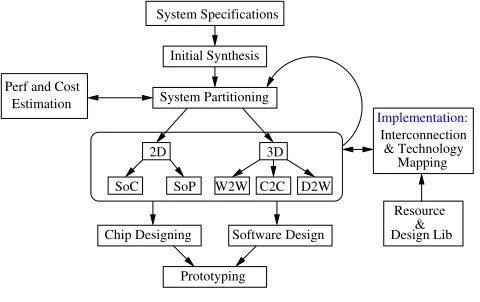
Estimation Perf and Cost
Initial Synthesis
System Partitioning
SoC W2W C2C
3D 2D
D2W
Prototyping
Chip Designing Software Design Design Lib System Specifications
Mapping Interconnection
SoP
& Technology
[image:1.612.316.556.321.472.2]Resource & Implementation:
Fig. 1. System Design Opportunities
The main obstacle to 3-D integration is poor thermal con-ductivity and heat dissipation and the resultant temperature rise due to the high power density [6]. A well known method to transfer heat outside is to use thermal vias, which further increases the routing congestion [7], [8]. However, careful thermal-via placement in high performance systems could effectively control the temperature in 3D-ICs. Some alternative methods proposed, such as integrated micro-channel cooling [9], [10] may also be a viable option. Moreover, it is shown in [11] that even though the increased temperature reduces the highest operating frequency, the overall system performance can still be comparatively better than in a 2-D implementation. However, even as designers are presented with an extra spatial dimension, the complexity of the layout and the ar-chitectural trade-offs also increase. To get a true improvement in performance, a very careful analysis using detailed models at different hierarchical levels is crucial. Even though several previous works have addressed this issue [12][13][14], they mostly concentrate on isolated model development, or target
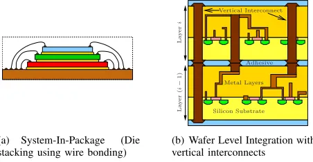
(a) System-In-Package (Die stacking using wire bonding)
Silicon Substrate Metal Layers Adhesive
La
y
e
r
(
i
−
1)
La
y
e
r
i
Vertical Interconnect
[image:2.612.64.290.61.178.2](b) Wafer Level Integration with vertical interconnects
Fig. 2. Three-Dimensional Integration options
some specific type of system. In this work, we present a cohesive analysis of the technological, cost and performance tradeoffs for digital and mixed-mode systems, outlining the choices available at different points in the design and their ramifications. To this end we collate existing models from the literature, and modify them and also derive new models as necessary, including an overall yield model, a cost model, performance metrics and a thermal profile model for both 2-D and 3-D integration technologies. The main contribution of this paper is in developing a generic methodology for performance and cost estimations of 3D systems that can be modified for different applications, and a comprehensive set of estimation models as building blocks. We also use this methodology to provide detailed estimates for two applications that showcase the potential benefits of 3D integration.
The rest of the paper is organized as follows; first, we discuss 3-D integration technologies, and go on to present our methodology for cost and performance estimation, including all models. In section IV we discuss the cost and performance issues for two different applications in detail. We end with a discussion and our conclusions.
II. THREE-DIMENSIONALINTEGRATION TECHNOLOGIES
To avoid confusion, we define a few terms at the outset to describe different packaging technologies. The term SoP is used to refer to a 2-D multi-chip module (MCM) arrangement where packaged chips are situated on a single substrate or across a board. A 3-D stacked arrangements of chips or dies is referred to as a System-In-Package or SiP. An electronic system that is laid out on a single chip in 2-D is referred to as a System-On-Chip or SoC. 3-D integration techniques can be basically categorized into two major schemes [15]: Folding and Stacking. In folding, a planar assembly with flexible substrate is folded into several layers in order to form a very compact shape. In this approach the interconnect length is longer than in the stacked approach described below, but a very compact size can be achieved.
Stacking chips or dies vertically is widely known as System-in-a-Package (SiP). Stacking can be done at the chip level with either chip-to-chip (C2C), Package-on-Package (PoP) or MCM-to-MCM bonding using epoxy or glues and creating electrical connections by wire-bonding techniques as illus-trated in figure 2(a). These techniques present the opportunity
to stack Known-Good-Dies (KGDs) in layers [16], improving the system yield. This approach has been using for hetero-geneous integration of mixed-signal systems, where different high-performance intellectual property (IP) blocks could also be integrated to achieve a better performance. As an alternative to chip stacking, 3-D integration can be performed at the wafer-level too. Different blocks can be processed on sepa-rate wafers, and they can be interconnected vertically using through-hole vias (THV) or through-Si vias (TSV) to form global communication links (refer figure 2(b)). This effectively reduce the latency and power drawbacks inherent to global communication in SoCs. Wafer-Level integration (WLI) can be performed in two ways; entire wafers can be bonded together before dicing (an approach herein after termed 3D-W2W) or KGDs are bonded on top of a host wafer containing other KGD sites termed (3D-D2W) [17]. Some other possibilities not considered here include capacitive [18][19] or inductive [20] links for wireless communication between chips [21].
In this analysis, we concentrate on stacking methodologies and compare between 3D-SiP, 3D-D2W and 3D-W2W tech-nologies.
III. PERFORMANCE ANDCOSTESTIMATIONMODELS
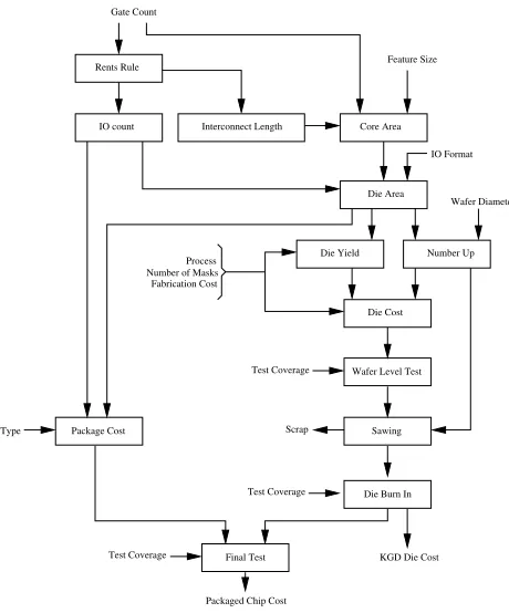
Previous works that addressed cost and performance trade-offs include [12] and [13], where Liu et. al. discuss the mapping from 2-D to 3-D under the constraints of perfor-mance, cost and temperature. However, they omit many 3-D technological details. The authors of [14] describe a yield and cost model for 3-D stacked chips with particular emphasis on how the yield is affected by the number of through-hold vias. We have previously illustrated how to make a design choice between SoC and SoP for mixed signal circuits [12]. The overall cost estimation process that we adopt is outlined in figure 3. The first task of the overall process is to find both chip/module area, because the cost and performance is predicted on the area. If not provided by the IP vendor the area of a digital module implemented in some target technology can be estimated in a straightforward manner, using gate information and technology scaling. However, the area of an analog chip depends not only on the number of transistors and their sizes (in practice, minimum size transistors are not used in analog circuits), but also the circuit architecture. For example, in a VCO, the area of the on-chip inductor may be hundreds of times larger than that of a transistor. In a ADC or DAC, on-chip resistors and capacitors also occupy a larger-fraction of total area. Full custom design experiences are necessary to estimate the size of an analog chip.
A. Die/SoP Area Models
The area occupied by the transistors and their interconnects is termed the core area (Acore) of the chip. This area can either
be Interconnect-Capacity limited or Transistor-Area limited. Given the number of total number of gates (Ng), and the gate
area (Ag), the core area is:
Acore=max
Ngd2g, NgAg
wheredgis the gate dimension andNp is the total number of
IO pads. The gate dimension is defined from [22] as
dg=
fgRmPw
ewnw
(2)
Here fg refers to the gate fanout, Pw to interconnection
pitch, nw to the number of interconnection layers, ew to the
utilization efficiency of interconnects, andRm to the average
interconnect length, which can be determined from Donath’s model [23]:
Rm= 2
9
1−4(p−1)
1−Ng(p−1)
7N(
p−0.5)
g −1
4(p−0.5)−1 −
1−Ng(p−1.5)
1−4(p−1.5)
(3) forp= 0.5, and
Rm= 2
9
1−4p−1 1−N gp−1
7log4N g− 1−N g
p−1.5
1−4p−1.5
(4)
forp=0.5.
When it comes to packaging the core, the number of I/Os to be connected to the outside must be arranged around the periphery and may require a larger perimeter than dictated by the core area in order to facilitate their placement according to the minimum peripheral pitch. Then, the die area is given by
Adie=max
(Acore+ 2Pp)2,
NpPp
4 + 2Pp
2 (5)
wherePp is the peripheral in-line pad pitch and Np is the
total number of IO pads.
Np is evaluated using the well-known Rent’s rule, the
empirical equation that estimates the growth in the number of signal pins on a circuit as a function of the logic components in it. It usually takes the form:
Np=K·Ngρ (6)
whereρis Rent’s exponent, K is Rent’s coefficient, andNg
is the number of logic gates on the chip or logic partition. Rents rule in this form is valid only for homogeneous systems, but not for more complex systems, where several different architectures are integrated to form an SoC. A form of Rent’s rule described in [24], which argues that the same power-law expression holds with an modifiedK andρparameters, given by:
Keq = Ng eq
n
i=1
KiNg i
(7)
ρeq =
n
i=1ρiNg i
Ng eq
whereKi andρi are the usual Rent’s rule parameters,Ngi is
the number of gates in block i, andNg eq =ni=1Ng i.
Multi-chip module (MCM) technology can be used as a possible implementation of SoP. The MCM substrate area Asub can easily be estimated by the method outlined by
Fabrication Cost
Feature Size
Wafer Diameter
Test Coverage
Test Coverage
Test Coverage
Scrap Number of Masks
Process
Packaged Chip Cost
KGD Die Cost Type
Rents Rule Gate Count
Die Yield Die Area
IO Format IO count Core Area
Number Up
Die Cost
Wafer Level Test
Sawing
Die Burn In Package Cost
[image:3.612.317.547.58.335.2]Final Test Interconnect Length
Fig. 3. The Overall Cost Modeling Flow for a Chip
Bakoglu in [22]. If the chip footprint size Fp is known, the
SoP area is:
Asub=NcFp2 (8)
It is understood that if only one chip carrier is available on the module, the footprint size cannot be smaller than the chip carrier size, and the footprint will be limited by the interconnection capacity of the module. In Bakoglu’s method, the interconnect-capacity limited substrate area is found by estimating the average interconnect length at the module level, RM, using same the approach used for chip level estimations.
In (4), the number of gatesNgis replaced with the number of
chipsNc. Further, the Rent’s exponent for modules is different
from that for chips. HenceFpcan be limited by either the
die-size or the chip carrier-related die-size. Therefore the footprint die-size is given by the limiting constraint [22]:
Fp=MAX
Fc
Fc+ 1
RMNMPw mcm
Ncewnw
, Dc, Pc
(9)
whereNc is the chip count, Fc the average chip pin fanout
(typically 1.5),Nmcm the total number of chip I/Os and the
I/Os to and from the MCM,nw andPw the number and pitch
of module wiring levels respectively, Dc the size of the chip
andPc the chip carrier related minimum value.
However this approach assumes that the components to be arranged in a MCM substrate are homogeneous, which is usually not the case for Mixed-Signal system. It is understood that this restriction is critical in 2 respects [25]; (1) in the derivation of the wiring capacity limited footprint, and (2) in the determination of the module size. This limitation can be
fixed by recomputing an effective chip count and correspond-ing average interconnect length for each component as follows:
EffectiveN ci=
N IOmcm
N IOchip i
(10)
where N IOmcm is the total number of IO connections
in the whole module, and N IOchip i is the number of IO
connections that the ith component requires. The following
summation can be used to find the total SoP (MCM) area [25]:
ASOP = Nc
i=1
Fp2i (11)
B. Yield and Cost Analysis
The yield of a bare silicon die, Yd, depends on electrical
defects created on each mask layer in the fabrication process and the total area of the chip. In [26] a yield function for the bare silicon die is proposed:
Yd= 1
(1 +SD0A)NS
(12)
where D0 is the average electrical defect density, S is the shape factor of (what is assumed to be) the Gamma distribution of electrical defect density, N is the number of mask layers, and A is the chip area. System yield is a function of the yield of individual components and the yield of the integration methodology used. This is basically the multiplication of the yield of all the dies, substrate fabrication process, and the bonding process. Thus, overall yield can be uneconomically low for complex systems.
The chip yield after wafer testing is estimated from the fault coverage, which is defined as the fraction of defects that are identified in the test, and the actual yield of the die on the wafer. When the fault coverage level is denoted by F c, [25] shows the chip yield is given by :
Ychip=Y(1− F c)
d (13)
After sawing, the known defective dies are scrapped and the rest are sent on for burn-in. Then the fraction of dies that are available for burn-in and test is given by,
pass fraction(P F) =YdF c (14)
The model computes the cumulative cost per die, or per MCM at the end of each process step as follows:
C1,i=
C1,i−1+Ci
P F (15)
whereC1,i−1is the accumulated cost of all the steps up to but not including the present step, Ci, is the cost of the present
step, andP F is the percent of the die or MCMs which pass the current step. The bare-die cost is estimated as follows:
C1= Cwaf er(raw, process, mask)
NdieYdieAdie
(16)
The package cost is calculated using a price vs pin count assumption as in [27]. For peripheral I/O single chip plastic package cost is:
Cpkg = 0.01e1.16log(N IO)−2.09 (17)
C. Analytical Die Thermal Model for 2-D and 3-D Integration
Thermal integrity is a critical issue for even conventional chips because the system reliability is strongly dependent on the temperature. For vertically stacked chips, due to the higher power density and stacked arrangement, it is difficult remove the excessive heat from chips or dies which are away from the heat sink. The increased heat causes further leakage, which in turn increases the temperature, an undesirable cycle which can cause breakdown. In the following analysis, the contribution to the chip temperature from interconnect joule heating is disregarded.
Assuming the heat dissipates through the Silicon substrate, the average die temperature can be usually described using a one-dimensional heat equation because as given in [28] the die size is much larger than its thickness (t):
Tdie=Tambient+
t kA
Pchip, (18)
whereTambient is the ambient temperature, Pchip is the chip
power dissipation, A is the chip area, and k is the thermal conductivity of the material. The factor kAt in (18) is known as the effective thermal resistance (R) of the substrate layer and the package.
If the same assumption is made that the die size is much larger than its thickness, the maximum temperature in a 3D-IC occurs at the highest device layer. Then as described in [28] , the average die temperature of a 3-D IC withmlayers is:
T3D=Tambient+
m
i=1
R(i−1),i m
j=i
Pj, (19)
where R(i−1),i is the effective thermal resistance between
the ith and (i−1)th layer including the glue layer where applicable, andPj is the power dissipation in the kth active
layer. Effective thermal resistance between layers depends on the number of thermal vias in the layer too.
D. Interconnect Performance Models
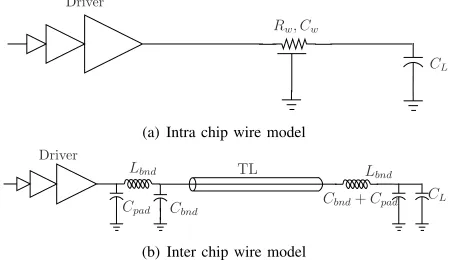
1) On-Chip Wire Delay: Typically global on-chip wires are
highly resistive, and the inductance is negligible , and hence signal transmission - obeys the diffusion equation. Hence they can be modeled as a distributed resistance-capacitance (RC) line. The delay over a RC dominated wire with capacitive load,CL, connected at the far-end constitutes the driver delay
and the distributed wire delay to which a first-order Elmore approximation is:
trc= 0.693{Rd(Cd+cwL+CL) +rwLCL}+0.377rwcwL2
Rw, Cw
CL
Driver
(a) Intra chip wire model
Lbnd
Lbnd
Cpad Cbnd Cbnd
+Cpad CL TL
Driver
[image:5.612.65.293.63.193.2](b) Inter chip wire model
Fig. 4. Delay models for Intra and Inter Chip Interconnections
Finally the propagation delay on the on-chip wire, as shown in Figure 4(a), is the sum of the cascaded buffer delay (tdrv)
and the Elmore delay of the RC wire:
tintra=tdrv+trc (21)
2) Off-Chip Wire Delay: Inter-chip wires on a typical
package substrate are characterized by low-loss dielectrics and by conductors with low resistivity and a large cross section, making losses due to shunt conductance negligible. Hence signal transmission exhibits transmission line behaviour. In a lossy transmission line, both RC and LC delays co-exist. For aLC dominated wires, the signal propagation delay is equal to its time-of-flight.
tLC =ttof =L
lwcw (22)
If a wire is a very resistive transmission line, the following empirical formula for adding time-of-flight (ttof) and
conven-tional RC delay (trc) was found in [29] to accurately predict
the total wire delay:
tRLC = (t1tof.6 +t1rc.6)
1
1.6 (23)
For the inter-chip communication link shown in Figure 4(b), the following expressions can be derived:
trc= 0.693
Z0(Cd+Cpad+Cbnd+ 0.5CL) +
Lbnd
Z0 +rwL(Cpad+Cbnd+CL)] + 0.4rwcwL2 (24)
Finally, the total delay for the inter-chip communication link is the summation of the cascaded driver delay (tdrv), the
RLC-wire delay (tRLC):
tinter=tdrv+tRLC (25)
IV. TRADEOFFANALYSIS FORSOC,SOPAND3D
IMPLEMENTATIONS
To make the comparison, we begin by selecting two mixed-signal systems. first system is a Wireless Sensor, which contain a 2Mb DRAM, and an ASIC and Microprocessor with gate count of 500k and 300k respectively. It also contains an Analog/RF block occupying an area of 2 mm2. Finally , it contains a MEMS sensor with an area of 1mm2. The
Notation Parameter Value
Do Defect Density perm2 250
S Shape Factor 0.6
Ndram DRAM Mask Layers 13
Nlogic Logic mask Layers 18
NRF CMOS RF Mask Layers 12
NM EM S MEMS Process Mask Layers 6
NCIS CMOS Image Sensor Process Mask Layers 10
Dwaf er Wafer Diameter 300mm
Clgc Process cost per mask layer (logic) 700 $
Cmixed Process cost per mask layer (mixed-signal) 1000 $
Cmcm MCM-D cost per unit area per layer 1000 $
Casmb Cost of assembly per pin 0.01
Csub Cost of substrate 300 $
C3Dvia Cost of making a through hole via in WLP 0.01 $
Crewrk Cost of Rework 3 $ $
CSOI Cost of SOI substrate 2000 $
Cwf r tst Wafer Test Cost per die 0.75 $
F Cwf r Wafer Test Coverage 80%
Cburnin Die Burn-In and test Cost 2 $
F Cdie Die Test coverage 99%
Cmod tst Module/Chip test cost 5 $
F Cmod Module/Chip test coverage 95%
YM CM sub Yield of MCM substrate production 0.98
Yasmb Yield of assembly 0.97
Y3Dsub Yield of Wafer Level 3D stacking 0.98
α, β, γ Area merging factors 2,1,1
Kp Rent’s Coeff. (ASIC, DRAM) 7, 1.4
Rent’s Coeff. (µP, module) 7, 1.4
ρ Rent’s Exp (ASIC, DRAM) 0.3, 0.12
Rent’s Exp (µP, module) 0.21, 0.63
Pw Contacted Metal Pitch 136nm
nw Number of interconnection layers (on-chip) 11
ew Utilization efficiency of interconnections 0.5
fg fanout of gates 2
Pp Peripheral in-line pad pitch 60µm
Ag Gate Area 1µm
Adramcell DRAM Cell Area[30], [2] 0.05µm
nw mcm Number of interconnection layers (MCM-D) 8
Pw mcm Interconnect pitch (MCM-D) 20µm
lbw Length of bondwire 1mm
Lbw Inductance of bondwire 2nH
Cbw Capacitance of bondwire 0.3pF
Rd Min. sized Buffer Output Resistance 20.8kΩ
Cg Min. sized Buffer Input Capacitance 0.14f F
Cd Min. sized Buffer Output Capacitance 0.22f F
Rv Resistance of through-hole via[31] 0.35Ω
Cv Capacitance of through-hole via[31] 5f F
Cpad Capacitance of the bond pad 2pF
tlayer Total Thickness of a Die 20µm
tglue Thickness of the glue layer in 3-D stack 2µm
tCu Thickness of Cu metalization layers per die 12µm
TABLE I
REPRESENTATIVEVALUES FOR A65nmTECHNOLOGY ANDNOTATIONS
FORMAJORPARAMETERS USED IN THE ANALYSIS. THESE VALUES VARY
WITH THE PROCESS TECHNOLOGY AND
second system is a 3G mobile terminal. We consider a similar architecture as the first one but with a larger memory of 128 M b DRAM, and a CMOS image sensor with a pixel size of1.75µm×1.75µm, and resolution of 8 M egapixel [32]. Further, in the analysis, we consider the ASIC and Microprocessor together as a single logic block, treating our target system as comprising only four megacells: analog/RF, logic, memory, and a MEMS or CMOS image sensor. For all the integration schemes, the underlying manufacturing process is a 65nm, 11-metal, CMOS process with a wafer diameter of 300 mm and a lower-level wire pitch of 136 nm. We
Parameter On-Chip Off-Chip
Physical
W(nm) 290 15
T(nm) 319 5
H(nm) 290 25
S(nm) 145 50
kILD 2.5 3.5
Electrical
Rw(Ω/mm) 237 0.02
Cw(f F/mm) 137 83
lw(nH/mm) 0.13 0.41
Z0(Ω) 31 70
TABLE II
ON-CHIP ANDOFF-CHIPWIREPARAMETERS[35]
also assume peripheral in-line pad arrangement and wire bond packaging. All the other key parameters are listed in Table I. The worst-case delay for 2-D systems is estimated diagonally from chip edge to chip edge, while it is estimated from one edge of the bottom chip to the opposite side edge of the top most chip for 3-D systems.
Based on the manufacturers data, the power density for the constituent sub-modules in our case studies can be es-timated. The power density for a DRAM is estimated to be 0.02W/mm2 [33], and for a logic block, 0.12W/mm2[34]. A CMOS Image sensor has an average power density of 0.016W/mm2. The power dissipation of the MEMS sen-sor is assumed to be 50mW, and that for the Analog/RF block,500mW. For the stacked arrangement, we assume that the logic block is close to the heat sink and other blocks are in the following order: DRAM, Analog/RF block, and MEMS/CMOS Image sensor.
A. Monolithic SoC
The integration of mixed signal systems in a single die is a merging of several technologies, such as logic, memory, analog/RF, and this results in increased process complexity and area. For example merging logic circuits with memory results in a lower circuit density and hence a larger circuit area, than their logic-only or memory-only counter parts. For example, in a UMC 0.18um technology a 6T-SRAM cell size is about 4 µm2 in a pure CMOS implementation, but is 5.6 µm2when merged. In this case the cell area increases by factor of 1.4 when merging processes [12]. If modules P, Q and R are merged into a single chip, the integrated areas composite systems comprising two and three modules respectively are shown in [12] to be:
AP∪Q = αAP +βAQ (32)
AP∪Q∪R = αAP +βAQ+γAR (33)
The total number of mask layers after merging is:
NP∪Q = NP +NQ−NP∩Q (34)
NP∪Q∪R = NP +NQ+NR−NP∩Q − NP∩R−NQ∩R
+ NP∩Q∩R (35)
The total cost for an SoC implementation is given in (27). Note that we assumed a MEMS-CMOS combined process for
SoC implementation of the first system, the wireless sensor node.
Multiplying the total power dissipation by the series com-bination of the substrate and package thermal resistances, we can estimate the average chip temperature.
B. 2D-SoP
In the 2D-SoP implementation, we assume that four chips (DRAM, RF, Logic and MEMS/Image Sensor) are assembled as a multi chip module (MCM). Hence, the cost of implement-ing the MCM includes the total cost for each chip includimplement-ing the testing, the assembly cost, the substrate cost, the rework cost, and finally the MCM test cost and packaging cost.
The SoP can provide some reworking capability whereas SoC and wafer-level 3-D integration do not. If one rework cycle is assumed for SoP, the yield in assembly is improved fromYato(2−Ya)Ya. Then the cost for SoP is given by (28)
and the overall yield as described in [36] is:
YSoP =Y(1− F c)
dram Y
(1−F c)
logic Y
(1−F c)
rf Y
(1−F c)
other Ya (36)
whereYotheris the yield of the MEMS sensor or CMOS image
sensor.
The overall temperature is found by estimating the effective chip thermal resistance from Ref f SoP =
n i=1
ti
kiAi and
then multiplying total power dissipation of all the chips by the series combination of thermal resistances Ref f SoP,
Rpkg(Package), andmRsubs(substrate).
C. 3D-SiP
A 3D-SiP implementation is similar to the SoP package integration, except that the SiP implementation integrate dies on top of each other vertically. The cost formula is the same, but the MCM substrate area is reduced, compared to the 2D-SoP implementation. The thermal profile is also found in a similar manner, using (19).
D. 3D-WLI
The yield of each 3-D implementation method is the cum-mulative yield over all the layers (m) and is given by:
Y3D = Y2D m−1
i=1
Y2DiYa (37)
whereY2Dis the fabrication yield of the 2D process, andYa
is the yield loss due to the 3-D assembly process. TheYm−1 a
term in the equation take into account the fact that integration ofm layers of chips requiresm−1 silicon growth or wafer bonding procedures. In the case of D2W stacking, die yield after the KGD testing should be considered. Hence the overall yield for implementing our target system in W2W and 3D-D2W methods as described in [36], [37] are as follows:
Y3D w2w = YdramYlogicYrfYotherYa3 (38)
Y3D22w = Y(1− F c)
dram Y
(1−F c)
logic Y
(1−F c)
rf Y
(1−F c)
other Ya3(39)
CSoC=
Cwaf er
YSoCNdie+
Cwaf er test
1 P Fw +
Cburn in
1 P Fb +
Cpkg (27)
CSoP =
m
i=1
Ckgdi+
Csubstrate
Ys +Cassembly+Crework
Ya +
Ctest
1 P FSoP +
Cpkg (28)
C3D SiP =
m
i=1
Ckgdi+
Csubstrate
Ys +Cassembly+Crework
Ya +
Ctest
1
P F3D SiP +
Cpkg (29)
C3D W2W =
m
i=1
Cdiei+Cbonding
Ya3D W2W +
Ctest
1 P FW2W +
Cpkg (30)
C3D D2W =
m
i=1
Ckgdi+Cbonding
Ya 3D D2W +
Ctest
1 P FD2W +
Cpkg (31)
Case Wireless Sensor Node 3G Mobile Terminal
Parameter Single Chip 2D-SoP 3D-SiP 3D-W2W 3D-D2W Single Chip 2D-SoP 3D-SiP 3D-W2W 3D-D2W
Normalized Area 1.00 3.92 0.78 0.71 0.71 1.00 1.94 0.75 0.71 0.71
Yieldoverall 0.95 0.98 0.98 0.92 0.94 0.56 0.98 0.98 0.71 0.94
Normalized Cost 1.00 4.11 4.04 1.14 2.96 1.00 0.40 0.40 0.38 0.33
Delay (ps) 127.37 176.36 148.33 83.9 83.9 317.88 205.37 168.34 259.63 259.63
∆T(oC) 39.16 12.39 52.8 312.74 312.74 26.38 14.67 36.9 73.96 73.96
TABLE III
RESULTS OFCOSTPERFORMANCE ANALYSIS FORCASE-STUDIES. NOTE THAT∆T=Ttop layer−Tambient.
there is no possibility of reworking. In a W2W integration methodology all dies must be as same as in size in order to alleviate manufacturing difficulties, especially the precise alignment of wafers to make the vertical interconnections, and dicing, whereas for D2W integration the dies can be different in size. Moreover, though there is an area penalty due to the vertical interconnections, it is assumed that the area of the state-of-the art THV is on the order of a fewµm2[31]. Again thermal profile is calculated using (19).
V. DISCUSSION
Results for our case studies are shown in Table III. It is quite obvious that 3-D integration provides very compact designs compared to its 2-D planar counterpart. Except for the 3D-SiP method, 3D-WLI has lower interconnect delays over the 2-D implementations. 32-D-SiP and 22-D-SoP implementations are more or less equal in implementation cost, but 3D-SiP has a lower interconnect delay. Where the wireless sensor node is concerned, the SoC solution is the better choice, while wafer-level 3D integration provides lower area and higher performance. A SoC solution is the best option for such low memory applications because it is less expensive. However,
though quite expensive, for high performance systems, 3D-WLI is the best choice.
The scenario is different when it comes to a mobile terminal. In this case, the overall chip area is 4.25 times larger than that of the wireless sensor node. 3D-WLI technologies outperform SiP implementation technologies, due to the very long RC wires. Also, single chip solution has a very low yield. All the other implementations methods show a lower cost than the single chip implementation. 3D-SiP seems to be the best design choice for low-cost, and high performance in this case. The case studies show that when the system size becomes very small the thermal resistance becomes high the temper-ature rise in the top-most chip is unbearable. Hence, extra cooling solutions such as thermal-vias occupying some area, or very thin layers have to be used in the system implementation.
VI. CONCLUSION
In this paper, we developed a detailed yield and quantitative cost models, and a quantitative performance metric for 3-D in-tegration. Further, we derived simple yet useful thermal models for 2-D and 3-D integrated circuits. The overall methodology is suitable for early analysis in system explorations for future nanoscale electronic systems. Through some example
porary mixed signal systems we demonstrate the methodology outlined for different implementations and conclude that the implementation strategy must be carefully selected depending on the circuit complexity, as else the move to 3-D may have a detrimental effect. Design choice early in the design cycle will have a significant impact throughout the design and production lifecycles , and the models and methodology presented in this article can be an important aid in this choice.
REFERENCES
[1] F. Catthoor, N. D. Dutt, and C. E. Kozyrakis, “How to solve the current memory access and data transfer bottlenecks: at the processor architecture or at the compiler level,” in DATE ’00: Proceedings of the
conference on Design, automation and test in Europe. New York, NY,
USA: ACM Press, 2000, pp. 426–435.
[2] The International Technology Roadmap for Semiconductors(ITRS), 2005. [Online]. Available: http://www.itrs.net
[3] E. Beyne, “3d interconnection and packaging: impending reality or still a dream?” in Solid-State Circuits Conference, 2004. Digest of Technical
Papers. ISSCC. 2004 IEEE International, 2004, pp. 138–139 Vol.1.
[4] M. Bamal, S. List, M. Stucchi, A. Verhulst, M. Van Hove, R. Cartuyvels, G. Beyer, and K. Maex, “Performance comparison of interconnect technology and architecture options for deep submicron technology nodes,” in Interconnect Technology Conference, 2006 International, 2006, pp. 202–204.
[5] S. Kim, C. Liu, L. Xue, and S. Tiwari, “Crosstalk reduction in mixed-signal 3-d integrated circuits with interdevice layer ground planes,”
Electron Devices, IEEE Transactions on, vol. 52, no. 7, pp. 1459–1467,
2005.
[6] K. Banerjee, S. J. Souri, P. Kapur, and K. C. Saraswat, “3-d ics: A novel chip design for improving deep-submicrometer interconnect performance and systems-on-chip integration,” Proceedings of the IEEE, vol. 89, no. 5, pp. 602–633, May 2001.
[7] B. Goplen and S. Sapatnekar, “Placement of thermal vias in 3-d ics using various thermal objectives,” Computer-Aided Design of Integrated
Circuits and Systems, IEEE Transactions on, vol. 25, no. 4, pp. 692–709,
2006.
[8] Z. Li, X. Hong, Q. Zhou, S. Zeng, J. Bian, W. Yu, H. H. Yang, V. Pitchu-mani, and C.-K. Cheng, “Efficient thermal via planning approach and its application in 3-d floorplanning,” Computer-Aided Design of Integrated
Circuits and Systems, IEEE Transactions on, vol. 26, no. 4, pp. 645–658,
2007.
[9] J. Koo, S. Im, L. Jiang, and K. Goodson, “Integrated microchannel cooling for three-dimensional circuit architectures,” ASME Journal of
Heat Transfer, vol. 127, pp. 49–58, 2005.
[10] B. Dang, M. Bakir, and J. Meindl, “Integrated thermal-fluidic i/o interconnects for an on-chip microchannel heat sink,” Electron Device
Letters, IEEE, vol. 27, pp. 117–119, February 2006.
[11] G. Luca, B. Agrawal, N. Srivastava, S.-C. Lin, T. Sherwood, and K. Banerjee, “A thermally-aware performance analysis of vertically integrated (3-d) processor-memory hierarchy,” in DAC ’06: Proceedings
of the 43rd annual conference on Design automation. New York, NY, USA: ACM Press, 2006, pp. 991–996.
[12] M. Shen, L.-R. Zheng, and H. Tenhunen, “Cost and performance analysis for mixed-signal system implementation: System-on-chip or system-on-package,” Electronics Packaging Manufacturing, IEEE Journal of, vol. 25, no. 4, pp. 262–272, October 2002.
[13] C. Liu, J.-H. Chen, R. Manohar, and S. Tiwari, “Mapping system-on-chip designs from 2-d to 3-d ics,” in Circuits and Systems, 2005. ISCAS
2005. IEEE International Symposium on, 2005, pp. 2939–2942 Vol. 3.
[14] P. Mercier, S. Singh, K. Iniewski, B. Moore, and P. O’Shea, “Yield and cost modeling for 3d chip stack technologies,” in Conference 2006,
IEEE Custom Integrated Circuits, September 2006, pp. 357–360.
[15] R. K. Ulrich and W. D. Brown, Eds., Advanced Electronic Packaging,
2nd ed., ser. IEEE Press Series on Microelectronic Systems.
Wiley-Interscience, September 2005.
[16] M. Dreiza, A. Yoshida, J. Micksch, and L. Smith, “Stacked package-on-package design guidelines,” ChipScale Review, Amkor Technology Inc., July 2005.
[17] T. Fukushima, Y. Yamada, H. Kikuchi, and M. Koyanagi, “New three-dimensional integration technology using chip-to-wafer bonding to achieve ultimate super-chip integration,” Japanese Journal of Applied
Physics, vol. 45, no. 4B, pp. 3030–3035, 2006.
[18] E. Culurciello and A. G. Andreou, “Capacitive inter-chip data and power transfer for 3-d vlsi,” Circuits and Systems II: Express Briefs, IEEE
Transactions on [see also Circuits and Systems II: Analog and Digital Signal Processing, IEEE Transactions on], vol. 53, no. 12, pp. 1348–
1352, 2006.
[19] A. Fazzi, L. Magagni, M. Mirandola, R. Canegallo, S. Schmitz, and R. Guerrieri, “A 0.14mw/gbps high-density capacitive interface for 3d system integration,” in Custom Integrated Circuits Conference, 2005.
Proceedings of the IEEE 2005, 2005, pp. 101–104.
[20] J. Xu, J. Wilson, S. Mick, L. Luo, and P. Franzon, “2.8 gb/s inductively coupled interconnect for 3d ics,” in VLSI Circuits, 2005. Digest of
Technical Papers. 2005 Symposium on, 2005, pp. 352–355.
[21] A. Iwata, M. Sasaki, T. Kikkawa, S. Kameda, H. Ando, K. Kimoto, D. Arizono, and H. Sunami, “A 3d integration scheme utilizing wireless interconnections for implementing hyper brains,” in Solid-State Circuits
Conference, 2005. Digest of Technical Papers. ISSCC. 2005 IEEE International, 2005, pp. 262–597 Vol. 1.
[22] H. B. Backoglu, Circuits, Interconnections and Packaging for VLSI. Addison-Wesley, 1990.
[23] W. Donath, “Placement and average interconnection lengths of computer logic,” Circuits and Systems, IEEE Transactions on, vol. 26, no. 4, pp. 272–277, 1979.
[24] P. Zarkesh-Ha, J. Davis, and J. Meindl, “Prediction of net-length distribution for global interconnects in a heterogeneous system-on-a-chip,” Very Large Scale Integration (VLSI) Systems, IEEE Transactions
on, vol. 8, no. 6, pp. 649–659, 2000.
[25] P. A. Sandborn and H. Moreno, Conceptual Design of Multichip Modules
and Systems. Kluwer Academic Publishers, 1994.
[26] A. George, J. Krusius, and R. Granitz, “Packaging alternatives to large silicon chips: tiled silicon on mcm and pwb substrates,” Components,
Packaging, and Manufacturing Technology, Part B: Advanced Pack-aging, IEEE Transactions on [see also Components, Hybrids, and Manufacturing Technology, IEEE Transactions on], vol. 19, no. 4, pp.
699–708, 1996.
[27] D. Ragan, P. Sandborn, and P. Stoaks, “A detailed cost model for concurrent use with hardware/software co-design,” in Design Automation
Conference, 2002. Proceedings of IEEE/ACM, 2002, pp. 269–274.
[28] S. Im and K. Banerjee, “Full chip thermal analysis of planar (2-d) and vertically integrated (3-d) high performance ics,” in Electron Devices
Meeting, 2000. IEDM Technical Digest. International, 2000, pp. 727–
730.
[29] G. Sai-Halasz, “Performance trends in high-end processors,”
Proceed-ings of the IEEE, vol. 83, no. 1, pp. 20–36, 1995.
[30] R. Waiser, Ed., Nanoelectronics and Information Technology: Advanced
Electronic Materials and Novel Devices. Wiley-VCH, September 2004.
[31] R. Patti, “Three-dimensional integrated circuits and the future of system-on-chip designs,” Proceedings of the IEEE, vol. 94, no. 6, pp. 1214– 1224, 2006.
[32] Micron CMOS Image Sensor Part Catalog, March 2007. [Online]. Available: http://www.micron.com
[33] Micron 128MB SDRAM Part Catalog, 2007. [Online]. Available: http://www.micron.com
[34] ARM Cortex-A8 Processor Product Brief, March 2007. [Online]. Available: http://www.arm.com
[35] L.-R. Zheng, D. Pamunuwa, and H. Tenhunen, “Accurate a priori signal integrity estimation using a multilevel dynamic interconnect model for deep submicron vlsi design,” in Solid-State Circuits Conference, 2000.
ESSCIRC ’00. Proceedings of the 26th European, 2000, pp. 352–355.
[36] Y. Deng and W. P. Maly, “2.5-dimensional vlsi system integration,” very
large scale integration (VLSI) systems , IEEE Transactions of, vol. 13,
no. 6, pp. 668–677, June 2005.
[37] E. Beyne, “The rise of the 3rd dimension for system intergration,” in